7-1847
August 1997
HI7188
8-Channel, 16-Bit, High Precision,
Sigma-Delta A/D Sub-System
Features
· Fully Differential 8-Channel Multiplexer and Reference
· Automatic Channel Switching with Zero Latency
· 240 Conversions Per Second Per Channel
· 16-Bit Resolution with No Missing Codes
· 0.0015% Integral Non-Linearity
· Fully Software Configurable
- -120dB Rejection of 60/50Hz Line Noise
- Channel Conversion Order and Number of Active
Channels
- True Bipolar or Unipolar Input Range Per Channel
- PGIA Gain Per Channel
- 2-Wire or 3-Wire Interface
· Chopper Stabilized PGIA with Gains of 1 to 8
· Serial Data I/O Interface, SPI Compatible
· 3 Point System Calibration
· Low Power Dissipation of 30mW (Typ)
Applications
· Multi-Channel Industrial Process Controls
· Weight Scales
· Medical Patient Monitoring
· Laboratory Instrumentation
· Gas Monitoring System
· Reference Literature
- AN9504 "A Brief Introduction to Sigma Delta
Conversion"
- TB329 "Intersil Sigma-Delta Calibration Tech-
niques"
- AN9518 "Using the HI7188 Evaluation Kit"
- AN9610 "Interfacing the HI7188 to a Microcontroller"
- AN9538 "Using the HI7188 Serial Interface"
Description
The HI7188 is an easy-to-use 8-Channel sigma-delta pro-
grammable A/D subsystem ideal for low frequency physical
and electrical measurements in scientific, medical, and
industrial applications. The subsystem has complete on-chip
capabilities to support moving the intelligence from the sys-
tem controller and towards the sensors. This gives the
designer faster and more flexible configurability without the
traditional drawbacks of low throughput per channel, higher
power or cost per channel. Extreme design complexity and
excessive software overhead is eliminated.
The HI7188 contains a fully differential 8 channel multiplexer,
Programmable Gain Instrumentation Amplifier (PGIA), 4th
order sigma-delta ADC, integrating filter, line noise rejection
filters, calibration and data RAMs, clock oscillator, and a
microsequencer. Communication with the HI7188 is per-
formed via the serial I/O port, and is compatible with most
synchronous transfer formats, including both the Motor-
ola/Intersil 6805/11 series SPI, QSPI and Intel 8051 series
SSR protocols.
The powerful on-board microsequencer provides automatic
conversions on the multiplexed input channels (up to 8) by
controlling all channel switching, filtering and calibration. The
microsequencer supports on-the-fly multiplexer reconfigura-
tion, forty to fifty times faster throughput than the competition
and zero step response delay during internal or external
multiplexer channel changes. A simple set of commands
gives the user control over calibration, PGIA gain, and bipo-
lar/unipolar modes on a per channel basis. Number of chan-
nels to convert, data coding, line noise rejection, etc. is
programmed at the chip level. The calibration RAMs allow
the user to read and write system calibration data while the
data RAMs provide a read support of the conversion results
for each channel.
This design is effectively eight 16-bit (for 96dB noise-free
dynamic range) Sigma-Delta A/D converters combined with
a microsequencer and an eight-channel multiplexer in a sin-
gle package. The HI7188 provides 120dB line-noise rejec-
tion at 240 samples/second/channel (in 60Hz line-rejection
mode) and 200 samples/second/channel (in 50Hz line-rejec-
tion mode) base output data rates. By reusing multiplexer
channels for the same input, throughput can increase by
integer increments of the base output data rate up to
1920Hz.
Ordering Information
PART
NUMBER
TEMP.
RANGE (
o
C)
PACKAGE
PKG. NO.
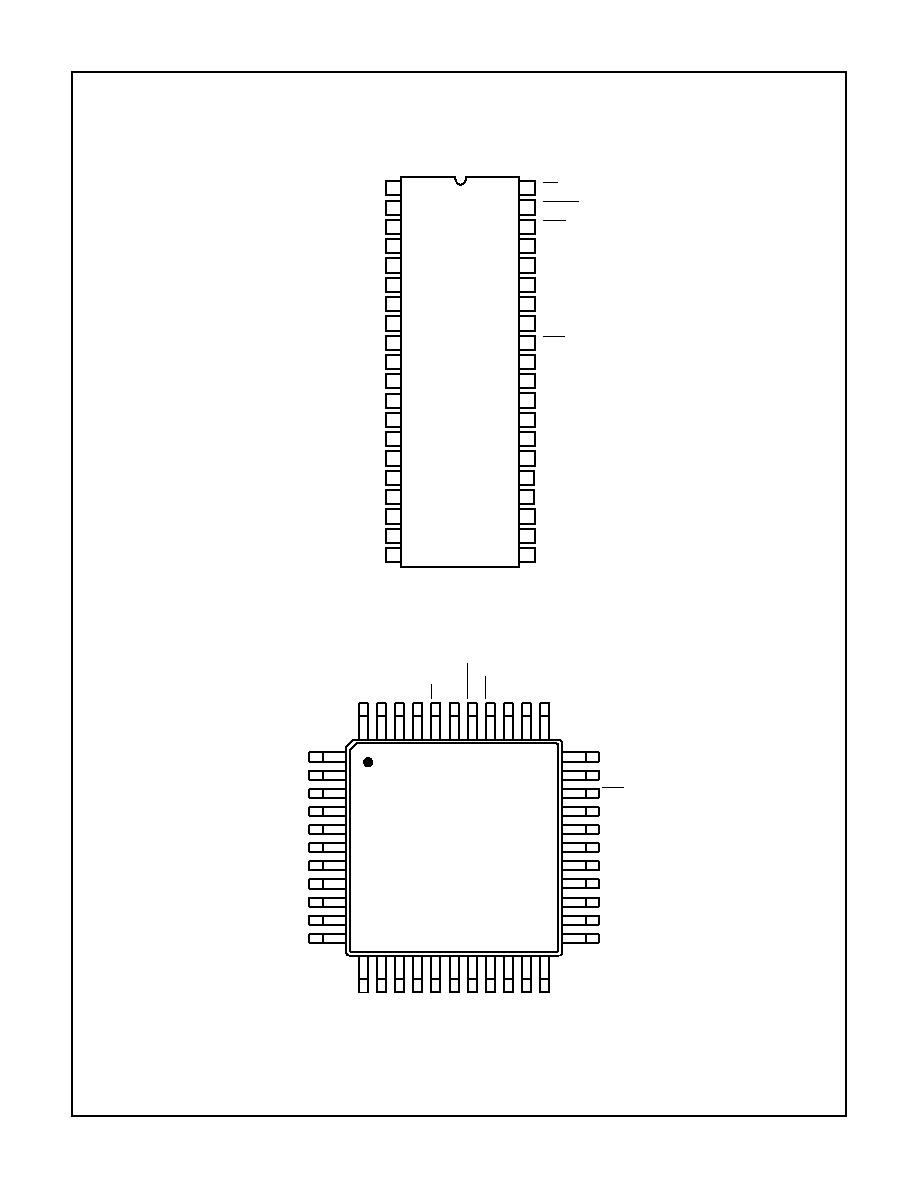
HI7188IP
-40 to 85
40 Ld PDIP
E40.6
HI7188IN
-40 to 85
44 Ld MQFP
Q44.10x10
HI7188EVAL
25
Evaluation Kit
File Number
4016.4
CAUTION: These devices are sensitive to electrostatic discharge; follow proper IC Handling Procedures.
http://www.intersil.com or 407-727-9207
|
Copyright
©
Intersil Corporation 1999
7-1851
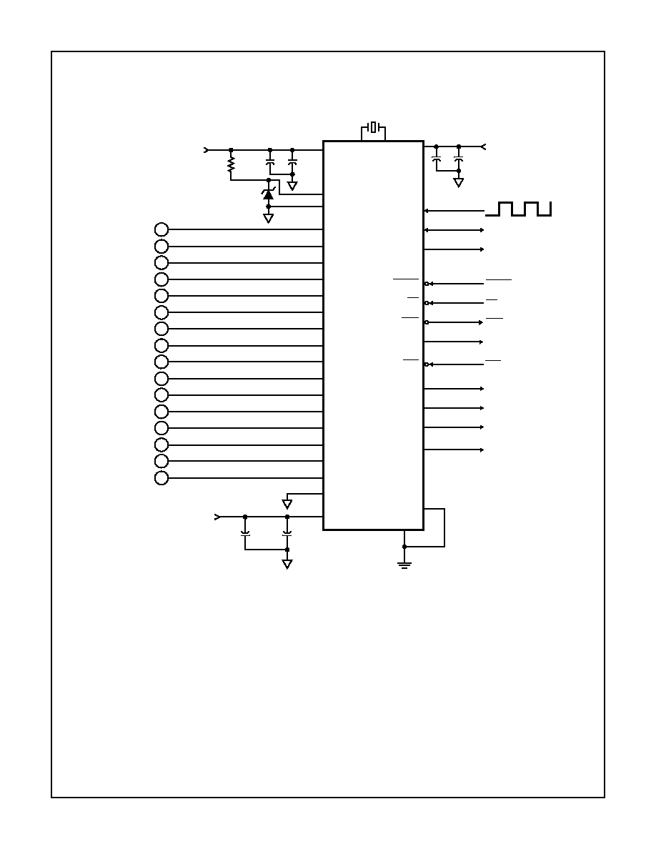
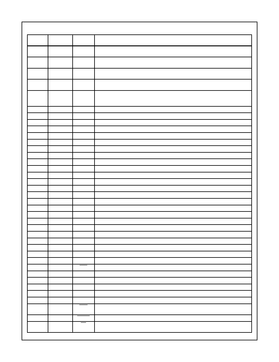
Pin Descriptions
40 LEAD
PDIP
44 LEAD
MQFP
PIN NAME
PIN DESCRIPTION
1
41
MODE
Mode input. Used to select between Synchronous Self Clocking (MODE = 1) or Synchronous Ex-
ternal Clocking (MODE = 0) for the Serial Port.
2
42
SCLK
Serial interface clock. Synchronizes serial data transfers. Data is input on the rising edge and out-
put on the falling edge.
3
43
SDO
Serial Data Out. Serial data is read from this line when using a 3-wire serial protocol such as the
Motorola Serial Peripheral Interface.
4
44
SDIO
Serial Data IN or OUT. This line is bidirectional programmable and interfaces directly to the Intel
Standard Serial Interface using a 2-wire serial protocol.
5
1
OSC
1
Oscillator clock input for the device. A crystal connected between OSC
1
and OSC
2
will provide a
clock to the device, or an external oscillator can drive OSC
1
. The oscillator frequency should be
3.6864MHz to maintain Line Noise Rejection.
6
2
OSC
2
Used to connect a crystal source between OSC
1
and OSC
2
. Leave open otherwise.
7
3, 30
DV
DD
Positive Digital supply (+5V).
8, 31
4, 29, 39
DGND
Digital supply ground.
9, 30
5, 6, 27, 28
AV
SS
Negative analog power supply (-5V).
10
7
V
INL1
Analog input low for Channel 1.
11
8
V
INH1
Analog input high for Channel 1.
12
9
V
INL2
Analog input low for Channel 2.
13
10
V
INH2
Analog input high for Channel 2.
14
11
V
INL3
Analog input low for Channel 3.
15
12
V
INH3
Analog input high for Channel 3.
16
13
V
INL4
Analog input low for Channel 4.
17
14
V
INH4
Analog input high for Channel 4.
18
15
V
INL5
Analog input low for Channel 5.
19
16
V
INH5
Analog input high for Channel 5.
20
17
V
INL6
Analog input low for Channel 6.
21
18
V
INH6
Analog input high for Channel 6.
22
19
V
INL7
Analog input low for Channel 7.
23
20
V
INH7
Analog input high for Channel 7.
24
21
V
INL8
Analog input low for Channel 8.
25
22
V
INH8
Analog input high for Channel 8.
26
23
V
CM
Common mode voltage. Must be tied to the mid point of AV
DD
and AV
SS
.
27
24
V
RLO
External reference input. Should be negative referenced to V
RHI
.
28
25
V
RHI
External reference input. Should be positive referenced to V
RLO
.
29
26
AV
DD
Positive analog power supply (+5V).
32
31
RST
Active low Reset pin. Used to initialize modulator, filter, RAMs, registers and state machines.
33
32
CA
Calibration active output. Indicates that at least one active channel is in a calibration mode.
34
33
MXC
Multiplexer control output. Indicates that the conversion for the active channel is complete.
35
34
A
0
Logical channel count output (LSB).
36
35
A
1
Logical channel count output.
37
36
A
2
Logical channel count output (MSB).
38
37
EOS
End of scan output. Signals the end of a channel scan (all active channels have been converted)
and data is available to be read. Remains low until data RAM is read.
39
38
RSTI/O
I/O reset (active low) input. Resets serial interface state machine only.
40
40
CS
Active low chip select pin. Used to select a serial data transfer cycle. When high the SDO and
SDIO pins are three-state.
HI7188