70
CAUTION: These devices are sensitive to electrostatic discharge; follow proper IC Handling Procedures.
1-888-INTERSIL or 321-724-7143
|
Copyright
®
Intersil Corporation 1999
HI5746
10-Bit, 40 MSPS A/D Converter
The HI5746 is a monolithic, 10-bit, analog-to-digital
converter fabricated in a CMOS process. It is designed for
high speed applications where wide bandwidth and low
power consumption are essential. Its 40 MSPS speed is
made possible by a fully differential pipelined architecture
with an internal sample and hold.
The HI5746 has excellent dynamic performance while
consuming only 225mW power at 40 MSPS. Data output
latches are provided which present valid data to the output
bus with a latency of 7 clock cycles. It is pin-for-pin
functionally compatible with the HI5702 and the HI5703.
For internal voltage reference, please refer to the HI5767
data sheet.
Features
À Sampling Rate . . . . . . . . . . . . . . . . . . . . . . . . . . 40 MSPS
À 8.8 Bits at f
IN
= 10MHz
À Low Power at 40 MSPS . . . . . . . . . . . . . . . . . . . . 225mW
À Wide Full Power Input Bandwidth . . . . . . . . . . . . 250MHz
À On-Chip Sample and Hold
À Fully Differential or Single-Ended Analog Input
À Single Supply Voltage. . . . . . . . . . . . . . . . . . . . . . . . . +5V
À TTL/CMOS Compatible Digital Inputs
À CMOS Compatible Digital Outputs . . . . . . . . . . . . 3.0/5.0V
À Offset Binary or Two's Complement Output Format
Applications
À Professional Video Digitizing
À Medical Imaging
À Digital Communication Systems
À High Speed Data Acquisition
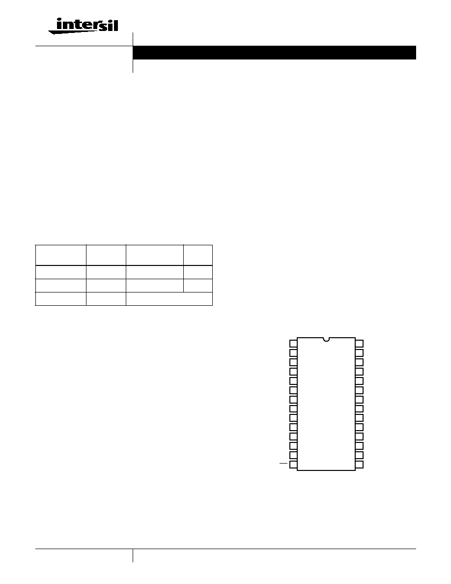
Pinout
HI5746
(SOIC, SSOP)
TOP VIEW
Ordering Information
PART
NUMBER
TEMP.
RANGE (
o
C)
PACKAGE
PKG.
NO.
HI5746KCB
0 to 70
28 Ld SOIC (W)
M28.3
HI5746KCA
0 to 70
28 Ld SSOP
M28.15
HI5746EVAL1
25
Evaluation Board
28
27
26
25
24
23
22
21
20
19
18
17
16
15
DV
CC1
DGND1
DV
CC1
DGND1
AV
CC
AGND
V
REF
+
V
REF
-
V
IN
+
V
IN
-
V
DC
AGND
AV
CC
OE
1
2
3
4
5
6
7
8
9
10
11
12
13
14
D0
D2
D3
D4
DV
CC2
DGND2
D6
D7
D8
D9
DFS
D1
CLK
D5
Data Sheet
February 1999
File Number
4129.4

71
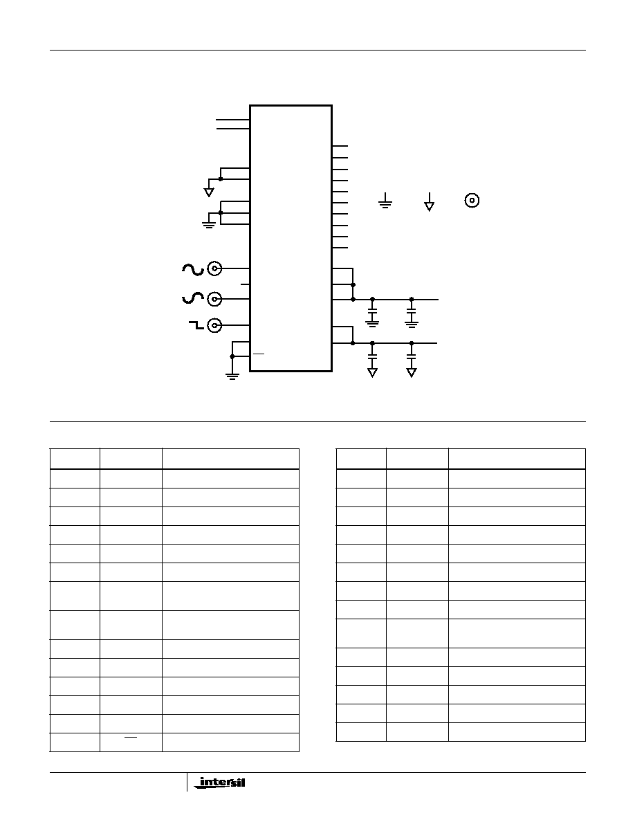
Functional Block Diagram
DV
CC2
DGND2
OE
+
-
STAGE 1
STAGE 8
CLOCK
BIAS
V
DC
V
IN
-
V
IN
+
D0 (LSB)
D1
D2
D3
D4
D5
D6
D7
D8
D9 (MSB)
CLK
DFS
AV
CC
AGND
DV
CC1
DGND1
V
REF
+
V
REF
- (OPTIONAL)
STAGE 9
X2
S/H
2-BIT
FLASH
2-BIT
DAC
+
-
X2
2-BIT
FLASH
2-BIT
DAC
2-BIT
FLASH
DIGITAL DELAY
AND
DIGITAL ERROR
CORRECTION
HI5746
72
Typical Application Schematic
Pin Descriptions
HI5746
ARE PLACED AS CLOSE
10
Á
F AND 0.1
Á
F CAPS
D9
D8
D7
D6
D5
D4
D3
D2
D1
D0
BNC
CLOCK
V
IN
+
10
Á
F
0.1
Á
F
10
Á
F
+
+
2.5V
2.0V
V
IN
-
DGND
AGND
V
REF
- (8)
V
REF
+ (7)
V
IN
- (10)
CLK (22)
DFS (15)
DGND1 (4)
DGND2 (21)
DGND1 (2)
AGND (6)
AGND (12)
V
IN
+ (9)
(1) DV
CC1
V
DC
(11)
(LSB) (28) D0
(27) D1
(26) D2
(25) D3
(24) D4
(20) D5
(19) D6
(18) D7
(17) D8
(MSB) (16) D9
(5) AV
CC
(13) AV
CC
(23) DV
CC2
(3) DV
CC1
TO PART AS POSSIBLE
OE (14)
0.1
Á
F
+5V
+5V
(OPTIONAL)
PIN NO.
NAME
DESCRIPTION
1
DV
CC1
Digital Supply (+5.0V).
2
DGND1
Digital Ground.
3
DV
CC1
Digital Supply (+5.0V).
4
DGND1
Digital Ground.
5
AV
CC
Analog Supply (+5.0V).
6
AGND
Analog Ground.
7
V
REF
+
+2.5V Positive Reference Voltage
Input.
8
V
REF
-
+2.0V Negative Reference Voltage
Input (Optional).
9
V
IN
+
Positive Analog Input.
10
V
IN
-
Negative Analog Input.
11
V
DC
DC Bias Voltage Output.
12
AGND
Analog Ground.
13
AV
CC
Analog Supply (+5.0V).
14
OE
Digital Output Enable Control Input.
15
DFS
Data Format Select Input.
16
D9
Data Bit 9 Output (MSB).
17
D8
Data Bit 8 Output.
18
D7
Data Bit 7 Output.
19
D6
Data Bit 6 Output.
20
D5
Data Bit 5 Output.
21
DGND2
Digital Ground.
22
CLK
Sample Clock Input.
23
DV
CC2
Digital Output Supply
(+3.0V or +5.0V).
24
D4
Data Bit 4 Output.
25
D3
Data Bit 3 Output.
26
D2
Data Bit 2 Output.
27
D1
Data Bit 1 Output.
28
D0
Data Bit 0 Output (LSB).
PIN NO.
NAME
DESCRIPTION
HI5746

73
Absolute Maximum Ratings
T
A
= 25
o
C
Thermal Information
Supply Voltage, AV
CC
or DV
CC
to AGND or DGND . . . . . . . . . . .6V
DGND to AGND . . . . . . . . . . . . . . . . . . . . . . . . . . . . . . . . . . . . . . . . 0.3V
Digital I/O Pins . . . . . . . . . . . . . . . . . . . . . . . . . . . . . DGND to DV
CC
Analog I/O Pins . . . . . . . . . . . . . . . . . . . . . . . . . . . . AGND to AV
CC
Operating Conditions
Temperature Range
HI5746KCB (Typ) . . . . . . . . . . . . . . . . . . . . . . . . . . . . 0
o
C to 70
o
C
Thermal Resistance (Typical, Note 1)
JA
(
o
C/W)
SOIC Package . . . . . . . . . . . . . . . . . . . . . . . . . . . . .
70
SSOP Package . . . . . . . . . . . . . . . . . . . . . . . . . . . .
100
Maximum Junction Temperature . . . . . . . . . . . . . . . . . . . . . . .150
o
C
Maximum Storage Temperature Range . . . . . . . . . .
-
65
o
C to 150
o
C
Maximum Lead Temperature (Soldering 10s) . . . . . . . . . . . . .300
o
C
(SOIC, SSOP - Lead Tips Only)
CAUTION: Stresses above those listed in "Absolute Maximum Ratings" may cause permanent damage to the device. This is a stress only rating and operation of the
device at these or any other conditions above those indicated in the operational sections of this specification is not implied.
NOTE:
1.
JA
is measured with the component mounted on an evaluation PC board in free air.
Electrical Specifications
AV
CC
= DV
CC1
= 5.0V; DV
CC2
= 3.0V, V
REF
+ = 2.5V; V
REF
- = 2.0V; f
S
= 40 MSPS at 50% Duty Cycle;
C
L
= 10pF; T
A
= 25
o
C; Differential Analog Input; Typical Values are Test Results at 25
o
C,
Unless Otherwise Specified
PARAMETER
TEST CONDITIONS
MIN
TYP
MAX
UNITS
ACCURACY
Resolution
10
-
-
Bits
Integral Linearity Error, INL
f
IN
= DC
-
▒
1.0
▒
2.0
LSB
Differential Linearity Error, DNL
(Guaranteed No Missing Codes)
f
IN
= DC
-
▒
0.5
▒
1.0
LSB
Offset Error, V
OS
f
IN
= DC
-40
12
40
LSB
Full Scale Error, FSE
f
IN
= DC
-
4
-
LSB
DYNAMIC CHARACTERISTICS
Minimum Conversion Rate
No Missing Codes
-
0.5
1
MSPS
Maximum Conversion Rate
No Missing Codes
40
-
-
MSPS
Effective Number of Bits, ENOB
f
IN
= 10MHz
8.55
8.8
-
Bits
Signal to Noise and Distortion Ratio, SINAD
f
IN
= 10MHz
53.2
54.9
-
dB
Signal to Noise Ratio, SNR
f
IN
= 10MHz
53.2
55.4
-
dB
Total Harmonic Distortion, THD
f
IN
= 10MHz
-
-64.6
-
dBc
2nd Harmonic Distortion
f
IN
= 10MHz
-
-67.8
-
dBc
3rd Harmonic Distortion
f
IN
= 10MHz
-
-68.3
-
dBc
Spurious Free Dynamic Range, SFDR
f
IN
= 10MHz
-
67.8
-
dBc
Intermodulation Distortion, IMD
f
1
= 1MHz, f
2
= 1.02MHz
-
64
-
dBc
Differential Gain Error
f
S
= 17.72 MSPS, 6 Step, Mod Ramp
-
0.8
-
%
Differential Phase Error
f
S
= 17.72 MSPS, 6 Step, Mod Ramp
-
0.1
-
Degree
Transient Response
(Note 2)
-
1
-
Cycle
Over-Voltage Recovery
0.2V Overdrive (Note 2)
-
1
-
Cycle
RMS Signal
RMS Noise + Distortion
--------------------------------------------------------------
=
RMS Signal
RMS Noise
-------------------------------
=
HI5746
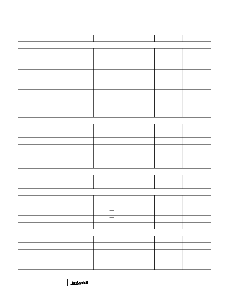
74
ANALOG INPUT
Maximum Peak-to-Peak Differential Analog Input
Range (V
IN
+ - V
IN
-)
-
▒
0.5
-
V
Maximum Peak-to-Peak Single-Ended
Analog Input Range
-
1.0
-
V
Analog Input Resistance, R
IN
(Note 3)
-
1
-
M
Analog Input Capacitance, C
IN
-
10
-
pF
Analog Input Bias Current, I
B
+ or I
B
-
(Note 3)
-10
-
+10
Á
A
Differential Analog Input Bias Current
I
BDIFF
= (I
B
+ - I
B
-)
(Note 3)
-
▒
0.5
-
Á
A
Full Power Input Bandwidth, FPBW
-
250
-
MHz
Analog Input Common Mode Voltage Range
(V
IN
+ + V
IN
-)/2
Differential Mode (Note 2)
0.25
-
4.75
V
REFERENCE INPUT
Total Reference Resistance, R
L
V
REF
+ to AGND
-
2.5K
-
Positive Reference Current, I
REF
+
-
1.07
-
mA
Negative Reference Current, I
REF
-
-
21
-
Á
A
Positive Reference Voltage Input, V
REF
+
(Note 2)
-
2.5
-
V
Negative Reference Voltage Input, V
REF
-
(Note 2)
-
2.0
-
V
Reference Common Mode Voltage
(V
REF
+ + V
REF
-)/2
(Note 2)
-
2.25
-
V
DC BIAS VOLTAGE
DC Bias Voltage Output, V
DC
-
3.2
-
V
Maximum Output Current
-
-
0.4
mA
DIGITAL INPUTS
Input Logic High Voltage, V
IH
CLK, DFS, OE
2.0
-
-
V
Input Logic Low Voltage, V
IL
CLK, DFS, OE
-
-
0.8
V
Input Logic High Current, I
IH
CLK, DFS, OE, V
IH
= 5V
-10.0
-
+10.0
Á
A
Input Logic Low Current, I
IL
CLK, DFS, OE, V
IL
= 0V
-10.0
-
+10.0
Á
A
Input Capacitance, C
IN
-
7
-
pF
DIGITAL OUTPUTS
Output Logic High Voltage, V
OH
I
OH
= 100
Á
A; DV
CC2
= 5V
4.0
-
-
V
Output Logic Low Voltage, V
OL
I
OL
= 100
Á
A; DV
CC2
= 5V
-
-
0.5
V
Output Three-State Leakage Current, I
OZ
V
O
= 0/5V; DV
CC2
= 5V
-
▒
1
▒
10
Á
A
Output Logic High Voltage, V
OH
I
OH
= 100
Á
A; DV
CC2
= 3V
2.4
-
-
V
Output Logic Low Voltage, V
OL
I
OL
= 100
Á
A; DV
CC2
= 3V
-
-
0.5
V
Electrical Specifications
AV
CC
= DV
CC1
= 5.0V; DV
CC2
= 3.0V, V
REF
+ = 2.5V; V
REF
- = 2.0V; f
S
= 40 MSPS at 50% Duty Cycle;
C
L
= 10pF; T
A
= 25
o
C; Differential Analog Input; Typical Values are Test Results at 25
o
C,
Unless Otherwise Specified (Continued)
PARAMETER
TEST CONDITIONS
MIN
TYP
MAX
UNITS
HI5746