
TM
1
HI3300
3V 10-Bit, 20MSPS A/D Converter with
Internal Voltage Reference
The HI3300 is a monolithic, 10-bit analog-to-digital converter
fabricated in an advanced CMOS process. It is designed for
high speed applications where integration, bandwidth and
accuracy are essential. The HI3300 features a 2-step
parallel architecture to allow the system designer to realize
an increased level of system integration resulting in
decreased cost and power dissipation.
The HI3300 has excellent dynamic performance while
consuming less than 40mW power at 20MSPS. The A/D only
requires a single +3.0V power supply.
Features
· Sampling Rate . . . . . . . . . . . . . . . . . . . . . . . . . . .20MSPS
· Low Power at 20MSPS. . . . . . . . . . . . . . . . . . . . . . .40mW
· Power Down Mode . . . . . . . . . . . . . . . . . . . . . . . . . . 3mW
· Wide Full Power Input Bandwidth. . . . . . . . . . . . . 100MHz
· On-Chip Sample and Hold Amplifiers
· Single Supply Voltage Operation . . . . . . . . . .+2.7V - 3.3V
Applications
· Wireless Local Loop
· PSK and QAM I&Q Demodulators
· Medical Imaging
· Wireless Communications Systems
· Battery Powered Instruments
Pinout
HI3300
48 LEAD LQFP
TOP VIEW
Ordering Information
PART
NUMBER
TEMP.
RANGE
(
o
C)
PACKAGE
PKG. NO.
SAMPLING
RATE
(MSPS)
HI3300IN
-40 to 85 48 Ld LQFP
Q48.7x7-S
20
1
2
3
4
5
6
7
8
32
31
30
29
28
27
26
25
24
23
22
21
20
19
18
17
9
10
11
12
13 14 15 16
33
34
35
36
37
38
39
40
41
42
43
44
45
46
47
48
BE
AV
DD
AV
SS
VRBS
VRB
VRBC
VRMC
VRTC
VRT
VRTS
AV
DD
AV
SS
DO
D1
D2
D3
D4
D5
D6
D7
D8
D9
DV
SS
DV
DD
DV
SS
DV
DD
AV
SS
AV
DD
AT
CAL
AV
SS
AV
DD
TS
VIN
TSTR
Av
DD
TO
TIN
RESET
AV
SS
Av
DD
TEST
LINV
MINV
Av
DD
CLK
OE
CE
Data Sheet
March 2000
File Number
4822.1
CAUTION: These devices are sensitive to electrostatic discharge; follow proper IC Handling Procedures.
1-888-INTERSIL or 321-724-7143
|
Intersil and Design is a trademark of Intersil Corporation.
|
Copyright
©
Intersil Corporation 2000
3
Absolute Maximum Ratings
Thermal Information
Supply Voltage (AV
DD
) . . . . . . . . . . . . . . . . . . . AV
SS
-0.5V to 4.5V
(DV
DD
) . . . . . . . . . . . . . . . . . . . . . . . . . . . . . . DV
SS
-0.5V to 4.5V
Reference Voltage (V
RT
, V
RB
) . . . . . . . . AV
DD
+0.5V to AV
SS
-0.5V
Input Voltage (Analog) (V
IN
) . . . . . . . . . . . . . . AV
DD
+0.5V to -0.5V
Input Voltage (Digital) (V
IH
, V
IL
) . . . . . . AV
DD
+0.5V to AV
SS
-0.5V
Output Voltage (Digital) (V
OH
, V
OL
). . . . DV
DD
+0.5V to DV
SS
-0.5V
Operating Conditions
Temperature Range . . . . . . . . . . . . . . . . . . . . . . . . . . -40
o
C to 85
o
C
Supply Voltage Range (AV
DD
, AV
SS
) . . . . . . . . . . . . 3.0V to
±
0.3V
(DV
DD
, DV
SS
. . . . . . . . . . . . . . . . . . . . . . . . . . . . . . 3.0V to
±
0.3V
DV
SS
- AV
SS
. . . . . . . . . . . . . . . . . . . . . . . . . . 0mV to 100mV
Reference Input Voltage (V
RB
). . . . . . . . . 0.3 AV
DD
to 0.5 AV
DD
V
(V
RT
) . . . . . . . . . . . . . . . . . . . . . . . . . . . . 0.6 AV
DD
to 0.8 AV
DD
V
Analog Input (V
IN
) . . . . . . . . . . . . . . . . . . . . . . . 0.9 Vp-p or More
Clock Pulse Width (t
PW1
), (t
PW0
) . . . . . . . . . . . . . . . . 25ns (Min)
Operating Ambient Temperature (T
OPR
) . . . . . . . . -40
o
C to 85
o
C
Thermal Resistance (Typical, Note 1)
JA
(
o
C/W)
48 Ld LQFP . . . . . . . . . . . . . . . . . . . . . . . . . . . . . . .
122
Maximum Junction Temperature . . . . . . . . . . . . . . . . . . . . . . .150
o
C
Maximum Storage Temperature Range . . . . . . . . . . -65
o
C to 150
o
C
Maximum Lead Temperature (Soldering 10s) . . . . . . . . . . . . .300
o
C
(Lead Tips Only)
CAUTION: Stresses above those listed in "Absolute Maximum Ratings" may cause permanent damage to the device. This is a stress only rating and operation of the
device at these or any other conditions above those indicated in the operational sections of this specification is not implied.
NOTE:
1.
JA
is measured with the component mounted on an evaluation PC board in free air.
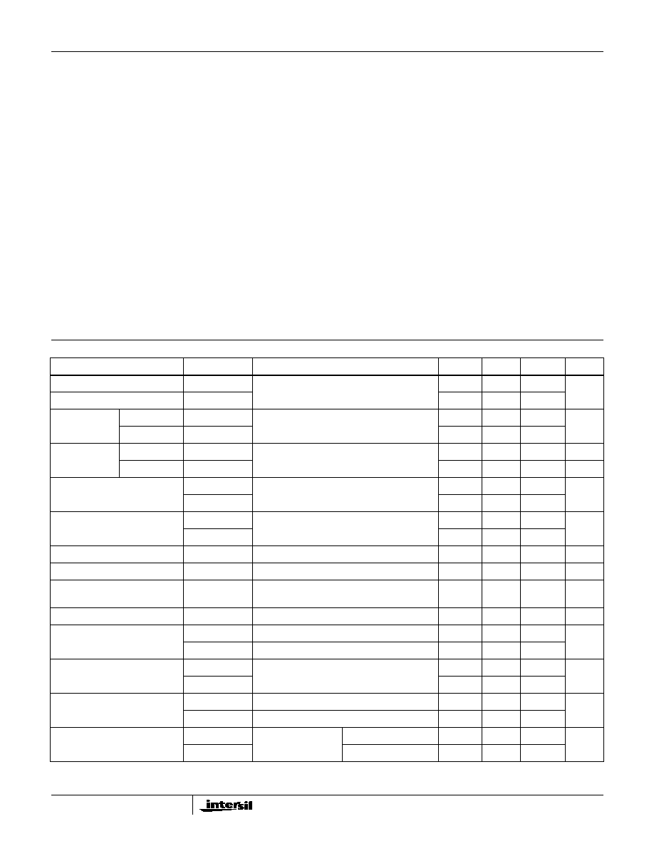
Electrical Specifications
f
C
= 20MSPS, AV
DD
= 3V, DV
DD
= 3V, V
RB
= 1V, V
RT
= 2V, T
A
= 25
o
C
PARAMETER
SYMBOL
CONDITIONS
MIN.
TYP.
MAX.
UNIT
Maximum Conversion Rate
f
C
max
f
IN
=
1.0kHz Triangular Wave Input
20
-
-
MSPS
Minimum Conversion Rate
f
C
min
-
-
0.5
Supply Voltage
Analog
IA
DD
f
IN
=
1.0kHz Triangular Wave Input
-
12
-
mA
Digital
ID
DD
BE = High
-
1.0
-
Standby Current Analog
IA
ST
CE = AV
DD
-
1.0
-
mA
Digital
ID
ST
-
1.0
-
µ
A
Reference Pin Current 1
I
RT1
VRTS, VRBS: Open Between V
RT
and V
RB
-
100
-
µ
A
I
RB1
-
-100
-
Reference Pin Current 2
I
RT2
BE = AV
DD
Between V
RTC
and V
RBC
-
2
-
mA
I
RB2
-
-2
-
Analog Input Band
BW
-1dB
-
TBD
-
MHz
Analog Input Capacitance
C
IN
-
10
-
pF
Reference Resistance Value 1
R
REF1
Between V
RTS
and V
RT
, V
RT
and V
RB
, V
RB
and V
RBS
-
10k
-
Reference Resistance Value 2
R
REF2
Between V
RTC
and V
RBC
-
500
-
Offset Voltage
EOT
EOT = Theoretical Value - Measured Value
-
TBD
-
mV
EOB
EOB = Measured Value - Theoretical Value
-
TBD
-
Digital Input Voltage
V
IH
A
VDD
= 2.7 to 3.3V
0.7
-
-
V
V
IL
-
-
0.2
Analog Input Current
A
IH
V
IN
= 2V
-
20
-
µ
A
A
IL
V
IN
= 1V
-
-20
-
Digital Input Current
I
IH
AV
DD
= 3.3V
V
IH
- AV
DD
-
-
5
µ
A
I
IL
V
IL
= AV
SS
-
-
5
HI3300

4
Digital Output Current
I
OH
OE = AV
SS
DV
DD
= 2.7V
V
OH
= DV
DD
-0.4V
1.0
-
-
mA
I
OL
V
OL
= 0.4V
1.0
-
-
Digital Output Current
I
OZH
OE = AV
DD
DV
DD
= 3.3V
V
OH
= DV
DD
-
-
1.0
µ
A
I
OZL
V
OL
= 0V
-
-
1.0
Three-State Output Disable time
t
PEZ
Clock not Synchronized for Active
High
Impedance
-
2
-
ns
Three-State Output Enable Time
t
PEZ
Clock not Synchronized For High Impedance
Active
-
2
-
ns
Integral Nonlinearity Error
E
L
-
±
1.0
-
LSB
Differential Nonlinearity Error
E
D
-
±
0.5
-
LSB
Differential Gain Error
DG
NTSC 40 IRE Mod Ramp, f
C
= 14.3MSPS
-
TBD
-
%
Differential Phase Error
DP
-
TBD
-
Deg
Output Data Delay
t
DL
C
L
= 20pF
-
3
-
ns
Sampling Delay
t
SD
-
2
-
ns
SNR
SNR
f
IN
= 100kHz
-
TBD
-
dB
f
IN
= 500kHz
-
TBD
-
dB
f
IN
= 1MHz
-
TBD
-
dB
f
IN
= 3MHz
-
TBD
-
dB
f
IN
= 7MHz
-
TBD
-
dB
f
IN
= 10MHz
-
TBD
-
dB
SFDR
SFDR
f
IN
= 100kHz
-
TBD
-
dB
f
IN
= 500kHz
-
TBD
-
dB
f
IN
= 1MHz
-
TBD
-
dB
f
IN
= 3MHz
-
TBD
-
dB
f
IN
= 7MHz
-
TBD
-
dB
f
IN
= 10MHz
-
TBD
-
dB
Electrical Specifications
f
C
= 20MSPS, AV
DD
= 3V, DV
DD
= 3V, V
RB
= 1V, V
RT
= 2V, T
A
= 25
o
C (Continued)
PARAMETER
SYMBOL
CONDITIONS
MIN.
TYP.
MAX.
UNIT
HI3300

