
1
Û
FN7059.2
EL2244, EL2444
Dual/Quad Low-Power 120MHz Unity-Gain
Stable Op Amp
The EL2244 and EL2444 are dual and quad versions of the
popular EL2044. They are high speed, low power, low cost
monolithic operational amplifiers built on Elantec's
proprietary complementary bipolar process. The EL2244
and EL2444 are unity-gain stable and feature a 325V/çs
slew rate and 120MHz gain-bandwidth product while
requiring only 5.2mA of supply current per amplifier.
The power supply operating range of the EL2244 and
EL2444 is from Ý18V down to as little as Ý2V. For single-
supply operation, the EL2244 and EL2444 operate from 36V
down to as little as 2.5V. The excellent power supply
operating range of the EL2244 and EL2444 makes them an
obvious choice for applications on a single +5V or +3V
supply.
The EL2244 and EL2444 also feature an extremely wide
output voltage swing of Ý13.6V with V
S
= Ý15V and R
L
=1k
.
At Ý5V, output voltage swing is a wide Ý3.8V with R
L
= 500
and Ý3.2V with R
L
= 150
. Furthermore, for single-supply
operation at +5V, output voltage swing is an excellent 0.3V
to 3.8V with R
L
= 500
.
At a gain of +1, the EL2244 and EL2444 have a -3dB
bandwidth of 120MHz with a phase margin of 50¯. Because
of their conventional voltage-feedback topology, the EL2244
and EL2444 allow the use of reactive or non-linear elements
in their feedback network. This versatility combined with low
cost and 75mA of output-current drive make the EL2244 and
EL2444 an ideal choice for price-sensitive applications
requiring low power and high speed.
Features
ñ 120MHz gain-bandwidth product
ñ Unity-gain stable
ñ Low supply current (per amplifier)
- 5.2mA at V
S
= Ý15V
ñ Wide supply range - 2.5V to 36V
ñ High slew rate - 325V/çs
ñ Fast settling - 80ns to 0.1% for a 10V step
ñ Low differential gain - 0.04% at A
V
= +2, R
L
= 150
ñ Low differential phase - 0.15¯ at A
V
= +2, R
L
= 150
ñ Wide output voltage swing - Ý13.6V with V
S
= Ý15V,
R
L
= 1k
ñ Low cost, enhanced replacement for the AD827 &
LT1229/LT1230
ñ
Pb-Free available (RoHS compliant)
Applications
ñ Video amplifiers
ñ Single-supply amplifiers
ñ Active filters/integrators
ñ High speed signal processing
ñ ADC/DAC buffers
ñ Pulse/RF amplifiers
ñ Pin diode receivers
ñ Log amplifiers
Pinouts
EL2244
(8-PIN SO, PDIP)
TOP VIEW
EL2444
[14-PIN SO (0.150"), PDIP]
TOP VIEW
1
2
3
4
8
7
6
5
-
+
-
+
OUT
IN1-
IN1+
V-
V+
OUT2
I
N2-
IN2+
1
2
3
4
14
13
12
11
5
6
7
10
9
8
OUT1
IN1-
IN1+
V+
OUT4
IN4-
IN4+
V-
IN2+
IN2-
OUT2
I
N3+
IN3-
OUT3
- +
-
+
- +
-
+
Data Sheet
May 16, 2005
CAUTION: These devices are sensitive to electrostatic discharge; follow proper IC Handling Procedures.
1-888-INTERSIL or 1-888-352-6832
|
Intersil (and design) is a registered trademark of Intersil Americas Inc.
Copyright Intersil Americas Inc. 2004, 2005. All Rights Reserved
All other trademarks mentioned are the property of their respective owners.
NOT
RECO
MME
NDED
FOR
NEW
DES
IGNS
POSS
IBLE
SUB
STITU
TE P
RODU
CTS
(ISL5
5002
, ISL5
5004
)
2
Ordering Information
PART NUMBER
PACKAGE
TAPE &
REEL
PKG.
DWG. #
EL2244CM
16-Pin SO (0.300")
-
MDP0027
EL2244CM-T13
16-Pin SO (0.300")
13"
MDP0027
EL2244CMZ
(See Note)
16-Pin SO (0.300")
(Pb-free)
-
MDP0027
EL2244CMZ-T13
(See Note)
16-Pin SO (0.300")
(Pb-free)
13"
MDP0027
EL2244CN
8-Pin PDIP
-
MDP0031
EL2244CS
8-Pin SO
-
MDP0027
EL2244CS-T7
8-Pin SO
7"
MDP0027
EL2244CS-T13
8-Pin SO
13"
MDP0027
EL2244CSZ
(See Note)
8-Pin SO
(Pb-free)
-
MDP0027
EL2244CSZ-T7
(See Note)
8-Pin SO
(Pb-free)
7"
MDP0027
EL2244CSZ-T13
(See Note)
8-Pin SO
(Pb-free)
13"
MDP0027
EL2444CN
14-Pin PDIP
-
MDP0031
EL2444CS
14-Pin SO (0.150")
-
MDP0027
EL2444CS-T7
14-Pin SO (0.150")
7"
MDP0027
EL2444CS-T13
14-Pin SO (0.150")
13"
MDP0027
EL2444CSZ
(See Note)
14-Pin SO (0.150")
(Pb-free)
-
MDP0027
EL2444CSZ-T7
(See Note)
14-Pin SO (0.150")
(Pb-free)
7"
MDP0027
EL2444CSZ-T13
(See Note)
14-Pin SO (0.150")
(Pb-free)
13"
MDP0027
NOTE: Intersil Pb-free products employ special Pb-free material sets;
molding compounds/die attach materials and 100% matte tin plate
termination finish, which are RoHS compliant and compatible with
both SnPb and Pb-free soldering operations. Intersil Pb-free products
are MSL classified at Pb-free peak reflow temperatures that meet or
exceed the Pb-free requirements of IPC/JEDEC J STD-020.
EL2244, EL2444

3
Absolute Maximum Ratings
(T
A
= 25¯C)
Supply Voltage (V
S
). . . . . . . . . . . . . . . . . . . . . . . . . . . . Ý18V or 36V
Input Voltage (V
IN)
. . . . . . . . . . . . . . . . . . . . . . . . . . . . . . . . . . . ÝV
S
Differential Input Voltage (dV
IN
) . . . . . . . . . . . . . . . . . . . . . . . .Ý10V
Continuous Output Current . . . . . . . . . . . . . . . . . . . . . . . . . . . 40mA
Power Dissipation (P
D
) . . . . . . . . . . . . . . . . . . . . . . . . . See Curves
Operating Temperature Range (T
A
) . . . . . . . . . . . . .-40¯C to +85¯C
Operating Junction Temperature (T
J
) . . . . . . . . . . . . . . . . . . +150¯C
Storage Temperature (T
ST
). . . . . . . . . . . . . . . . . . .-65¯C to +150¯C
CAUTION: Stresses above those listed in "Absolute Maximum Ratings" may cause permanent damage to the device. This is a stress only rating and operation of the
device at these or any other conditions above those indicated in the operational sections of this specification is not implied.
IMPORTANT NOTE: All parameters having Min/Max specifications are guaranteed. Typical values are for information purposes only. Unless otherwise noted, all tests
are at the specified temperature and are pulsed tests, therefore: T
J
= T
C
= T
A
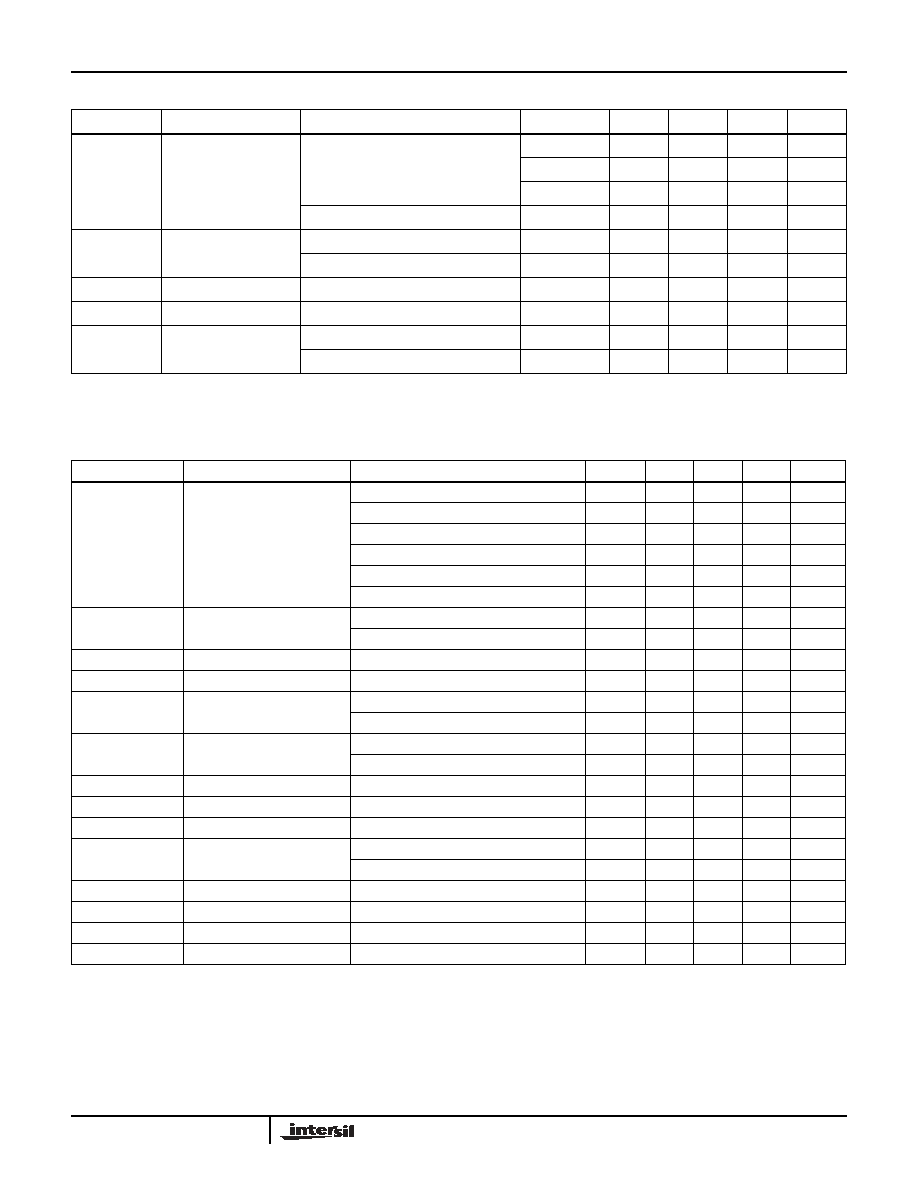
DC Electrical Specifications
V
S
= Ý15V, R
L
= 1k
, unless otherwise specified.
PARAMETER
DESCRIPTION
CONDITION
TEMP
MIN
TYP
MAX
UNIT
V
OS
Input Offset Voltage
V
S
= Ý15V
25¯C
0.5
4.0
mV
T
MIN
, T
MAX
9.0
mV
TCV
OS
Average Offset Voltage
Drift
(Note 1)
All
10.0
çV/¯C
I
B
Input Bias Current
V
S
= Ý15V
25¯C
2.8
8.2
çA
T
MIN
, T
MAX
11.2
çA
V
S
= Ý5V
25¯C
2.8
çA
I
OS
Input Offset Current
V
S
= Ý15V
25¯C
50
300
nA
T
MIN
, T
MAX
500
nA
V
S
= Ý5V
25¯C
50
nA
TCI
OS
Average Offset Current
Drift
(Note 1)
All
0.3
nA/¯C
A
VOL
Open-Loop Gain
V
S
= Ý15V, V
OUT
= Ý10V, R
L
= 1k
25¯C
800
1500
V/V
T
MIN
, T
MAX
600
V/V
V
S
= Ý5V, V
OUT
= Ý2.5V, R
L
= 500
25¯C
1200
V/V
V
S
= Ý5V, V
OUT
= Ý2.5V, R
L
= 150
25¯C
1000
V/V
PSRR
Power Supply Rejection
Ratio
V
S
= Ý5V to Ý15V
25¯C
65
80
dB
T
MIN
, T
MAX
60
dB
CMRR
Common-mode
Rejection Ratio
V
CM
= Ý12V, V
OUT
= 0V
25¯C
70
90
dB
T
MIN
, T
MAX
70
dB
CMIR
Common-mode Input
Range
V
S
= Ý15V
25¯C
Ý14.0
V
V
S
= Ý5V
25¯C
Ý4.2
V
V
S
= +5V
25¯C
4.2/0.1
V
V
OUT
Output Voltage Swing
V
S
= Ý15V, R
L
= 1k
25¯C
Ý13.4
Ý13.6
V
T
MIN
, T
MAX
Ý13.1
V
V
S
= Ý15V, R
L
= 500
25¯C
Ý12.0
Ý13.4
V
V
S
= Ý5V, R
L
= 500
25¯C
Ý3.4
Ý3.8
V
V
S
= Ý5V, R
L
= 150
25¯C
Ý3.2
V
V
S
= +5V, R
L
= 500
25¯C
3.6/0.4
3.8/0.3
V
T
MIN
, T
MAX
3.5/0.5
V
I
SC
Output Short Circuit
Current
25¯C
40
75
mA
T
MIN
, T
MAX
35
mA
EL2244, EL2444
4
I
S
Supply Current
(per amplifier)
V
S
= Ý15V, no load
25¯C
5.2
7
mA
T
MIN
7.6
mA
T
MAX
7.6
mA
V
S
= Ý5V, no load
25¯C
5.0
mA
R
IN
Input Resistance
Differential
25¯C
150
k
Common-mode
25¯C
15
M
C
IN
Input Capacitance
A
V
= +1 @10MHz
25¯C
1.0
pF
R
OUT
Output Resistance
A
V
= +1
25¯C
50
m
PSOR
Power-Supply Operating
Range
Dual-supply
25¯C
Ý2.0
Ý18.0
V
Single-supply
25¯C
2.5
36.0
V
NOTE:
1. Measured from T
MIN
to T
MAX
.
DC Electrical Specifications
V
S
= Ý15V, R
L
= 1k
, unless otherwise specified. (Continued)
PARAMETER
DESCRIPTION
CONDITION
TEMP
MIN
TYP
MAX
UNIT
Closed-Loop AC Electrical Specifications
V
S
= Ý15V, A
V
= +1, R
L
= 1k
, unless otherwise specified.
PARAMETER
DESCRIPTION
CONDITION
TEMP
MIN
TYP
MAX
UNIT
BW
-3dB Bandwidth
(V
OUT
= 0.4V
PP
)
V
S
= Ý15V, A
V
= +1
25¯C
120
MHz
V
S
= Ý15V, A
V
= -1
25¯C
60
MHz
V
S
= Ý15V, A
V
= +2
25¯C
60
MHz
V
S
= Ý15V, A
V
= +5
25¯C
12
MHz
V
S
= Ý15V, A
V
= +10
25¯C
6
MHz
V
S
= Ý5V, A
V
= +1
25¯C
80
MHz
GBWP
Gain-Bandwidth Product
V
S
= Ý15V
25¯C
60
MHz
V
S
= Ý5V
25¯C
45
MHz
PM
Phase Margin
R
L
= 1k
, C
L
= 10pF
25¯C
50
¯
CS
Channel Separation
f = 5MHz
25¯C
85
dB
SR
Slew Rate (Note 1)
V
S
= Ý15V, R
L
= 1k
25¯C
250
325
V/çs
V
S
= Ý5V, R
L
= 500
25¯C
200
V/çs
FPBW
Full-Power Bandwidth
(Note 2)
V
S
= Ý15V
25¯C
4.0
5.2
MHz
V
S
= Ý5V
25¯C
12.7
MHz
t
R
, t
F
Rise Time, Fall Time
0.1V step
25¯C
3.0
ns
OS
Overshoot
0.1V step
25¯C
20
%
t
PD
Propagation Delay
25¯C
2.5
ns
t
S
Settling to +0.1% (A
V
= +1)
V
S
= Ý15V, 10V step
25¯C
80
ns
V
S
= Ý5V, 5V step
25¯C
60
ns
dG
Differential Gain (Note 3)
NTSC/PAL
25¯C
0.04
%
dP
Differential Phase (Note 3)
NTSC/PAL
25¯C
0.15
¯
eN
Input Noise Voltage
10kHz
25¯C
15.0
nV/
Hz
iN
Input Noise Current
10kHz
25¯C
1.50
pA/
Hz
NOTES:
1. Slew rate is measured on rising edge
2. For V
S
= Ý15V, V
OUT
= 20V
PP
. For V
S
= Ý5V, V
OUT
= 5V
PP
. Full-power bandwidth is based on slew rate measurement using: FPBW = SR /
(2
* Vpeak).
3. Video performance measured at V
S
= Ý15V, A
V
= +2 with 2 times normal video level across R
L
= 150
. This corresponds to standard video
levels across a back-terminated 75
load. For other values of R
L
, see curves.
EL2244, EL2444
5
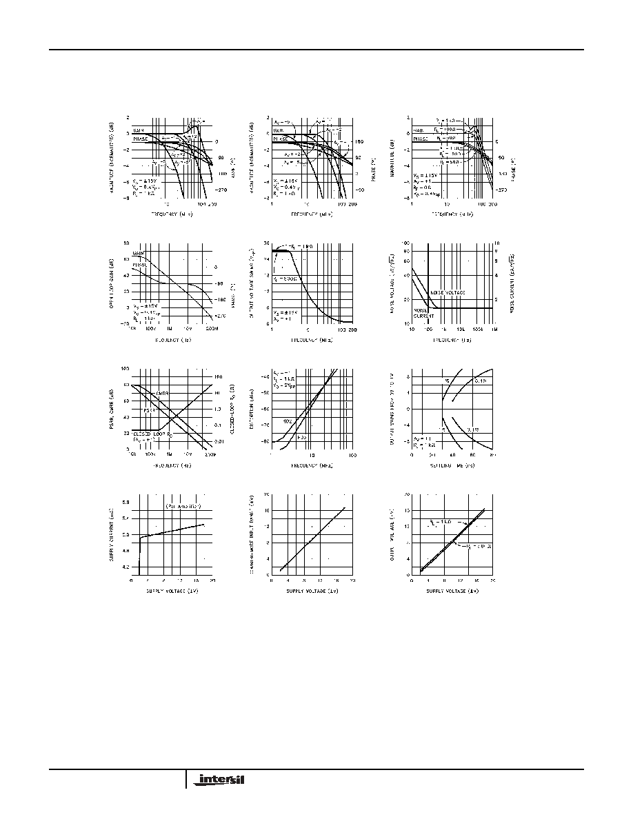
Typical Performance Curves
Non-Inverting
Frequency Response
Inverting Frequency Response
Frequency Response for
Various Load Resistances
Equivalent Input Noise
Settling Time vs
Output Voltage Change
2nd and 3rd Harmonic
Distortion vs Frequency
CMRR, PSRR and Closed-Loop
Output Resistance vs Frequency
Open-Loop Gain and
Phase vs Frequency
Output Voltage Swing
vs Frequency
Common-Mode Input Range
vs Supply Voltage
Supply Current vs
Supply Voltage
Output Voltage Range
vs Supply Voltage
EL2244, EL2444