1
®
EL2082
Data Sheet
January 1996, Rev.D
FN7152
Current Mode Multiplier
The EL2082 is a general purpose
variable gain control building block,
built using an advanced proprietary
complementary bipolar process. It is a two-quandrant
multiplier, so that zero or negative control voltages do not
allow signal feedthrough and very high attenuation is
possible. The EL2082 works in current mode rather than
voltage mode, so that the input impedance is low and the
output impedance is high. This allows very wide bandwidth
for both large and small signals.
The I
IN
pin replicates the voltage present on the V
IN
pin;
therefore, the V
IN
pin can be used to reject common-mode
noise and establish an input ground reference. The gain
control input is calibrated to 1mA/mA signal gain for 1V of
control voltage. The disable pin (E) is TTL-compatible, and
the output current can comply with a wide range of output
voltages.
Because current signals rather than voltages are employed,
multiple inputs can be summed and many outputs wire-or'ed
or mixed.
The EL2082 operates from a wide range of supplies and is
available in standard 8-pin plastic DIP or 8-pin SO.
Features
· Flexible inputs and outputs, all ground referred
· 150MHz large and small-signal bandwidth
· 46dB of calibrated gain control range
· 70dB isolation in disable mode @ 10MHz
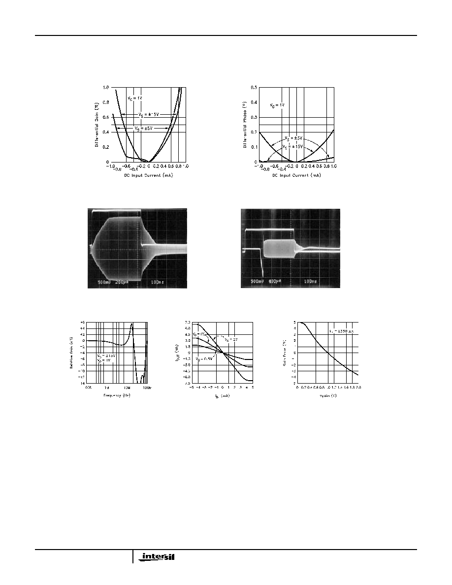
· 0.15% diff gain and 0.05° diff phase performance at NTSC
using application circuit
· Operates on ±5V to ±15V power supplies
· Outputs may be paralleled to function as a multiplexer
Applications
· Level adjust for video signals
· Video faders and mixers
· Signal routing multiplexers
· Variable active filters
· Video monitor contrast control
· AGC
· Receiver IF gain control
· Modulation/demodulation
· General "cold" front-panel control of AC signals
EL2082
(8-PIN SO, PDIP)
TOP VIEW
Ordering Information
PART
NUMBER
TEMP. RANGE
PACKAGE
PKG. NO.
EL2082CN
0°C to +75°C
8-Pin PDIP
MDP0031
EL2082CS
0°C to +75°C
8-Pin SO
MDP0027
CAUTION: These devices are sensitive to electrostatic discharge; follow proper IC Handling Procedures.
1-888-INTERSIL or 321-724-7143
|
Intersil (and design) is a registered trademark of Intersil Americas Inc.
Copyright © Intersil Americas Inc. 2003. All Rights Reserved. Elantec is a registered trademark of Elantec Semiconductor, Inc.
All other trademarks mentioned are the property of their respective owners.
OBSO
LETE
PRO
DUCT
NO R
ECOM
MEND
ED R
EPLA
CEME
NT
conta
ct ou
r Tec
hnica
l Sup
port C
enter
at
1-888
-INTE
RSIL
or w
ww.in
tersil
.com
/tsc
2
EL2082
Absolute Maximum Ratings
(T
A
= 25°C)
V
S
Voltage between V
S
+ and V
S
- . . . . . . . . . . . . . . .+33V
V
IN
, V
OUT
Voltage . . . . . . . . . . . . . . . . . . . . . . . . . . . . . . . . . ±V
S
V
E
, V
GAIN
Input Voltage . . . . . . . . . . . . . . . . . . . . . . . . -1 to +7V
I
IN
Input Current . . . . . . . . . . . . . . . . . . . . . . . . . . . ±5mA
P
D
Maximum Power Dissipation . . . . . . . . . . See Curves
T
A
Operating Temperature Range . . . . . . . 0°C to +75°C
T
J
Operating Junction Temperature . . . . . . . . . . . . 150°C
T
ST
Storage Temperature . . . . . . . . . . . . . -65°C to +150°C
CAUTION: Stresses above those listed in "Absolute Maximum Ratings" may cause permanent damage to the device. This is a stress only rating and operation of the
device at these or any other conditions above those indicated in the operational sections of this specification is not implied.
IMPORTANT NOTE: All parameters having Min/Max specifications are guaranteed. Typical values are for information purposes only. Unless otherwise noted, all tests
are at the specified temperature and are pulsed tests, therefore: T
J
= T
C
= T
A
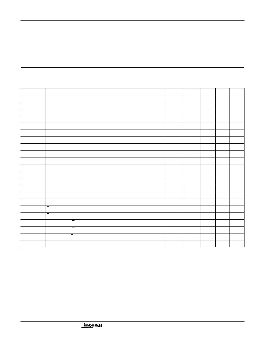
DC Electrical Specifications
V
S
= ±15V, V
G
= 1V, V
E
= 0.8V, V
OUT
= 0, V
IN
= 0, I
IN
= 0
PARAMETER
DESCRIPTION
TEMP
MIN
TYP
MAX
UNITS
V
IO
Input Offset Voltage
Full
-20
20
mV
I
OO
Output Offset Current
Full
-100
100
µA
R
INI
I
IN
Input Impedance; I
IN
= 0, 0.35mA
Full
75
95
115
V
CMRR
Voltage Common-Mode Rejection Ratio, V
IN
= -10V, +10V
Full
45
55
dB
I
CMRR
Offset Current Common-Mode Rejection Ratio, V
IN
= -10V, +10V
Full
0.5
5
µA/V
V
PSRR
Offset Voltage Power Supply Rejection Ratio, V
S
= ±5V to ±15V
Full
60
80
dB
I
PSRR
Offset Current Power Supply Rejection Ratio, V
S
= ±5V to ±15V
Full
1
10
µA/V
I
BVIN
V
IN
Bias Current
Full
-10
10
µA
R
INV
V
IN
Input Impedance; V
IN
= -10V, +10V
Full
0.5
1.0
M
Nlini
Signal Nonlinearity; I
IN
= -0.7mA, -0.35mA, 0mA, +0.35mA, +0.7mA
Full
0.10
0.4
%
R
OUT
Output Impedance V
OUT
= -10V, +10V
Full
0.25
0.5
M
V
OUT
Output Swing; V
GAIN
= 2V, I
IN
±2 mA, R
L
= 4.0k
Full
-11
+11
V
V
IOG
V
OS
, Gain Control, Extrapolated from V
GAIN
= 0.1V, 1V
Full
-15
15
mV
A
I
Current Gain, I
IN
±350µA
Full
0.9
1.0
1.1
mA/mA
Nling
Nonlinearity of Gain Control, V
GAIN
= 0.1V, 0.5V, 1V
Full
2
5
%
I
SO
Input Isolation with V
GAIN
= -0.1V
Full
-80
-96
dB
V
INH
E Logic High Level
Full
2.0
V
V
INL
E Logic Low Level
Full
0.8
V
I
LH
Input Current of E, V
E
= 5V
Full
-50
50
µA
I
LL
Input Current of E, V
E
= 0
Full
-50
50
µA
I
ODIS
I
OUT
, Disabled E = 2.0V
Full
±10
µA
I
S
Supply Current
Full
13
16
mA