CAUTION: These devices are sensitive to electrostatic discharge. Users should follow proper I.C. Handling Procedures.
Copyright
©
Harris Corporation 1994
1
S E M I C O N D U C T O R
CD54AC163/3A
CD54ACT163/3A
Synchronous Presettable Binary Counters
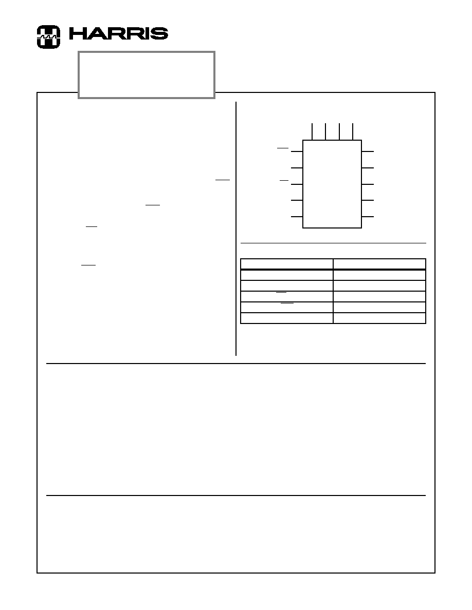
Functional Diagram
ACT INPUT LOAD TABLE
INPUT
UNIT LOAD (NOTE 1)
Pn
0.13
CP
1
MR, TE
0.83
SPE
0.67
PE
0.5
NOTE:
1. Unit load is
I
CC
limit specified in DC Electrical Specifications
Table, e.g., 2.4mA Max at +25
o
C.
SPE
CP
MR
PE
TE
9
2
1
7
10
GND = 8
V
CC
= 16
3
4
5
6
14
13
12
11
15
Q0
Q1
Q2
Q3
TC
P0
P1
P2
P3
June 1997
File Number
3893
Description
The CD54AC163/3A and CD54ACT163/3A are synchronous
presettable binary counters that utilize the Harris Advanced
CMOS Logic technology. The CD54AC163/3A and
CD54ACT163/3A are reset synchronously with the clock.
Counting and parallel presetting are both accomplished syn-
chronously with the negative-to-positive transition of the
clock.
A LOW level on the Synchronous Parallel Enable input, SPE,
disables the counting operation and allows data at the P0 to
P3 inputs to be loaded into the counter (provided that the
setup and hold requirements for SPE are met).
The counters are reset with a LOW level on the Master
Reset input, MR. The requirements for setup and hold time
with respect to the clock must be met.
Two count enables, PE and TE, in each counter are provided
for n-bit cascading. Reset action occurs regardless of the
level of the SPE, PE and TE inputs.
The look-ahead carry feature simplifies serial cascading of
the counters. Both count enable inputs (PE and TE) must be
HIGH to count. The TE input is gated with the Q outputs of
all four stages so that at the maximum count, the terminal
count (TC) output goes HIGH for one clock period. This TC
pulse is used to enable the next cascaded stage.
The CD54AC163/3A and CD54ACT163/3A are supplied in
16 lead dual-in-line ceramic packages (F suffix).
Absolute Maximum Ratings
DC Supply Voltage, V
CC
. . . . . . . . . . . . . . . . . . . . . . . . -0.5V to +6V
DC Input Diode Current, I
IK
For V
I
< -0.5V or V
I
> V
CC
+ 0.5V
. . . . . . . . . . . . . . . . . . . . . .±
20mA
DC Output Diode Current, I
OK
For V
O
< -0.5V or V
O
> V
CC
+ 0.5V
. . . . . . . . . . . . . . . . . . . . .±
50mA
DC Output Source or Sink Current, Per Output Pin, I
O
For V
O
> -0.5V or V
O
< V
CC
+ 0.5V
. . . . . . . . . . . . . . . . . . . . .±
50mA
DC V
CC
or GND Current, I
CC
or I
GND
For Up to 4 Outputs Per Device, Add
±
25mA For Each
Additional Output
. . . . . . . . . . . . . . . . . . . . . . . . . . . . . . . . . . .±
100mA
Power Dissipation Per Package, P
D
T
A
= -55
o
C to +100
o
C (Package F) . . . . . . . . . . . . . . . . . . 500mW
T
A
= +100
o
C to +125
o
C (Package F) . . . . . . . . Derate Linearly at
8mW/
o
C to 300mW
Operating Temperature Range, T
A
Package Type F . . . . . . . . . . . . . . . . . . . . . . . . . . -55
o
C to +125
o
C
Storage Temperature, T
STG
. . . . . . . . . . . . . . . . . . -65
o
C to +150
o
C
Lead Temperature (During Soldering)
At Distance 1/16in.
±
1/32in. (1.59mm
±
0.79mm)
From Case For 10s Max . . . . . . . . . . . . . . . . . . . . . . . . . . +265
o
C
Unit Inserted Into a PC Board (Min Thickness 1/16in., 1.59mm)
With Solder Contacting Lead Tips Only. . . . . . . . . . . . . . . +300
o
C
CAUTION: Stresses above those listed in "Absolute Maximum Ratings" may cause permanent damage to the device. This is a stress only rating and operation
of the device at these or any other conditions above those indicated in the operational sections of this specification is not implied.
Recommended Operating Conditions
Supply Voltage Range, V
CC
Unless Otherwise Specified, All Voltages Referenced to GND
T
A
= Full Package Temperature Range
CD54AC Types . . . . . . . . . . . . . . . . . . . . . . . . . . . . . .1.5V to 5.5V
CD54ACT Types . . . . . . . . . . . . . . . . . . . . . . . . . . . . .4.5V to 5.5V
DC Input or Output Voltage, V
I
, V
O
. . . . . . . . . . . . . . . . . . 0V to V
CC
Operating Temperature, T
A
. . . . . . . . . . . . . . . . . . . -55
o
C to +125
o
C
Input Rise and Fall Slew Rate, dt/dv
at 1.5V to 3V (AC Types) . . . . . . . . . . . . . . . . . . . 0ns/V to 50ns/V
at 3.6V to 5.5V (AC Types) . . . . . . . . . . . . . . . . . 0ns/V to 20ns/V
at 4.5V to 5.5V (AC Types) . . . . . . . . . . . . . . . . . 0ns/V to 10ns/V
COMING SOON!
COMPLETE DATA SHEET