
7-1169
CAUTION: These devices are sensitive to electrostatic discharge; follow proper IC Handling Procedures.
1-888-INTERSIL or 321-724-7143 | Copyright © Intersil Corporation 1999
CD4511BMS
CMOS BCD-to-7-Segment
Latch Decoder Drivers
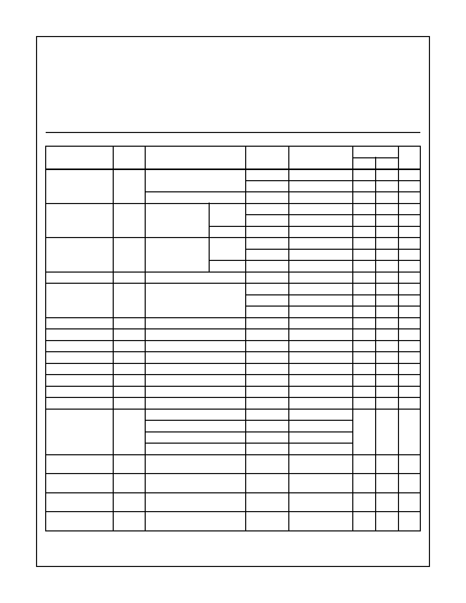
Pinout
CD4511BMS
TOP VIEW
Functional Diagram
7-Segment Display
14
15
16
9
13
12
11
10
1
2
3
4
5
7
6
8
B
C
LT
BL
LE/STROBE
D
VSS
A
VDD
g
a
b
c
d
e
f
L
A
T
C
H
D
E
C
O
D
E
R
D
R
I
V
E
R
13
12
11
10
9
15
14
a
b
c
d
e
f
g
7
1
2
6
A
B
C
D
7
SEGMENT
OUTPUTS
BCD
INPUTS
BL
4
LE/STROBE
5
LT
3
VSS = 8
VDD = 16
a
b
c
d
g
f
e
Features
· High Voltage Type (20V Rating)
· High Output Sourcing Capability up to 25mA
· Input Latches for BCD Code Storage
· Lamp Test and Blanking Capability
· 7 Segment Outputs Blanked for BCD Input Codes
> 1001
· 100% Tested for Quiescent Current at 20V
· 5V, 10V and 15V Parametric Ratings
· Maximum Input Current of 1
µ
A at 18V Over Full Pack-
age Temperature Range; 100nA at 18V and +25
o
C
Applications
· Driving Common Cathode LED Displays
· Multiplexing with Common Cathode LED Displays
· Driving Incandescent Displays
· Driving Low Voltage Fluorescent Displays
Description
CD4511BMS is a BCD-to-7-Segment latch decoder drivers
constructed with CMOS logic and n-p-n bipolar transistor
output devices on a single monolithic structure. These
devices combine the low quiescent power dissipation and
high noise immunity features of Intersil CMOS with n-p-n
bipolar output transistors capable of sourcing up to 25mA.
This capability allows the CD4511BMS types to drive LED's
and other displays directly.
Lamp Test (LT), Blanking (BL), and Latch Enable or Strobe
inputs are provided to test the display, shut off or intensity
modulate it, and store or strobe a BCD code, respectively.
Several different signals may be multiplexed and displayed
when external multiplexing circuitry is used.
These devices are similar to the type MC14511.
The CD4511BMS is supplied in these 16-lead outline
packages:
Braze Seal DIP
H4W
Frit Seal DIP
H2R
Ceramic Flatpack
H6W
December 1992
File Number
3339
7-1170
Specifications CD4511BMS
Absolute Maximum Ratings
Reliability Information
DC Supply Voltage Range, (VDD) . . . . . . . . . . . . . . . -0.5V to +20V
(Voltage Referenced to VSS Terminals)
Input Voltage Range, All Inputs . . . . . . . . . . . . .-0.5V to VDD +0.5V
DC Input Current, Any One Input
. . . . . . . . . . . . . . . . . . . . . . . .±
10mA
Operating Temperature Range . . . . . . . . . . . . . . . . -55
o
C to +125
o
C
Package Types D, F, K, H
Storage Temperature Range (TSTG) . . . . . . . . . . . -65
o
C to +150
o
C
Lead Temperature (During Soldering) . . . . . . . . . . . . . . . . . +265
o
C
At Distance 1/16
±
1/32 Inch (1.59mm
±
0.79mm) from case for
10s Maximum
Thermal Resistance . . . . . . . . . . . . . . . .
ja
jc
Ceramic DIP and FRIT Package . . . . .
80
o
C/W
20
o
C/W
Flatpack Package . . . . . . . . . . . . . . . .
70
o
C/W
20
o
C/W
Maximum Package Power Dissipation (PD) at +125
o
C
For T
A
= -55
o
C to +100
o
C (Package Type D, F, K) . . . . . . 500mW
For T
A
= +100
o
C to +125
o
C (Package Type D, F, K). . . . . . Derate
Linearity at 12mW/
o
C to 200mW
Device Dissipation per Output Transistor . . . . . . . . . . . . . . . 100mW
For T
A
= Full Package Temperature Range (All Package Types)
Junction Temperature . . . . . . . . . . . . . . . . . . . . . . . . . . . . . . +175
o
C
TABLE 1. DC ELECTRICAL PERFORMANCE CHARACTERISTICS
PARAMETER
SYMBOL
CONDITIONS (NOTE 1)
GROUP A
SUBGROUPS
TEMPERATURE
LIMITS
UNITS
MIN
MAX
Supply Current
IDD
VDD = 20V, VIN = VDD or GND
1
+25
o
C
-
10
µ
A
2
+125
o
C
-
1000
µ
A
VDD = 18V, VIN = VDD or GND
3
-55
o
C
-
10
µ
A
Input Leakage Current
IIL
VIN = VDD or GND
VDD = 20
1
+25
o
C
-100
-
nA
2
+125
o
C
-1000
-
nA
VDD = 18V
3
-55
o
C
-100
-
nA
Input Leakage Current
IIH
VIN = VDD or GND
VDD = 20
1
+25
o
C
-
100
nA
2
+125
o
C
-
1000
nA
VDD = 18V
3
-55
o
C
-
100
nA
Output Voltage
VOL15
VDD = 15V, No Load
1, 2, 3
+25
o
C, +125
o
C, -55
o
C
-
50
mV
Output Voltage
VOH15
VDD = 15V, No Load (Note 3)
1
+25
o
C
14.1
-
V
2
+125
o
C
14.2
V
3
-55
o
C
14.0
V
Output Current (Sink)
IOL5
VDD = 5V, VOUT = 0.4V
1
+25
o
C
1
-
mA
Output Current (Sink)
IOL10
VDD = 10V, VOUT = 0.5V
1
+25
o
C
2.6
-
mA
Output Current (Sink)
IOL15
VDD = 15V, VOUT = 1.5V
1
+25
o
C
6.8
-
mA
Output Drive Voltage
LVOH5
VDD = 5V, IOH = -20mA
1
+25
o
C
3.4
-
V
Output Drive Voltage
LVOH10
VDD = 10V, IOH = -20mA
1
+25
o
C
8.6
-
V
Output Drive Voltage
LVOH15
VDD = 15V, IOH = -20mA
1
+25
o
C
13.7
-
V
N Threshold Voltage
VNTH
VDD = 10V, ISS = -10
µ
A
1
+25
o
C
-2.8
-0.7
V
P Threshold Voltage
VPTH
VSS = 0V, IDD = 10
µ
A
1
+25
o
C
0.7
2.8
V
Functional
F
VDD = 2.8V, VIN = VDD or GND
7
+25
o
C
VOH >
VDD/2
VOL <
VDD/2
V
VDD = 20V, VIN = VDD or GND
7
+25
o
C
VDD = 18V, VIN = VDD or GND
8A
+125
o
C
VDD = 3V, VIN = VDD or GND
8B
-55
o
C
Input Voltage Low
(Note 2)
VIL
VDD = 5V, VOH > 3.6V, VOL < 0.5V
1, 2, 3
+25
o
C, +125
o
C, -55
o
C
-
1.5
V
Input Voltage High
(Note 2)
VIH
VDD = 5V, VOH > 3.6V, VOL < 0.5V
1, 2, 3
+25
o
C, +125
o
C, -55
o
C
3.5
-
V
Input Voltage Low
(Note 2)
VIL
VDD = 15V, VOH > 12.6V,
VOL < 1.5V
1, 2, 3
+25
o
C, +125
o
C, -55
o
C
-
4
V
Input Voltage High
(Note 2)
VIH
VDD = 15V, VOH > 12.6V,
VOL < 1.5V
1, 2, 3
+25
o
C, +125
o
C, -55
o
C
11
-
V
NOTES: 1. All voltages referenced to device GND, 100% testing being
implemented.
2. Go/No Go test with limits applied to inputs.
3. For accuracy, voltage is measured differentially to VDD

7-1171
Specifications CD4511BMS
TABLE 2. AC ELECTRICAL PERFORMANCE CHARACTERISTICS
PARAMETER
SYMBOL
CONDITIONS (NOTE 1, 2)
GROUP A
SUBGROUPS
TEMPERATURE
LIMITS
UNITS
MIN
MAX
Propagation Delay
Data to Output
TPHL
VDD = 5V, VIN = VDD or GND
9
+25
o
C
-
1040
ns
10, 11
+125
o
C, -55
o
C
-
1404
ns
Propagation Delay
Data to Output
TPLH
VDD = 5V, VIN = VDD or GND
9
+25
o
C
-
1320
ns
10, 11
+125
o
C, -55
o
C
-
1782
ns
Transition Time
TTHL
VDD = 5V, VIN = VDD or GND
9
+25
o
C
-
310
ns
10, 11
+125
o
C, -55
o
C
-
419
ns
Transition Time
TTLH
VDD = 5V, VIN = VDD or GND
9
+25
o
C
-
80
ns
10, 11
+125
o
C, -55
o
C
-
108
ns
NOTES:
1. CL = 50pF, RL = 200K, Input TR, TF < 20ns.
2. -55
o
C and +125
o
C limits guaranteed, 100% testing being implemented.
TABLE 3. ELECTRICAL PERFORMANCE CHARACTERISTICS
PARAMETER
SYMBOL
CONDITIONS
NOTES
TEMPERATURE
LIMITS
UNITS
MIN
MAX
Supply Current
IDD
VDD = 5V, VIN = VDD or GND
1, 2
-55
o
C, +25
o
C
-
5
µ
A
+125
o
C
-
150
µ
A
VDD = 10V, VIN = VDD or GND
1, 2
-55
o
C, +25
o
C
-
10
µ
A
+125
o
C
-
300
µ
A
VDD = 15V, VIN = VDD or GND
1, 2
-55
o
C, +25
o
C
-
10
µ
A
+125
o
C
-
600
µ
A
Output Voltage
VOL
VDD = 5V, No Load
1, 2
+25
o
C, +125
o
C,
-55
o
C
-
50
mV
Output Voltage
VOL
VDD = 10V, No Load
1, 2
+25
o
C, +125
o
C,
-55
o
C
-
50
mV
Output Voltage
VOH
VDD = 5V, No Load
1, 2
+25
o
C
4.1
-
V
1, 2
+125
o
C
4.2
-
V
1, 2
-55
o
C
4.0
-
V
Output Voltage
VOH
VDD = 10V, No Load
1, 2
+25
o
C
9.1
-
V
1, 2
+125
o
C
9.2
-
V
1, 2
-55
o
C
9.0
-
V
Output Current (Sink)
IOL5
VDD = 5V, VOUT = 0.4V
1, 2
+125
o
C
0.36
-
mA
-55
o
C
0.64
-
mA
Output Current (Sink)
IOL10
VDD = 10V, VOUT = 0.5V
1, 2
+125
o
C
0.9
-
mA
-55
o
C
1.6
-
mA
Output Current (Sink)
IOL15
VDD = 15V, VOUT = 1.5V
1, 2
+125
o
C
2.4
-
mA
-55
o
C
4.2
-
mA
Input Voltage Low
VIL
VDD = 10V, VOH > 9V, VOL < 1V
1, 2
+25
o
C, +125
o
C,
-55
o
C
-
3
V
Input Voltage High
VIH
VDD = 10V, VOH > 9V, VOL < 1V
1, 2
+25
o
C, +125
o
C,
-55
o
C
+7
-
V
Propagation Delay
Data to Output
TPHL
VDD = 10V
1, 2, 3
+25
o
C
-
420
ns
VDD = 15V
1, 2, 3
+25
o
C
-
300
ns

7-1172
Specifications CD4511BMS
Propagation Delay
Data to Output
TPLH
VDD = 10V
1, 2, 3
+25
o
C
-
520
ns
VDD = 15V
1, 2, 3
+25
o
C
-
360
ns
Propagation Delay
(BT)
TPHL
VDD = 5V
1, 2, 3
+25
o
C
-
700
ns
VDD = 10V
1, 2, 3
+25
o
C
-
350
ns
VDD = 15V
1, 2, 3
+25
o
C
-
250
ns
Propagation Delay
(BT)
TPLH
VDD = 5V
1, 2, 3
+25
o
C
-
800
ns
VDD = 10V
1, 2, 3
+25
o
C
-
350
ns
VDD = 15V
1, 2, 3
+25
o
C
-
300
ns
Propagation Delay
(LT)
TPHL
VDD = 5V
1, 2, 3
+25
o
C
-
500
ns
VDD = 10V
1, 2, 3
+25
o
C
-
250
ns
VDD = 15V
1, 2, 3
+25
o
C
-
170
ns
Propagation Delay
(LT)
TPLH
VDD = 5V
1, 2, 3
+25
o
C
-
300
ns
VDD = 10V
1, 2, 3
+25
o
C
-
150
ns
VDD = 15V
1, 2, 3
+25
o
C
-
100
ns
Transition Time
TTHL
VDD = 10V
1, 2, 3
+25
o
C
-
185
ns
VDD = 15V
1, 2, 3
+25
o
C
-
160
ns
Transition Time
TTLH
VDD = 10V
1, 2, 3
+25
o
C
-
60
ns
VDD = 15V
1, 2, 3
+25
o
C
-
50
ns
Minimum Data Setup
Time
TS
VDD = 5V
1, 2, 3
+25
o
C
-
150
ns
VDD = 10V
1, 2, 3
+25
o
C
-
70
ns
VDD = 15V
1, 2, 3
+25
o
C
-
40
ns
Minimum Data Hold Time
TH
VDD = 5V
1, 2, 3
+25
o
C
-
0
ns
VDD = 10V
1, 2, 3
+25
o
C
-
0
ns
VDD = 15V
1, 2, 3
+25
o
C
-
0
ns
Minimum Strobe Pulse
Width
TW
VDD = 5V
1, 2, 3
+25
o
C
-
400
ns
VDD = 10V
1, 2, 3
+25
o
C
-
160
ns
VDD = 15V
1, 2, 3
+25
o
C
-
100
ns
Output Drive Voltage
LVOH5
VDD = 5V, IOH = -10mA
1, 2
+25
o
C
3.9
-
V
1, 2
+125
o
C
3.9
-
V
1, 2
-55
o
C
3.8
-
V
VDD = 5V, IOH = -20mA
1, 2
-55
o
C
3.55
-
V
VDD = 5V, IOH = -25mA
1, 2
+25
o
C
3.1
-
V
1, 2
-55
o
C
3.4
-
V
Output Drive Voltage
LVOH10
VDD = 10V, IOH = -10mA
1, 2
+25
o
C
9.0
-
V
1, 2
+125
o
C
9.0
-
V
1, 2
-55
o
C
8.85
-
V
VDD = 10V, IOH = -20mA
1, 2
+125
o
C
8.4
-
V
1, 2
-55
o
C
8.7
-
V
VDD = 10V, IOH = -25mA
1, 2
+25
o
C
8.3
-
V
1, 2
-55
o
C
8.6
-
V
TABLE 3. ELECTRICAL PERFORMANCE CHARACTERISTICS(Continued)
PARAMETER
SYMBOL
CONDITIONS
NOTES
TEMPERATURE
LIMITS
UNITS
MIN
MAX
7-1173
Specifications CD4511BMS
Output Drive Voltage
LVOH15
VDD = 15V, IOH = -10mA
1, 2
+25
o
C
14.0
-
V
1, 2
+125
o
C
14.0
-
V
1, 2
-55
o
C
13.9
-
V
VDD = 15V, IOH = -20mA
1, 2
+125
o
C
13.5
-
V
1, 2
-55
o
C
13.75
-
V
VDD = 15V, IOH = -25mA
1, 2
+25
o
C
13.5
-
V
1, 2
-55
o
C
13.65
-
V
Input Capacitance
CIN
Any Input
1, 2
+25
o
C
-
7.5
pF
NOTES:
1. All voltages referenced to device GND.
2. The parameters listed on Table 3 are controlled via design or process and are not directly tested. These parameters are characterized
on initial design release and upon design changes which would affect these characteristics.
3. CL = 50pF, RL = 200K, Input TR, TF < 20ns.
TABLE 4. POST IRRADIATION ELECTRICAL PERFORMANCE CHARACTERISTICS
PARAMETER
SYMBOL
CONDITIONS
NOTES
TEMPERATURE
LIMITS
UNITS
MIN
MAX
Supply Current
IDD
VDD = 20V, VIN = VDD or GND
1, 4
+25
o
C
-
25
µ
A
N Threshold Voltage
VNTH
VDD = 10V, ISS = -10
µ
A
1, 4
+25
o
C
-2.8
-0.2
V
N Threshold Voltage
Delta
VTN
VDD = 10V, ISS = -10
µ
A
1, 4
+25
o
C
-
±
1
V
P Threshold Voltage
VTP
VSS = 0V, IDD = 10
µ
A
1, 4
+25
o
C
0.2
2.8
V
P Threshold Voltage
Delta
VTP
VSS = 0V, IDD = 10
µ
A
1, 4
+25
o
C
-
±
1
V
Functional
F
VDD = 18V, VIN = VDD or GND
1
+25
o
C
VOH >
VDD/2
VOL <
VDD/2
V
VDD = 3V, VIN = VDD or GND
Propagation Delay Time
TPHL
TPLH
VDD = 5V
1, 2, 3, 4
+25
o
C
-
1.35 x
+25
o
C
Limit
ns
NOTES: 1. All voltages referenced to device GND.
2. CL = 50pF, RL = 200K, Input TR, TF < 20ns.
3. See Table 2 for +25
o
C limit.
4. Read and Record
TABLE 5. BURN-IN AND LIFE TEST DELTA PARAMETERS +25
o
C
PARAMETER
SYMBOL
DELTA LIMIT
Supply Current - MSI-2
IDD
±
1.0
µ
A
Output Current (Sink)
IOL5
±
20% x Pre-Test Reading
Output Current (Source)
IOH5A
±
20% x Pre-Test Reading
TABLE 6. APPLICABLE SUBGROUPS
CONFORMANCE GROUP
MIL-STD-883
METHOD
GROUP A SUBGROUPS
READ AND RECORD
Initial Test (Pre Burn-In)
100% 5004
1, 7, 9
IDD, IOL5, IOH5A
Interim Test 1 (Post Burn-In)
100% 5004
1, 7, 9
IDD, IOL5, IOH5A
Interim Test 2 (Post Burn-In)
100% 5004
1, 7, 9
IDD, IOL5, IOH5A
TABLE 3. ELECTRICAL PERFORMANCE CHARACTERISTICS(Continued)
PARAMETER
SYMBOL
CONDITIONS
NOTES
TEMPERATURE
LIMITS
UNITS
MIN
MAX