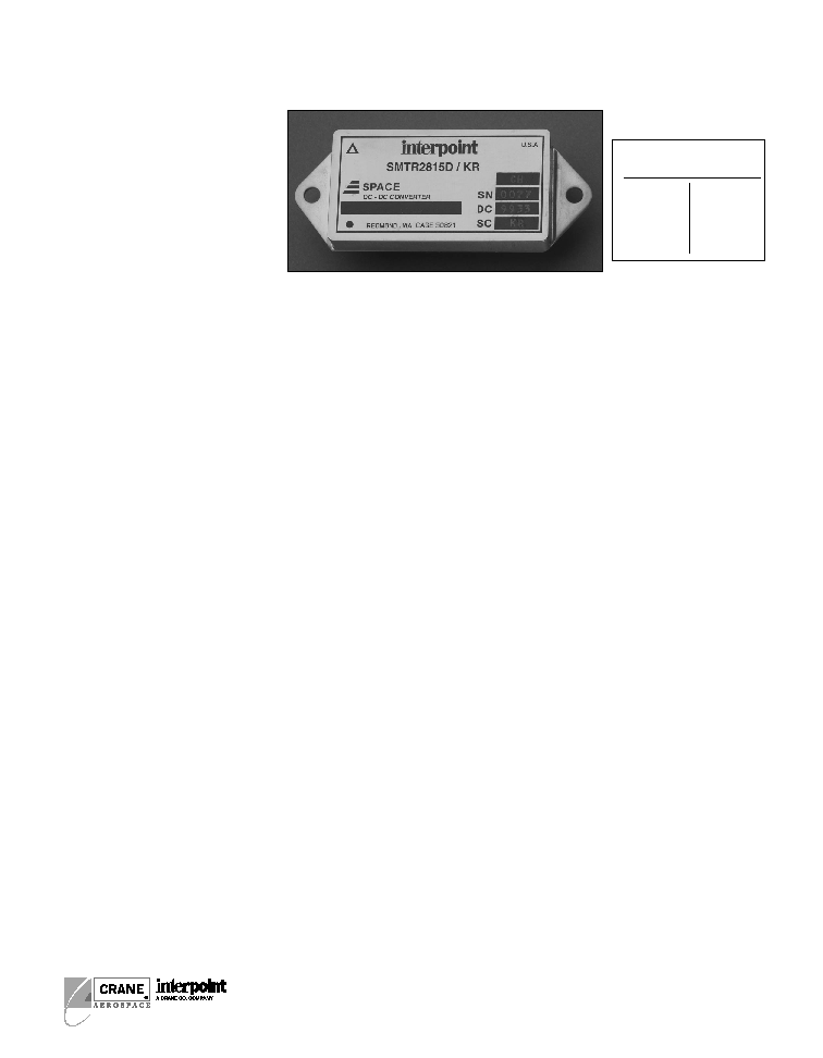
1
MODELS
VDC O
UTPUT
SINGLE
3.3
5
12
15
DUAL
±5
±12
±15
DC/DC C
ONVERTERS
28 V
OLT
I
NPUT
SMTR SERIES
30 WATT
DESCRIPTION
The SMTR SeriesTM of 28 volt DC/DC converters offers up to
30 watts of output power from single or dual output configurations.
The operate over the full military temperature range of 55°C to
+125°C with up to 84% efficiency. SMTR converters are packaged
in hermetically sealed metal enclosures, making them ideal for use
in military, aerospace and other high reliability applications.
S
CREENING AND
R
EPORTS
SMTR converters offer three screening options (Standard, Class H,
or Class K) and two levels of radiation hardness (O or R). See
Tables 1, 2, and 3 for more information. Detailed reports on product
performance are also available and are listed in Table 4.
C
ONVERTER
D
ESIGN
The SMTR converters are constant frequency, pulse-width mod-
ulated switching regulators which use a quasi-square wave, single
ended, forward converter design. Tight load regulation is maintained
by using a wide bandwidth magnetic feedback and, on single output
models, through use of remote sense. On dual output models, the
positive output is independently regulated and the negative output is
cross regulated through the use of tightly coupled magnetics.
Indefinite short circuit protection and overload protection are
provided by a constant current-limit feature. This protective system
senses current in the converter's secondary stage and limits it to
approximately 115% of the maximum rated output current.
SMTR converters are provided with internal filtering capacitors that
help reduce the need for external components in normal operation.
For systems that require compliance with MIL-STD-461C's CE03
standard, Interpoint offers filter/transient suppression modules
(including the FMC-461, FMD-461 and FM-704A series filters) which
will result in compliance.
S
YNCHRONIZATION
Synchronizing the converter with the system clock allows the
designer to confine switching noise to clock transitions, minimizing
interference and reducing the need for filtering. In sync mode, the
converter will run at any frequency between 500 kHz and 675 kHz.
The sync control operates with a quasi-TTL signal at any duty cycle
between 40% and 60%. The sync pin should be connected to input
common pin when not in use.
W
IDE
V
OLTAGE
R
ANGE
SMTR converters are designed to provide full power operation over
a full 16 to 40 Vdc voltage range. Operation below 16 volts,
including MIL-STD-704D emergency power conditions is possible
with derated power.
I
MPROVED
D
YNAMIC
R
ESPONSE
The SMTR Series feed-forward compensation system provides
excellent dynamic response and noise rejection. Audio rejection is
typically 50 dB. The min. to max. step line transient response is typi-
cally less than 4%.
I
NHIBIT
F
UNCTION
SMTR converters provide an inhibit terminal that can be used to
disable internal switching, resulting in no output and very low
quiescent input current. The converter is inhibited when a TTL
compatible low (
0.8V) is applied to the inhibit pin. The unit is
enabled when the pin, which is internally connected to a pull-up
resistor, is left unconnected or is connected to an open-collector
gate. The open circuit output voltage associated with the inhibit pin
is 9 to 11 Vdc. In the inhibit mode, a maximum of 8 mA must be sunk
from the inhibit pin.
Size (max.): Non-flanged Case: H2 2.125 x 1.125 x 0.400 inches (53.98 x 28.58 x 10.16 mm)
Flanged Case: K3 2.910 x 1.125 x 0.400 inches (73.79 x 28.58 x 10.16 mm)
See Figures 22 through 25 for dimensions.
Weight:
Non-flanged 52 grams max., flanged 55 grams max.
Screening: Space prototype, Class H, or Class K (MIL-PRF-38534)
Radiation hardness levels O or R
F
EATURES
· Fully qualified to Class H or K
· Radiation hardened
· 55° to +125°C operation
· 16 to 40 VDC input
· Fully Isolated
· Magnetic feedback
· Fixed frequency, 600 kHz typical
· Topology Single Ended Forward
· Inhibit function
· Sync function
· Indefinite short circuit protection
· Up to 30 watts output power
· Trim function on single
output models
· Up to 81% efficiency

TYPICAL CHARACTERISTICS
SYNC AND INHIBIT
RECOMMENDED OPERATING CONDITIONS
ABSOLUTE MAXIMUM RATINGS
Input Voltage
· 16 to 40 VDC
Output Power
· 25 to 30 watts depending on model
Lead Soldering Temperature (10 sec per pin)
· 300°C
Storage Temperature Range (Case)
· 65°C to +135°C
2
SMTR SERIES
30 WATT
DC/DC C
ONVERTERS
Output Voltage Temperature Coefficient
· 100 ppm/°C typical single and dual outputs
· 200 ppm/°C main, 300 ppm/°C aux
triple output
Input to Output Capacitance
· 50 pF typ (100 pF typ triple outputs)
Current Limit
· 115% of full load typical
Isolation
· 100 megohm minimum at 500 V
Audio Rejection
· 40 dB typ (50 dB typ triple output)l
Conversion Frequency
· Free run 550 min, 600 typ, 650 max kHz
· External sync 500 to 675 kHz
Inhibit Pin Voltage (unit enabled)
· 9 to 11 V
Input Voltage Range
· 16 to 40 VDC continuous
· 50 V for 50 msec transient
Case Operating Temperature (Tc)
· 55°C to +125°C full power
· 55°C to +135°C absolute
Derating Output Power/Current
· Linearly from 100% at 125°C to 0% at 135°C
Sync (500 to 675 kHz)
· Duty cycle 40% min, 60% max
· Logic low 0.8 V max
· Logic high 4.5 V min, 5 V max
· Referenced to input common
· If not used, connect to input common
Inhibit TTL Open Collector
· Logic low (output disabled)
Voltage
0.8 V
Inhibit pin current 8.0 mA max
· Referenced to input common
· Logic high (output enabled)
Open collector
Notes
1. Tc = 55°C to +125°C
2. Operation is limited below 16V (see Figure 21).
3. Indefinite short circuit protection not guaranteed above 125°C case.
4. Recovery time is measured from application of the transient to point at which
Vout is within 1% of final value.
5. Transition time
10 µs.
Electrical Characteristics: 25°C Tc, 28 VDC Vin, 100% load, radiation level O, unless otherwise specified.
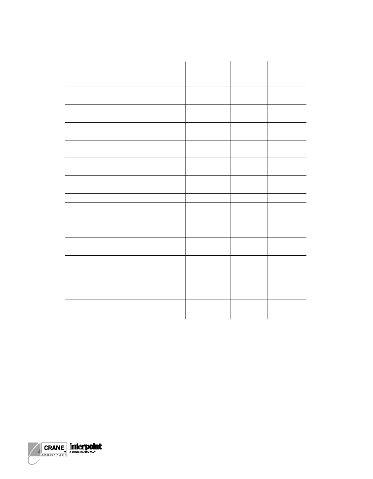
SINGLE OUTPUT MODELS
SMTR283R3S
SMTR2805S
SMTR2812S
SMTR2815S
PARAMETER
CONDITION
MIN
TYP
MAX
MIN TYP
MAX
MIN
TYP
MAX
MIN
TYP
MAX
UNITS
OUTPUT VOLTAGE
3.27
3.30
3.33
4.95
5.00
5.05 11.88 12.00 12.12 14.85 15.00 15.15
VDC
OUTPUT CURRENT
1
V
IN
= 16 to 40 VDC
0
5.45
0
--
5.0
0
--
2.5
0
--
2.0
A
OUTPUT POWER
1
V
IN
= 16 to 40 VDC
0
--
18
0
--
25
0
--
30
0
--
30
W
OUTPUT RIPPLE
10 kHz 2 MHz
--
15
40
--
35
40
--
25
40
--
25
40
mV p-p
VOLTAGE
Tc = 55°C TO +125°C
--
--
50
--
50
90
--
40
90
--
40
90
LINE REGULATION
2
Vin = 16 to 40 VDC
Tc = 55°C TO +125°C
--
--
20
--
15
50
--
15
50
--
15
50
mV
LOAD REGULATION
NO LOAD TO FULL
Tc = 55°C TO +125°C
--
--
20
--
15
50
--
15
50
--
15
50
mV
INPUT VOLTAGE
1
CONTINUOUS
16
28
40
16
28
40
16
28
40
16
28
40
VDC
NO LOAD TO FULL
TRANSIENT 50 ms
--
--
50
--
--
50
--
--
50
--
--
50
V
INPUT CURRENT
1
NO LOAD
--
30
75
--
35
75
--
35
75
--
35
75
mA
FULL LOAD
--
0.94
--
--
1.15
--
--
1.30
--
--
1.25
--
A
INHIBITED
--
7
8
--
3
8
--
3
8
--
3
8
mA
INPUT RIPPLE
10 kHz 10 MHz
CURRENT
Tc = 55°C TO +125°C
--
25
50
--
20
50
--
20
50
--
20
50
mA p-p
EFFICIENCY
74
76
--
74
78
--
78
83
--
79
84
--
%
LOAD FAULT
3
SHORT CIRCUIT
POWER DISSIPATION
--
--
10
--
--
10
--
--
10
--
--
10
W
RECOVERY
1, 4
--
1.4
6
--
1.4
5
--
1.4
5
--
1.4
5
ms
STEP LOAD RESP.
50% 100% 50%
TRANSIENT
--
±125 ±250
--
±200 ±300
--
±250 ±400
--
±350 ±500
mV pk
RECOVERY
4
--
--
200
--
60
200
--
60
200
--
60
200
µs
STEP LINE RESP.
16 40 16 VDC
TRANSIENT
5
--
--
±300
--
±200 ±300
--
±400 ±500
--
±500 ±600
mV pk
RECOVERY
4
--
--
300
--
--
300
--
--
300
--
--
300
µs
START-UP
1
DELAY
--
1.4
5
--
1.4
5
--
1.4
5
--
1.4
5
ms
OVERSHOOT
FULL LOAD
--
0
50
--
0
50
--
0
120
--
0
150
mV pk
NO LOAD
--
33
150
--
50
250
--
120
600
--
150
750
DUAL OUTPUT MODELS
SMTR2805D
SMTR2812D
SMTR2815D
PARAMETER
CONDITIONS
MIN TYP
MAX
MIN
TYP
MAX
MIN
TYP
MAX
UNITS
OUTPUT VOLTAGE
+V
OUT
4.95
5.00
5.05
11.88
12.00
12.12 14.85
15.00
15.15
VDC
V
OUT
4.92
5.00
5.08
11.82
12.00
12.18
14.77
15.00
15.23
OUTPUT CURRENT
1, 2
V
IN
= 16 TO 40 VDC
0
2.5
4.5
0
1.25
2.25
0
1.0
1.8
A
OUTPUT POWER
1, 2
V
IN
= 16 TO 40 VDC
0
--
25
0
--
30
0
--
30
W
OUTPUT RIPPLE
10 kHz - 2 MHz
--
20
50
--
30
80
--
25
80
mV p-p
VOLTAGE +/ V
OUT
Tc = 55°C TO +125°C
--
40
80
--
40
120
--
40
120
LINE REGULATION
3
Tc = 55°C
+V
OUT
--
10
50
--
10
50
--
10
50
mV
V
IN
= 16 TO 40 VDC
TO +125°C
V
OUT
--
50
100
--
50
150
--
50
180
LOAD REGULATION
Tc = 55°C
+V
OUT
--
5
50
--
15
50
--
15
50
mV
NO LOAD TO FULL
TO +125°C
V
OUT
--
25
100
--
30
180
--
30
180
CROSS REGULATION
SEE NOTE 4
--
7
12
--
4
8.3
--
3
8
%
EFFECT ON V
OUT
SEE NOTE 5
--
4
6
--
4
6
--
4
6
INPUT VOLTAGE
1
CONTINUOUS
16
28
40
16
28
40
16
28
40
VDC
NO LOAD TO FULL
TRANSIENT 50 ms
0
--
50
0
--
50
0
--
50
V
INPUT CURRENT
NO LOAD
--
35
75
--
50
75
--
50
75
mA
FULL LOAD
--
1.10
--
--
1.34
--
--
1.29
--
A
INHIBITED
--
3
8
--
3
8
--
3
8
mA
INPUT RIPPLE
CURRENT
1
10 kHz - 10 MHz
--
15
50
--
20
50
--
20
50
mA p-p
EFFICIENCY
74
76
--
77
80
--
78
81
--
%
LOAD FAULT
6
POWER DISSIPATION
SHORT CIRCUIT
1
--
--
10
--
--
10
--
--
10
W
RECOVERY
--
1.4
5.0
--
1.4
5.0
--
1.4
5.0
ms
STEP LOAD
50 100 50% BALANCED
RESPONSE ± V
OUT
TRANSIENT
--
±200
±300
--
±150
±300
--
±200
±400
mV pk
RECOVERY
7
--
100
200
--
100
200
--
100
200
µs
STEP LINE
16 40 16 V
IN
RESPONSE ± V
OUT
TRANSIENT
8
--
±200
±400
--
±200
±400
--
±400
±500
mV pk
RECOVERY
7
--
--
300
--
--
300
--
--
300
µs
STARTUP
1
DELAY
--
1.4
5
--
1.4
5
--
1.4
5
ms
OVERSHOOT
FULL LOAD
--
0
180
--
0
120
--
0
150
mV pk
NO LOAD
--
50
250
--
120
600
--
150
750
3
SMTR SERIES
30 WATT
DC/DC C
ONVERTERS
Notes
1. Tc = 55°C to +125°C.
2. Up to 90% of the total output current/power is available from either output
providing the positive output is carrying at least 10% of the total output
power.
3. Operation is limited below 16 V (see Figure 21).
4. Effect on the negative output under the following conditions:
+P
out
20% to 80%; P
out
80% to 20%
5. Effect on the negative output under the following conditions:
+P
out
50%; P
out
10% to 50%
6. Indefinite short circuit protection not guaranteed above 125°C case.
7. Recovery time is measured from application of the transient to point at which
Vout is within 1% of final value.
8. Transition time
10 µs.
Electrical Characteristics: 25°C Tc, 28 VDC Vin, 100% load, radiation level O, unless otherwise specified.

TRIM AND REMOTE SENSE (AVAILABLE ON SINGLE OUTPUT MODELS ONLY)
4
SMTR SERIES
30 WATT
DC/DC C
ONVERTERS
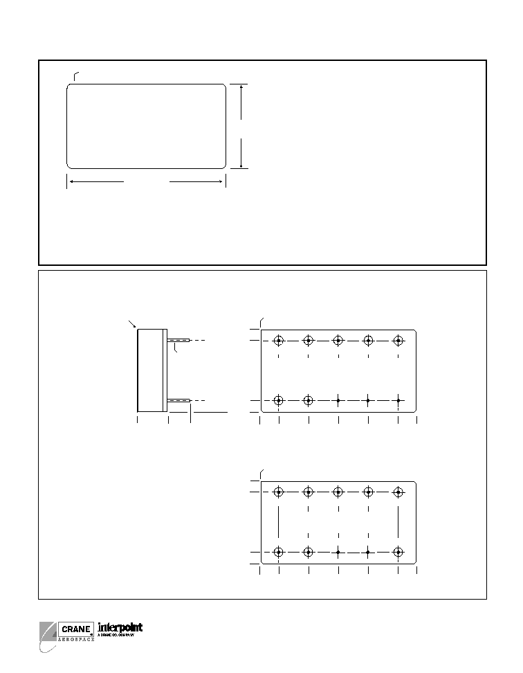
PIN OUT
BOTTOM VIEW
SMTR SINGLE
FLANGED AND NON-FLANGED
Dot on top of cover indicates pin one.
Dotted line outlines flanged package option.
6
10
7
8
9
1
2
3
4
5
F
IGURE
3: P
IN
O
UT
S
INGLE
O
UTPUT
M
ODELS
RL
OUTPUT
COMMON
REMOTE SENSE CONNECTION
2 Make connections at load.
SMTR SINGLE OUTPUT CONVERTER
4
3
5
10
1
+VIN
INPUT
COMMON
6
SENSE
RETURN
SENSE
POSITIVE
OUTPUT
2
2
EXTERNAL TRIM CONNECTION
1 Make connections at converter.
RL
OUTPUT
COMMON
SMTR SINGLE OUTPUT CONVERTER
4
3
5
10
1
+VIN
INPUT
COMMON
6
SENSE
RETURN
SENSE
POSITIVE
OUTPUT
1
RT
1
Pin
Single Output
Dual Output
1
Positive Input
Positive Input
2
Inhibit
Inhibit
3
Sense Return
Positive Output
4
Output Common
Output Common
5
Positive Output
Negative Output
6
Positive Sense
Case Ground
7
Case Ground
Case Ground
8
Case Ground
Case Ground
9
Sync
Sync
10
Input Common
Input Common
BOTTOM VIEW
SMTR DUAL
FLANGED AND NON-FLANGED
Dot on top of cover indicates pin one.
6
10
7
8
9
1
2
3
4
5
Dotted line outlines flanged package option.
F
IGURE
4: P
IN
O
UT
D
UAL
O
UTPUT
M
ODELS
See Figures 22 and 23 and for dimensions.
See Figures 24 and 25 for dimensions.
F
IGURE
2: R
EMOTE
S
ENSE2, 3
F
IGURE
1: T
RIM
C
ONNECTION1, 2, 3
Notes for Remote Sense and Trim
1. When trimming output voltage and/or remote sensing, the total output
voltage increase must be less than 0.6 volts at the converters pins to
maintain specified performance.
2. If neither voltage trim nor remote sense will be used, connect pin 3 to
pin 4 and pin 5 to pin 6 or the output voltage will increase by 1.2 volts.
3. CAUTION: The converter will be permanently damaged if the positive
remote sense (pin 6) is shorted to ground. Damage may also result if
the output common or positive output is disconnected from the load with
the remote sense leads connected to the load.
Trim Formulas
Vout = desired output voltage; Rt = trim resistor
3.3V: Rt = 1300 * Vout 4304
1.2475
5V:
Rt = 1300 * Vout 6512
1.2475
12V: Rt = 1300 * Vout 15631
1.2475
15V: Rt = 1300 * Vout 19498
1.2475

5
SMTR SERIES
30 WATT
DC/DC C
ONVERTERS
Typical Performance Curves: 25°C Tc, 28 VDC Vin, 100% load, free run, unless otherwise specified.
F
IGURE
8
F
IGURE
10
OUTPUT POWER (Watts)
SMTR2812D EFFICIENCY
EFFICIENCY (%)
60
85
80
75
70
65
5
10
15
20
16V
40V
28V
0
10
20
30
40
50
60
70
80
90
100
0.1
1
10
100
FREQUENCY (kHz)
AUDIO REJECTION, SMTR SERIES
ATTENUATION (dB)
OUTPUT POWER (Watts)
SMTR2805S EFFICIENCY
EFFICIENCY (%
)
60
85
80
75
70
65
5
10
15
20
25
16V
40V
28V
F
IGURE
5
OUTPUT POWER (Watts)
SMTR2812S EFFICIENCY
EFFICIENCY (%)
60
85
80
75
70
65
5
16V
28V
40V
10
15
20
F
IGURE
6
OUTPUT POWER (Watts)
SMTR2815D EFFICIENCY
EFFICIENCY (%)
65
90
85
80
75
70
5
10
15
20
40V
28V
16V
F
IGURE
9
F
IGURE
7
OUTPUT POWER (Watts)
SMTR2815S EFFICIENCY
EFFICIENCY (%)
62
87
82
77
72
67
5
16V
28V
40V
10
15
20
25
MODEL NUMBERING KEY
SMD NUMBERS
SMTR 28 05 S F / K R
Base Model
Input Voltage
Output Voltage
Screening
Number of Outputs
(S = single, D = dual)
Radiation Level
Case Option
(Non-flanged case has no designator
in this position)
S
TANDARD
M
ICROCIRCUIT
D
RAWING
(SMD)
5962-0150102HXC
5962-9306802HXC
5962-9306902HXC
5962-9307002HXC
IN PROCESS
IN PROCESS
IN PROCESS
MTR S
ERIES
S
IMILAR
P
ART
SMTR283R3S/HO
SMTR2805S/HO
SMTR2812S/HO
SMTR2815S/HO
SMTR2805D/HO
SMTR2812D/HO
SMTR2815D/HO
To indicate the flanged case option change the "X" to "Z" In the
SMD number. The SMD number shown is for Class H
screening, non-flanged, and no Radiation Hardness Assurance
(RHA) level. See the SMD for the numbers for other screening
and radiation levels. For exact specifications for an SMD
product, refer to the SMD drawing. Call your Interpoint repre-
sentative for status on the SMTR SMD releases which are "in
process." SMDs can be downloaded from
http://www.dscc.dla.mil/programs/smcr

6
SMTR SERIES
30 WATT
DC/DC C
ONVERTERS
DC/DC C
ONVERTERS
Typical Performance Curves: 25°C Tc, 28 VDC Vin, 100% load, free run, unless otherwise specified.
F
IGURE
20
OUTPUT LOAD (%)
COND. B: 50% LOAD +V, 50% to 10% V
COND. A: 50% LOAD V, 50% to 10% +V
CROSS REGULATION
V
O
UT
VOLTAGE C
HANGE (%
)
8
0
8
10
20
30
40
50
7
6
5
4
3
2
1
1
2
3
4
5
6
7
COND A
COND B
2812D
2812D
2815D
2805D
2805D
50
µs/div
10% 100%
SMTR2815D +VOUT STEP LOAD RESPONSE
100mV/div
3W to 15W
15W to 3W
F
IGURE
17
200
µs/div
SMTR2815D TURN-ON INTO NO LOAD
5V/div
20V/div
VIN
+VOUT
VOUT
F
IGURE
18
OUTPUT POWER (Watts)
1% DROP
SMTR SINGLES AND DUALS
LOW LINE DROPOUT
INPUT VOLTAGE (Volts)
13.0
13.5
14.0
14.5
15.0
15.5
16.0
9
12
15
18
21
24
27
30
F
IGURE
21
F
IGURE
19
3
27
6
24
9
21
12
18
15
15
18
12
21
9
24
6
27
3
30
0
+POUT
POUT
0
30
OUTPUT LOAD (Watts)
10% to 90% LOAD +V
90% to 10% LOAD V
CROSS REGULATION
V
O
UT
VOLTAGE CHANGE (%)
10
9
8
7
6
5
4
3
2
1
0
-1
-2
-3
-4
-5
-6
-7
-8
-9
-10
2812D
2815D
2815D
2812D
2805D
2805D
F
IGURE
14
F
IGURE
16
1V/div
20V/div
500
µs / div
SMTR2805S TURN-ON INTO NO LOAD
VIN
VOUT
50
µs/div
25% 50%
SMTR2815D +VOUT STEP LOAD RESPONSE
100mV/div
POUT=15W
7.5W to 15W
15W to 7.5W
50
µs/div
16 TO 40V
SMTR2805S STEP LINE RESPONSE
20mV/div
20V/div
VIN
VOUT
F
IGURE
11
50
µs/div
50% 100%
SMTR2805S STEP LOAD RESPONSE
100mV/div
25W to 12.5W
12.5W to 25W
F
IGURE
12
50
µs/div
16 TO 40
SMTR2815D STEP LINE RESPONSE
20mV/div
20V/div
VIN
+VOUT
VOUT
F
IGURE
15
F
IGURE
13
50
µs/div
10% 100%
SMTR2805S STEP LOAD RESPONSE
200mV/div
25W to 2.5W
2.5W to 25W
7
SMTR SERIES
30 WATT
DC/DC C
ONVERTERS
CASE H
BOTTOM VIEW
See Figure 23 for pin configurations.
2.125 max
(53.98)
1.125 max
(28.58)
Materials
Header Cold Rolled Steel/Nickel/Gold
case H2
Cold Rolled Steel/Nickel/Tin
case H4
Cover Kovar/Nickel
case H2
Cold Rolled Steel/Nickel/Tin
case H4
Pins #52
alloy
ceramic seal
case H1
compression glass seal
case H4
Case dimensions in inches (mm)
Tolerance
±0.005 (0.13) for three decimal places
±0.01 (0.3) for two decimal places
unless otherwise specified
CAUTION
Heat from reflow or wave soldering may damage
the device. Solder pins individually with heat
application not exceeding 300
°C for 10 seconds
per pin.
Dot on top of case indicates pin one
F
IGURE
22: C
ASE
H M
AXIMUM
D
IMENSIONS
0.155 (3.94)
0.955 (24.26)
0.155 (3.94)
0.955 (24.26)
6
10
7
8
9
Platform
Seam Seal
0.000
0.040 dia
(1.02)
0.000
0.000
0.400 max.
(10.16)
0.25 (6.4)
0.245
(6.22)
1.845
(46.86)
2.090
(53.01)
1.110 (28.19)
1
2
6
10
SMTR Series Single
SMTR Series Dual
BOTTOM VIEW CASE H2
3
4
5
7
8
9
0.000
0.000
0.245
(6.22)
1.845
(46.86)
2.090
(53.01)
1.110 (28.19)
1
2
3
4
5
0.645
(16.38)
1.045
(26.54)
1.445
(36.70)
0.645
(16.38)
1.045
(26.54)
1.445
(36.70)
Squared corner and dot on top
of case indicate pin one.
Squared corner and dot on top
of case indicate pin one.
SMTR Series Single
SMTR Series Dual
F
IGURE
23: C
ASE
H2
Note: Although every effort has been made to render the case drawings at actual size, variations in the printing process may cause some distortion. Please refer
to the numerical dimensions for accuracy.

8
SMTR SERIES
30 WATT
DC/DC C
ONVERTERS
Materials
Header Case K3
Cold Rolled Steel/Nickel/Gold
Case K8
Cold Rolled Steel/Nickel/Tin
Cover Case
K3
Kovar/Nickel
Case K8
Cold Rolled Steel/Nickel/Tin
Pins
#52 alloy (all cases)
Case K3
ceramic seal
Case K8
compression glass seal
Case dimensions in inches (mm)
Tolerance
±0.005 (0.13) for three decimal places
±0.01 (0.2) for two decimal places
unless otherwise specified
CASE K
BOTTOM VIEW
See Figures 40 and 41
for pin configuration
CAUTION
Heat from reflow or wave soldering may damage
the device. Solder pins individually with heat
application not exceeding 300
°C for 10 seconds
per pin.
Flange Thickness:
Case K3 0.060 (1.52)
Case K5 0.067 +0.005/-0.007 (1.70 +0.13/-0.8)
1.125 max
(28.58)
2.910 max
(73.91)
Dot on top of case indicates pin one
F
IGURE
24: C
ASE
K M
AXIMUM
D
IMENSIONS

9
SMTR SERIES
30 WATT
DC/DC C
ONVERTERS
0.155 (3.94)
0.955 (24.26)
6
10
7
8
9
0.000
0.400 max.
(10.16)
0.25
±
0.03
(6.4
±
0.8)
0.040 dia
(1.02)
0.000
0.400 max.
(10.16)
0.25
±
0.03
(6.4
±
0.8)
0.040 dia
(1.02)
0.155 (3.94)
0.955 (24.26)
Platform Header
Seam Seal
Platform Header
Seam Seal
0.000
0.000
0.245
(6.22)
0.230
(5.84)
1.845
(46.86)
2.320
(58.93)
0.230
(5.84)
2.320
(58.93)
1.110 (28.19)
1
2
6
10
Flanged cases: Designator "F" required in Case Option position of model number.
SMTR Series Single
SMTR Series Dual
BOTTOM VIEW CASE K3
3
4
5
7
8
9
0.000
0.245
(6.22)
1.845
(46.86)
1
2
3
4
5
0.645
(16.38)
1.045
(26.54)
1.445
(36.70)
0.645
(16.38)
1.045
(26.54)
1.445
(36.70)
0.555 (14.1)
0.000
1.110 (28.19)
0.555 (14.1)
Dot on top of case indicates pin one
Dot on top of case indicates pin one
SMTR Series Single
SMTR Series Dual
0.162 dia
(4.11)
0.162 dia
(4.11)
F
IGURE
25: C
ASE
K3
10
SMTR SERIES
30 WATT
DC/DC C
ONVERTERS
Definitions
Element Evaluation: Component testing/screening per MIL-STD-883 as determined by MIL-PRF-38534
SEM: Scanning Electron Microscopy
SLAMTM: Scanning Laser Acoustic Microscopy
C-SAM: C - Mode Scanning Acoustic Microscopy
T
ABLE
1: E
LEMENT
E
VALUATION
E
LEMENT
E
VALUATION
S
PACE
P
ROTOTYPE
C
LASS
C
LASS
T
EST
P
ERFORMED
(O)
H
K
(
COMPONENT LEVEL
)
M/S
P
M/S
P
M/S
P
Element Electrical
yes
no
yes
yes
yes
yes
Element Visual
no
no
yes
yes
yes
yes
Internal Visual
no
no
yes
no
yes
no
Temperature Cycling
no
no
no
no
yes
yes
Constant Acceleration
no
no
no
no
yes
yes
Interim Electrical
no
no
no
no
yes
no
Burn-in
no
no
no
no
yes
no
Post Burn-in Electrical
no
no
no
no
yes
no
Steady State Life
no
no
no
no
yes
no
Voltage Conditioning /Aging
no
no
no
no
no
yes
Visual Inspection
no
no
no
no
no
yes
Final Electrical
no
no
yes
yes
yes
yes
Wire Bond Evaluation
no
no
yes
yes
yes
yes
SEM
no
no
no
no
yes
no
SLAMTM/C-SAM:
Input capacitors only
no
no
no
yes
no
yes
(Add'l test, not req. by H or K)
Notes
M/S Active components (Microcircuit and Semiconductor Die)
P
Passive components
11
SMTR SERIES
30 WATT
DC/DC C
ONVERTERS
T
ABLE
2: P
RODUCT
E
NVIRONMENTAL
S
CREENING
E
NVIRONMENTAL
S
CREENING
S
PACE
T
EST
P
ERFORMED
P
ROTOTYPE
C
LASS
C
LASS
(
END ITEM LEVEL
)
(O)
H
K
Non-destruct bond pull
Method 2023
no
no
yes
Pre-cap inspection
Method 2017, 2032
yes
yes
yes
Temperature cycle
Method 1010, Cond. C
yes
yes
yes
Constant acceleration
Method 2001, 3000 g
yes
yes
yes
PIND Test
Method 2020, Cond. B
no
yes
yes
Radiography
Method 2012
no
no
yes
Pre burn-in test
yes
yes
yes
Burn-in, Method 1015, 125°C
96 hours
yes
no
no
160 hours
no
yes
no
2 x 160 hour (includes mid BI test)
no
no
yes
Final electrical test
MIL-PRF-38534, Group A
yes
yes
yes
Hermeticity test
Fine Leak,
Method 1014, Cond. A
yes
yes
yes
Gross Leak,
Method 1014, Cond. C
yes
yes
yes
Final visual inspection
Method 2009
yes
yes
yes
Test methods are referenced to MIL-STD-883 as determined by MIL-PRF-38534.

12
SMTR SERIES
30 WATT
DC/DC C
ONVERTERS
11978-DTS Rev D. This revision supercedes all previous releases.
All technical information is believed to be accurate, but no responsibility is
assumed for errors or omissions. Interpoint reserves the right to make changes in
products or specifications without notice. SMTR Series is a trademark of Interpoint.
Copyright © 1994 - 2003 Interpoint. All rights reserved.
T
ABLE
3: R
ADIATION
H
ARDNESS
L
EVELS
Contact Information:
Interpoint Headquarters USA
Phone:
1-800-822-8782
+425-882-3100
Email:
power@intp.com
www.interpoint.com
Interpoint UK
Phone:
+44-1252-872266
Email:
poweruk@intp.com
Interpoint France
Phone:
+33-134285455
Email:
powerfr@intp.com
PRODUCT LEVEL AVAILABILITY
ENVIRONMENTAL SCREENING LEVELS
SPACE
PROTOTYPE CLASS CLASS
RADIATION HARDNESS LEVELS
(O)
H
K
O: Standard, no radiation guarantee
For system evaluation, electrically
OO
HO
Not
and mechanically comparable to
available
H and K level.
R: Radiation hardened Tested lots
Not
Up to 100 k Rads (Si) total dose
available
HR
KR
SEU guarantee up to 40 MeV
T
ABLE
4:
R
EPORTS
: A
VAILABLE FOR CUSTOMER REVIEW AT
I
NTERPOINT
1. Radiation Susceptibility Analysis
2. Electrical/Thermal Stress Analysis and Derating Report
3. MTBF Report
4. FMEA Report
HO option: Reports 2, 3, and 4 are included with purchase.
OO option: Select reports available as separate purchases.
R is referenced to MIL-PRF-38534, appendix G, Radiation Hardness Assurance
(RHA) levels.