
MODELS
VDC O
UTPUT
33
SINGLE
3.3
5
12
15
DUAL
±5
±12
±15
DC/DC C
ONVERTERS
28 V
OLT
I
NPUT
SMHF SERIES
SINGLE AND DUAL
15 WATT
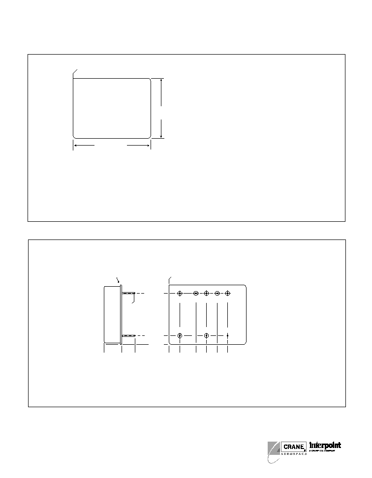
Size (max.): Non flanged 1.460 x 1.130 x 0.330 (37.08 x 28.70 x 8.38 mm)
Flanged 2.005 x 1.130 x 0.330 (50.93 x 28.70 x 8.38 mm)
See Figures 21 through 24 for dimensions.
Weight:
30 grams maximum.
Screening: Standard, Class H, or Class K (MIL-PRF-38534)
Radiation hardness levels O, L, and R
DESCRIPTION
The SMHF SeriesTM of 28 V DC/DC converters offers a wide input
voltage range of 16 to 40 volts and up to 15 watts of output power.
The units are capable of withstanding short term transients up to 50
volts. The package is a hermetically sealed, seam-welded metal
case. Flanged and non-flanged models are available.
S
CREENING AND
R
EPORTS
SMHF converters offer three screening options (Standard, Class H,
or Class K) and three levels of radiation hardness (O, L, and R). See
Tables 1, 2, and 3 for more information. Detailed reports on product
performance are also available and are listed in Table 4.
C
ONVERTER
D
ESIGN
The SMHF converters are switching regulators that use a quasi-
square wave, single-ended forward converter design with a constant
switching frequency of 550 kHz. Isolation between input and output
circuits is provided with a transformer in the forward path and a
temperature compensated opto-coupler in the feedback control
loop. The opto-coupler is radiation hardened and is especially
selected for space applications.
For the SMHF dual output models, cross regulation is maintained by
tightly coupled output magnetics. Up to 70% of the total output
power is available from either output, providing the opposite output
is simultaneously carrying 30% of the total output power. Predictable
current limit is accomplished by directly monitoring the output load
current and providing a constant current output above the overload
point.
H
IGHER
P
OWER
D
ENSITY
The SMHF Series offers a new standard of performance for small
size and high power density. At just 0.33 inch high and a total foot-
print of 1.7 in
2
, this low profile package offers a total power density
of up to 30 watts per cubic inch.
L
OW
N
OISE
, H
IGH
A
UDIO
R
EJECTION
The SMHF converters' feed-forward compensation system provides
excellent dynamic response and noise rejection. Audio rejection is
typically 50 dB. Typical output voltage response for a 50% to 100%
step load transient is as low as 1.3% with a 150 msec recovery time.
Input ripple current is typically 35 mA p-p with output ripple voltage
typically 30 mV p-p .
I
NHIBIT
F
UNCTION
SMHF converters provide an inhibit terminal that can be used to
disable internal switching, resulting in no output and very low quies-
cent input current. The converter is inhibited when a TTL compatible
low (
0.8 output disabled) is applied to the inhibit pin. The unit is
enabled when the pin, which is internally connected to a pull-up
resistor, is left unconnected or is connected to an open-collector
gate. The open circuit output voltage associated with the inhibit pin
is 8.5 to 12 VDC. In the inhibit mode, a maximum of 12 mA must be
sunk from the inhibit pin at 28 VDC input.
S
YNCHRONIZATION
A synchronization feature is included with the SMHF Series that
allows the user to match the switching frequency of the converter to
the frequency of the system clock. An external synchronization
feature is included that allows the user to adjust the nominally
550kHz operating frequency to any frequency within the range of
500 kHz to 600 kHz. This is initiated by applying a TTL compatible
input of the desired frequency to pin 5.
S
HORT
C
IRCUIT
P
ROTECTION
SMHF Series converters provide short circuit protection by
restricting the output current to approximately 115% of the full load
output current. The output current is sensed in the secondary stage
to provide highly predictable and accurate current limiting, and to
eliminate foldback characteristics.
U
NDERVOLTAGE
L
OCKOUT
Undervoltage lockout prevents the units from operating below
approximately 14 VDC input voltage to keep system current levels
smooth, especially during initialization or re-start operations.
F
EATURES
· Fully qualified to Class H or K
· Radiation hardened
· 55° to +125°C operation
· 16 to 40 VDC input
· Fully Isolated
· Red hard optocoupler feedback
· Fixed frequency, 550 kHz typical
· Topology Single Ended Forward
· Transient protection 50 V/120 ms
· Inhibit function
· Sync function
· Indefinite short circuit protection
· Undervoltage lockout
· Up to 84% efficiency

RECOMMENDED OPERATING CONDITIONS
TYPICAL CHARACTERISTICS
SYNC AND INHIBIT
ABSOLUTE MAXIMUM RATINGS
Input Voltage
· 16 to 40 VDC
Power Dissipation (Pd)
· 8 W
Output Power
· 12 to 15 watts depending on model
Lead Soldering Temperature (10 sec per lead)
· 300°C
Storage Temperature Range (Case)
· 65°C to +150°C
34
DC/DC C
ONVERTERS
Output Voltage Temperature Coefficient
· 100 ppm /°C typical
· 150 ppm/°C maximum
Input to Output Capacitance
· 60 pF typical
Undervoltage Lockout
· 12 V input typical
Current Limit
· 115% of full load typical
Isolation
· 100 megohm minimum at 500 V
Audio Rejection
· 50 dB typical
Conversion Frequency (ş55°C to +125°C Tc)
· Free run 550 kHz typical
480 kHz min, 620 kHz max
Inhibit Pin Voltage (unit enabled)
· 8.5 to 12 V
Input Voltage Range
· 16 to 40 VDC continuous
· 0 V for up to 50 msec transient
Case Operating Temperature (Tc)
· 55°C to +125°C full power
· 55°C to +135°C absolute
Derating Output Power/Current (Tc)
· Linearly from 100% at 125°C to 0% at 135°C
SMHF SERIES
SINGLE AND DUAL
15 WATT
SINGLE OUTPUT MODELS
SMHF283R3S
SMHF2805S
SMHF2812S
SMHF2815S
OUTPUT VOLTAGE
Tc = 25°C
3.27
3.3
3.33
4.95
5
5.05 11.88
12
12.12 14.85
15
15.15
VDC
OUTPUT CURRENT
V
IN
= 16 TO 40 VDC
--
--
2.4
--
--
2.4
--
--
1.25
--
--
1.00
A
OUTPUT POWER
V
IN
= 16 TO 40 VDC
0
--
8
0
--
12
0
--
15
0
--
15
W
OUTPUT RIPPLE
10 kHz - 2 MHz
--
60
160
--
30
80
--
60
160
--
60
75
mV p-p
VOLTAGE
Tc = 55°C TO +125°C
--
80
240
--
150
240
--
50
120
--
100
260
LINE REGULATION
V
IN
= 16 TO 40 VDC
--
5
100
--
5
100
--
5
100
--
5
100
mV
LOAD REGULATION
NO LOAD TO FULL
--
20
50
--
20
50
--
20
50
--
20
50
mV
INPUT VOLTAGE
CONTINUOUS
16
28
40
16
28
40
16
28
40
16
28
40
VDC
NO LOAD TO FULL
TRANSIENT 120 ms
0
--
50
0
--
50
0
--
50
0
--
50
V
INPUT CURRENT
NO LOAD
--
25
65
--
25
40
--
25
50
--
25
62
FULL LOAD
--
--
397
--
560
624
--
680
752
--
670
752
mA
INHIBITED
--
5
12
--
5
12
--
5
12
--
5
12
INPUT RIPPLE
10k Hz - 10 MHz
--
45
80
--
35
80
--
35
80
--
35
80
mA p-p
CURRENT
Tc = 55°C TO +125°C
--
--
120
--
--
120
--
--
120
--
--
120
EFFICIENCY
Tc = 25°C
70
73
--
73
75
--
78
79
--
74
80
--
%
LOAD FAULT
1
SHORT CIRCUIT
POWER DISSIPATION
--
5
8
--
3.5
8
--
3.5
8
--
3.5
7
W
RECOVERY
2
--
7.5
30
--
7.5
30
--
7.5
30
--
7.5
30
ms
STEP LOAD
50 %100% 50%
RESPONSE
TRANSIENT
400
150
500
500
150
500
700
150
700
800
200
800
mV pk
RECOVERY
2
--
150
300
--
150
300
--
150
500
--
600
1200
µs
STEP LINE
16 TO 40 TO 16 V
IN
RESPONSE
TRANSIENT
3
800
550
800
800
550
800
800
550
800
800
550
800
mV pk
RECOVERY
2
--
0.8
1.2
--
0.8
1.2
--
0.8
1.2
--
0.8
1.2
µs
START-UP
DELAY
--
10
25
--
10
25
--
10
25
--
10
25
µs
0 TO 28 VIN
OVERSHOOT
4
--
200
300
--
100
600
--
200
1200
--
200
1500
mV pk
Notes
1. Indefinite short circuit protection not guaranteed above 125°C (case)
2. Recovery time is measured from application of the transient
to the point at which Vout is within regulation.
3. Input step transition time >10µs.
4. Input step transition time <100µs.
Sync In (500 to 600 kHz)
· Duty cycle 40% to 60%
· Logic low 0.8 V max
· Logic high 4.5 V min, 5 V max
· Referenced to input common
· If not used, connect to input common
Inhibit TTL Open Collector
· Logic low (output disabled)
Logic low voltage
0.8 V max
Inhibit pin current 4.0 mA max
· Referenced to input common
· Logic high (output enabled)
Open collector or unconnected
Electrical Characteristics: 25°C Tc, 28 VDC Vin, 100% load, radiation level O, unless otherwise specified.

35
DC/DC C
ONVERTERS
SMHF SERIES
SINGLE AND DUAL
15 WATT
DUAL OUTPUT MODELS
SMHF2805D
SMHF2812D
SMHF2815D
PARAMETER
CONDITIONS
MIN
TYP
MAX
MIN
TYP
MAX
MIN
TYP
MAX
UNITS
OUTPUT VOLTAGE
+V
OUT
4.95
5.00
5.05
11.88
12.00
12.12
14.85
15.00
15.15
VDC
V
OUT
4.92
5.00
5.08
11.82
12.00
1218
14.78
15.00
15.23
OUTPUT CURRENT
1
V
IN
= 16 to 40 VDC
--
±1.2
1.68
--
±0.625
0.875
--
±0.500
0.700
A
OUTPUT POWER
1
V
IN
= 16 to 40 VDC
--
--
12
--
--
15
--
--
15
W
OUTPUT RIPPLE
10 kHz - 2 MHz
--
60
160
--
70
175
--
70
175
VOLTAGE ±V
OUT
Tc = 55°C to +125°C
--
100
240
--
100
275
--
100
275
mV p-p
LINE REGULATION
BALANCED +V
OUT
--
5
50
--
5
50
--
5
50
mV
Vin = 16 to 40 VDC
LOAD
V
OUT
--
--
100
--
--
100
--
--
100
LOAD REGULATION
BALANCED +V
OUT
--
20
50
--
20
50
--
20
50
mV
LOAD
V
OUT
--
--
150
--
--
150
--
--
150
CROSS REGULATION
2
NEGATIVE V
OUT
--
6
7.5
--
3
6
--
3
6
%
INPUT VOLTAGE
CONTINUOUS
16
28
40
16
28
40
16
28
40
VDC
NO LOAD TO FULL
TRANSIENT 50 msec
--
--
50
--
--
50
--
--
50
V
INPUT CURRENT
NO LOAD
--
20
50
--
25
50
--
25
50
FULL LOAD
--
540
600
--
645
754
--
638
754
mA
INHIBITED
--
6
12
--
5
12
--
5
12
INPUT RIPPLE
10 kHz - 10 MHz
--
30
80
--
40
80
--
40
80
CURRENT
Tc = 55°C to +125°C
--
60
120
--
55
120
--
55
120
mA p-p
EFFICIENCY
75
77
--
74
81
--
74
82
--
%
LOAD FAULT
SHORT CIRCUIT
3
POWER DISSIPATION
--
3
8
--
3
6
--
3
6
W
RECOVERY
4
--
7.5
30
--
7.5
50
--
7.5
50
ms
STEP LOAD RESP.
5
50% 100% 50%
BALANCED LOADS
TRANSIENT
+V
OUT
600
200
600
600
300
600
600
300
600
mV pk
V
OUT
600
150
600
600
100
500
600
100
600
RECOVERY
4
--
150
500
--
200
500
--
200
600
µs
STEP LINE RESP.
16 40 40 VDC
± V
OUT
TRANSIENT
6
800
600
800
750
550
750
750
550
750
mV pk
RECOVERY
4
--
0.8
1.2
--
0.8
1.2
--
0.8
1.2
ms
START-UP
DELAY
--
12
30
--
12
25
--
12
25
ms
OVERSHOOT
7
0
100
500
0
200
500
0
200
500
mV pk
Notes
1. Up to 70% of the total output power is available from either output providing
the opposite output is simultaneously carrying 30% of the total output
power. Each output must carry a minimum of 30% of the total output
power in order to maintain regulation on the negative outputs.
2. Effect on Vout for the following conditions, percentages are of total power:
+Po = 50% to 10% and Po = 50%
+Po = 50% and Po = 50% to 10%
3. Indefinite short circuit protection not guaranteed above 125°C (case)
4. Recovery time is measured from application of the transient to point at
which Vout is within regulation.
5. Response of either output with the opposite output held at half of the total
output power.
6. Input step transition time >10µs.
7. Input step transition time <100µs.
Electrical Characteristics: 25°C Tc, 28 VDC Vin, 100% load, radiation level O, unless otherwise specified.

36
DC/DC C
ONVERTERS
SMHF SERIES
SINGLE AND DUAL
15 WATT
PWM
Controller
I
D
I
C
Limit
Ref.
Output
Common
Positive
Output
Positive
Input
Inhibit
Input
Common
5
µH
2
µF
FET
Driver
BLOCK DIAGRAM
F
IGURE
1: SMHF S
INGLE
O
UTPUT

DC/DC C
ONVERTERS
SMHF SERIES
SINGLE AND DUAL
15 WATT
PIN OUT
SMHF 28 05 S F / K R
Base Model
Input Voltage
Output Voltage
Screening
Number of Outputs
(S = single, D = dual)
Radiation Level
Case Option
(Non-flanged case has no designator
in this position)
MODEL NUMBERING KEY
Pin
Single Output
Dual Output
1
Inhibit
Inhibit
2
No connection
Positive Output
3
Output Common
Output Common
4
Positive Output
Negative Output
5
1
Sync Sync
6
Case Ground
Case Ground
7
Input Common
Input Common
8
Positive Input
Positive Input
1. If Sync is not used, pin 5 should be connected to input common.
F
IGURE
2: P
IN
O
UT
BOTTOM VIEW
SMHF SINGLE AND DUAL
NON-FLANGED OR FLANGED
Dot on top of cover
indicates pin one.
Dotted line outlines flanged package option.
1
2
3
4
5
8
7
6
See Figures 21 through 24 for dimensions.
SMD NUMBERS
S
TANDARD
M
ICROCIRCUIT
D
RAWING
(SMD)
5962-9213902HXC
IN PROCESS
5962-9160102HXC
5962-9555902HXC
5962-9214402HXC
5962-9161402HXC
SMHF
S
IMILAR
P
ART
SMHF2805S/HO
SMHF2812S/HO
SMHF2815S/HO
SMHF2805D/HO
SMHF2812D/HO
SMHF2815D/HP
To indicate the flanged case option change the "X" to "Z" In the
SMD number. The SMD number shown is for Class H
screening, non-flanged, and no Radiation Hardness Assurance
(RHA) level. See the SMD for the numbers for other screening
and radiation levels. For exact specifications for an SMD
product, refer to the SMD drawing. Call your Interpoint repre-
sentative for status on the SMHF SMD releases which are "in
process." SMDs can be downloaded from
http://www.dscc.dla.mil/programs/smcr
37

DC/DC C
ONVERTERS
SMHF SERIES
SINGLE AND DUAL
15 WATT
Typical Performance Curves: 25°C Tc , 28 VDC Vin, 100% load, free run, unless otherwise specified.
F
IGURE
6
F
IGURE
8
OUTPUT POWER (Watts)
SMHF2805D EFFICIENCY
E
F
F
IC
IE
N
C
Y
(
%
)
40
90
80
70
60
50
2
4
6
8
10
12
40V
28V
16V
OUTPUT POWER (Watts)
SMHF2815D EFFICIENCY
E
F
F
IC
IE
N
C
Y
(
%
)
40
90
80
70
60
50
2
4
6
8
10
12
14
40V
28V
16V
OUTPUT POWER (Watts)
SMHF 2805S EFFICIENCY
E
F
F
IC
IE
N
C
Y
(
%
)
40
90
80
70
60
50
2
4
6
8
10
12
16V
28V
40V
F
IGURE
3
OUTPUT POWER (Watts)
SMHF2812S EFFICIENCY
E
F
F
IC
IE
N
C
Y
(
%
)
40
90
80
70
60
50
2
4
6
8
10
12
14
16V
40V
28V
15
F
IGURE
4
OUTPUT POWER (Watts)
SMHF2812D EFFICIENCY
E
F
F
IC
IE
N
C
Y
(
%
)
40
90
80
70
60
50
2
4
6
8
10
12
14
40V
28V
16V
15
F
IGURE
7
F
IGURE
5
OUTPUT POWER (Watts)
SMHF2815S EFFICIENCY
E
F
F
IC
IE
N
C
Y
(
%
)
40
90
80
70
60
50
2
4
6
8
10
12
14
16V
40V
15
28V
FREQUENCY (kHz)
SMHF SERIES AUDIO REJECTION
A
T
T
E
N
U
A
T
IO
N
(d
B
)
100
0.1
1
10
100
90
80
70
60
50
40
20
10
0
30
F
IGURE
9
1ms/div
16V TO 40V
SMHF2805S STEP LINE RESPONSE
5
0
0
m
V
/d
iv
.
VIN
2
0
V
/d
iv
.
VOUT
F
IGURE
10
F
IGURE
11
50
µs/div
50% 100%
SMHF2805S STEP LOAD RESPONSE
100mV/div.
50% to 100%
100% to 50%
38

DC/DC C
ONVERTERS
SMHF SERIES
SINGLE AND DUAL
15 WATT
Typical Performance Curves: 25°C Tc , 28 VDC Vin, 100% load, free run, unless otherwise specified.
F
IGURE
18
F
IGURE
20
POSITIVE OUTPUT LOAD (% OF TOTAL LOAD)
V
OUT
WITH SHIFT IN LOAD BALANCE
CROSS REGULATION
V
OUT
V
O
L
T
A
G
E
C
H
A
N
G
E
(
%
)
10
100
0
20
40
60
80
5
0
5
10
2812D
2815D
2805D
OUTPUT POWER (Watts)
50 mV DROP
LOW LINE DROPOUT VS. LOAD
IN
P
U
T
V
O
L
T
A
G
E
(
V
o
lts
)
10
11
12
13
14
15
14
15
16
SMHF2812S&D
SMHF2815S&D
SMHF2805S&D
13
12
50
µs/div
50% 100%
SMHF2815D +V
STEP LOAD RESPONSE
100mV/div.
50% to 100%
100% to 50%
PO= 7.5 W
F
IGURE
15
50
µs/div
20% 100%
SMHF+2815D VOUT STEP LOAD RESPONSE
1
0
0
m
V
/d
iv
.
20% to 100%
100% to 20%
PO= 7.5 W
F
IGURE
16
OUTPUT LOAD (%)
COND. A: 50% LOAD +V; 50% to 10% V
COND. B: 50% LOAD V; 50% to 10% +V
SMHF2805D/SMHF2812D/SMHF2815D
CROSS REGULATION
V
O
U
T
V
O
L
T
A
G
E
C
H
A
N
G
E
(%
)
10
0
10
10
20
30
40
50
8
6
4
2
2
4
6
8
2815D
2812D
2812D
COND B
COND A
2805D
2805D
F
IGURE
19
F
IGURE
17
2 ms/div
SMHF2815D TURN-ON INTO FULL LOAD
2
0
V
/d
iv
.
VIN
5
V
/d
iv
.
+VOUT
VOUT
F
IGURE
12
F
IGURE
14
200
µs/div
10% 100%
SMHF2805S STEP LOAD RESPONSE
100mV/div.
10% to 100%
100% to 10%
1 ms/div
16V TO 40V
SMHF2815D STEP LINE RESPONSE
2
0
0
m
V
/d
iv
.
VIN
2
0
V
/d
iv
.
+VOUT
2 ms/div
SMHF2805S TURN-ON INTO FULL LOAD
1V/div.
VIN
20V/div.
VOUT
POUT= 12W
F
IGURE
13
39
40
DC/DC C
ONVERTERS
SMHF SERIES
SINGLE AND DUAL
15 WATT
Note: Although every effort has been made to render the case drawings at actual size, variations in the printing process may cause some distortion. Please refer
to the numerical dimensions for accuracy.
CASE E
BOTTOM VIEW
See Figure 22
for pin configurations.
Squared corner and dot on top
of case indicate pin one.
1.460 max
(37.08)
1.130 max
(28.70)
Materials
Header Cold Rolled Steel/Nickel/Gold
Cover Kovar/Nickel
(SMHF Series
Cold Rolled Steel/Nickel/Gold)
Pins #52
alloy/Gold
compression glass seal
Case dimensions in inches (mm)
Tolerance
±0.005 (0.13) for three decimal places
±0.01 (0.3) for two decimal places
unless otherwise specified
CAUTION
Heat from reflow or wave soldering may damage
the device. Solder pins individually with heat
application not exceeding 300
°C for 10 seconds
per pin.
F
IGURE
21: C
ASE
E M
AXIMUM
D
IMENSIONS
0.000
0.205
(5.21)
0.505
(12.83)
0.705
(17.91)
0.905
(22.99)
1.105
(28.07)
0.330 max
(8.38)
0.000
0.25 (6.35)
0.000
0.160
(4.06)
0.960
(24.38)
1
2
3
4
5
0.030 dia.
(0.76)
8
7
6
SMHF Series Single and Dual
BOTTOM VIEW CASE E1
Projection Weld
Squared corner and dot on top
of case indicate pin one.
F
IGURE
22: C
ASE
E1

41
DC/DC C
ONVERTERS
SMHF SERIES
SINGLE AND DUAL
15 WATT
Materials
Header Cold Rolled Steel/Nickel/Gold
Cover
MHF+ Series and FMH Filter
Kovar/Nickel
SMHF
Cold Rolled Steel/Nickel
Pins
#52 alloy (all cases)
compression glass seal
Case dimensions in inches (mm)
Tolerance
±0.005 (0.13) for three decimal places
±0.01 (0.2) for two decimal places
unless otherwise specified
CASE G
BOTTOM VIEW
Flanged package
See Figure 24
for pin configuration
2.005 max
(50.93)
1.130 max
(28.70)
Squared corner and dot on top
of case indicate pin one.
CAUTION
Heat from reflow or wave soldering may damage
the device. Solder pins individually with heat
application not exceeding 300
°C for 10 seconds
per pin.
Flange Thickness: 0.047 (1.19)
F
IGURE
23: C
ASE
G M
AXIMUM
D
IMENSIONS
1.590 (40.39)
0.128 dia
(3.25)
0.030 dia.
(0.76)
Flanged cases: Designator "F" required in Case Option position of model number
SMHF Series Single and Dual
BOTTOM VIEW CASE G1
0.000
0.205 (5.21)
0.505 (12.83)
0.705 (17.91)
0.905 (22.99)
1.105 (28.07)
0.000
0.160
(4.06)
0.960
(24.38)
1
2
3
4
5
8
7
6
0.140 (3.56)
0.560
(14.22)
0.330 max.
(8.38)
0.000
0.25 (6.35)
Squared corner and dot on top
of case indicate pin one.
Projection Weld
F
IGURE
24: C
ASE
G1

42
DC/DC C
ONVERTERS
SMHF SERIES
SINGLE AND DUAL
15 WATT
Definitions
Element Evaluation: Component testing/screening per MIL-STD-883 as determined by MIL-PRF-38534
SEM: Scanning Electron Microscopy
SLAMTM: Scanning Laser Acoustic Microscopy
C-SAM: C - Mode Scanning Acoustic Microscopy
Notes
M/S Active components (Microcircuit and Semiconductor Die)
P
Passive components
T
ABLE
1: E
LEMENT
E
VALUATION
E
LEMENT
E
VALUATION
S
PACE
P
ROTOTYPE
C
LASS
C
LASS
T
EST
P
ERFORMED
(O)
H
K
(
COMPONENT LEVEL
)
M/S
P
M/S
P
M/S
P
Element Electrical
yes
no
yes
yes
yes
yes
Element Visual
no
no
yes
yes
yes
yes
Internal Visual
no
no
yes
no
yes
no
Temperature Cycling
no
no
no
no
yes
yes
Constant Acceleration
no
no
no
no
yes
yes
Interim Electrical
no
no
no
no
yes
no
Burn-in
no
no
no
no
yes
no
Post Burn-in Electrical
no
no
no
no
yes
no
Steady State Life
no
no
no
no
yes
no
Voltage Conditioning /Aging
no
no
no
no
no
yes
Visual Inspection
no
no
no
no
no
yes
Final Electrical
no
no
yes
yes
yes
yes
Wire Bond Evaluation
no
no
yes
yes
yes
yes
SEM
no
no
no
no
yes
no
SLAMTM/C-SAM:
Input capacitors only
no
no
no
yes
no
yes
(Add'l test, not req. by H or K)

43
DC/DC C
ONVERTERS
T
ABLE
2: P
RODUCT
E
NVIRONMENTAL
S
CREENING
SMHF SERIES
SINGLE AND DUAL
15 WATT
E
NVIRONMENTAL
S
CREENING
S
PACE
T
EST
P
ERFORMED
P
ROTOTYPE
C
LASS
C
LASS
(
END ITEM LEVEL
)
(O)
H
K
Non-destruct bond pull
Method 2023
no
no
yes
Pre-cap inspection
Method 2017, 2032
yes
yes
yes
Temperature cycle
Method 1010, Cond. C
yes
yes
yes
Constant acceleration
Method 2001, 3000 g
yes
yes
yes
PIND Test
Method 2020, Cond. B
no
yes
yes
Radiography
Method 2012
no
no
yes
Pre burn-in test
yes
yes
yes
Burn-in, Method 1015, 125°C
96 hours
yes
no
no
160 hours
no
yes
no
2 x 160 hour (includes mid BI test)
no
no
yes
Final electrical test
MIL-PRF-38534, Group A
yes
yes
yes
Hermeticity test
Fine Leak,
Method 1014, Cond. A
yes
yes
yes
Gross Leak,
Method 1014, Cond. C
yes
yes
yes
Final visual inspection
Method 2009
yes
yes
yes
Test methods are referenced to MIL-STD-883 as determined by MIL-PRF-38534.

44
DC/DC C
ONVERTERS
11921-001-DTS Rev B This revision supercedes all previous releases.
All technical information is believed to be accurate, but no responsibility is assumed
for errors or omissions. Interpoint reserves the right to make changes in products or
specifications without notice. SMHF Series is a trademark of Interpoint. Copyright
© 1997-2000 Interpoint. All rights reserved.
T
ABLE
3: R
ADIATION
H
ARDNESS
L
EVELS
SMHF SERIES
SINGLE AND DUAL
15 WATT
Contact Information:
Interpoint Headquarters USA
Phone:
1-800-822-8782
+425-882-3100
Email:
power@intp.com
www.interpoint.com
Interpoint UK
Phone:
+44-1252-872266
Email:
poweruk@intp.com
Interpoint France
Phone:
+33-134285455
Email:
powerfr@intp.com
PRODUCT LEVEL AVAILABILITY
ENVIRONMENTAL SCREENING LEVELS
SPACE
PROTOTYPE CLASS CLASS
RADIATION HARDNESS LEVELS
(O)
H
K
O: Standard, no radiation guarantee
For system evaluation, electrically
OO
HO
Not
and mechanically comparable to
available
H and K level.
R: Radiation hardened Tested lots
Not
Up to 100 k Rads (Si) total dose
available
HR
KR
SEU guarantee up to 40 MeV
T
ABLE
4:
R
EPORTS
I
NCLUDED WITH PURCHASE OF PRODUCT
HR or KR
1. Radiation Susceptibility Analysis
2. Electrical/Thermal Stress Analysis and Derating Report
3. MTBF Report
4. FMEA Report
HO option: Reports 2, 3, and 4 are included with purchase.
OO option: Select reports available as separate purchases.
R is referenced to MIL-PRF-38534, appendix G, Radiation Hardness Assurance
(RHA) levels.