November 1991
Order Number 271092-005
M80C287
80-BIT CHMOS III NUMERIC PROCESSOR EXTENSION
Military
Y
High Performance 80-Bit Internal
Architecture
Y
Implements ANSI IEEE Standard 754-
1985 for Binary Floating-Point
Arithmetic
Y
Implements Extended M387 Numerics
Coprocessor Instruction Set
Y
Two to Three Times M8087 M80287
Performance at Equivalent Clock Speed
Y
Low Power Consumption
Y
Upward Object-Code Compatible from
M8087 and M80287
Y
Interfaces with M80286 and M80C286
CPUs
Y
Expands CPU's Data Types to Include
32- 64- 80-Bit Floating Point 32- 64-
Bit Integers and 18-Digit BCD Operands
Y
Directly Extends CPU's Instruction Set
to Trigonometric Logarithmic
Exponential and Arithmetic
Instructions for All Data Types
Y
Full-Range Transcendental Operations
for SINE COSINE TANGENT
ARCTANGENT and LOGARITHM
Y
Built-In Exception Handling
Y
Operates in Both Real and Protected
Mode Systems
Y
Eight 80-Bit Numeric Registers Usable
as Individually Addressable General
Registers or as a Register Stack
Y
Available in 40-pin CERDIP
(See Packaging Outlines and Dimensions order
231369)
Y
Military Temperature Range
b
55 C to
a
125 C (T
C
)
The Intel M80C287 is a high-performance numerics processor extension that extends the architecture of the
M80C286 CPU with floating point extended integer and BCD data types A computing system that includes
the M80C287 fully conforms to the IEEE Floating Point Standard Using a numerics oriented architecture the
M80C287 adds over seventy mnemonics to the instruction set of the M80C286 CPU making a complete
solution for high-performance numerics processing The M80C287 is implemented with 1 5 micron high-speed
CHMOS III technology and packaged in a 40-pin CERDIP The M80C287 is upward object-code compatible
from the M80287 and M8087 numerics coprocessors With proper socket design either an M80287 or an
M80C287 can use the same socket
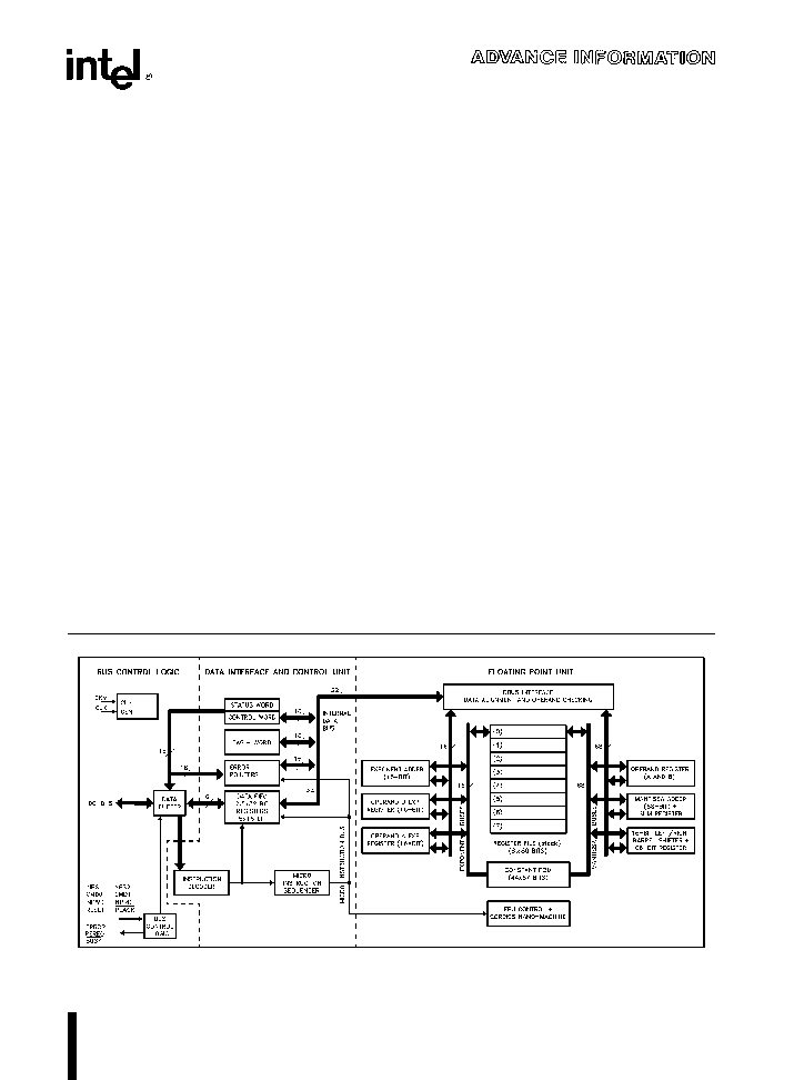
271092 Ł 1
Figure 1 M80C287 Block Diagram
M80C287
M80C287 Data Registers
79
78
64 63
0
R0 Sign
Exponent
Significand
R1
R2
R3
R4
R5
R6
R7
15
0
31
15
0
Control Register
Instruction Pointer
Status Register
Data Pointer
Tag Word
Figure 2 M80C287 Register Set
FUNCTIONAL DESCRIPTION
The M80C287 Numeric Processor Extension (NPX)
provides arithmetic instructions for a variety of nu-
meric data types It also executes numerous built-in
transcendental functions (e g tangent sine cosine
and log functions) The M80C287 effectively ex-
tends the register and instruction set of the CPU for
existing data types and adds several new data types
as well Figure 2 shows the additional registers visi-
ble to programs in a system that includes the
M80C287 Essentially the M80C287 can be treated
as an additional resource or an extension to the
M80C286 CPU The M80C286 CPU together with an
M80C287 NPX can be used as a single unified sys-
tem
The M80C287 has two operating modes After reset
the M80C287 is in the real-address mode It can be
placed into protected mode by executing the
FSETPM instruction It can be switched back to real-
address mode by executing the FRSTPM instruction
(note that this feature is useful only with CPU's that
can also switch back to real-address mode) These
instructions control the format of the administrative
instructions
FLDENV
FSTENV
FRSTOR
and
FSAVE Regardless of operating mode all refer-
ences to memory for numerics data or status infor-
mation are performed by the M80C286 CPU and
therefore obey the memory-management and pro-
tection rules of the M80C286 CPU
In real-address mode a system that includes the
M80C287 is completely upward compatible with
software for the M8086 M8087 and for M80286
M80287 real-address mode
In protected mode
a system that includes the
M80C287 is completely upward compatible with
software for M80286 M80287 protected mode sys-
tems
The only differences of operation that may appear
when M8086 M8087 programs are ported to a pro-
tected-mode M80C287 system are in the format of
operands
for
the
administrative
instructions
FLDENV FSTENV FRSTOR and FSAVE These in-
structions are normally used only by exception han-
dlers and operating systems not by applications
programs
PROGRAMMING INTERFACE
The M80C287 adds to the CPU additional data
types registers instructions and interrupts specifi-
cally designed to facilitate high-speed numerics pro-
cessing To use the M80C287 requires no special
programming tools because all new instructions and
data types are directly supported by the assembler
and compilers for high-level languages All 8086
8088 development tools that support the M8087 can
also be used to develop software for the M80C286
M80C287 in real-address mode All M80286 devel-
opment tools that support the M80287 can also be
used to develop software for the M80C286
M80C287 The M80C287 supports all M387 NPX in-
structions producing the same binary results
All communication between the M80C286 CPU and
the M80C287 is transparent to applications soft-
ware The M80C286 CPU automatically controls the
M80C287 whenever a numerics instruction is exe-
cuted All physical memory and virtual memory of
the M80C286 CPU are available for storage of the
instructions and operands of programs that use the
M80C287 All memory addressing modes are avail-
able for addressing numerics operands
The instructions that the M80C287 adds to the in-
struction set are listed at the end of this data sheet
2

M80C287
Data Types
Table 1 lists the seven data types that the M80C287
supports and presents the format for each type Op-
erands are stored in memory with the least signifi-
cant digit at the lowest memory address Programs
retrieve these values by generating the lowest ad-
dress For maximum system performance all oper-
ands should start at physical-memory addresses
that correspond to the word size of the CPU oper-
ands may begin at any other addresses but will re-
quire extra memory cycles to access the entire oper-
and
Internally the M80C287 holds all numbers in the ex-
tended-precision real format Instructions that load
operands from memory automatically convert oper-
ands represented in memory as 16- 32- or 64-bit
integers 32- or 64-bit floating-point numbers or 18-
digit packed BCD numbers into extended-precision
real format Instructions that store operands in mem-
ory perform the inverse type conversion
Numeric Operands
A typical NPX instruction accepts one or two oper-
ands and produces one (or sometimes two) results
In two-operand instructions one operand is the con-
tents of an NPX register while the other may be a
memory location The operands of some instructions
are predefined for example FSQRT always takes
the square root of the number in the top stack ele-
ment
Register Set
Figure 2 shows the M80C287 register set When an
M80C287 is present in a system programmers may
use these registers in addition to the registers nor-
mally available on the CPU
DATA REGISTERS
M80C287 computations use the M80C287's data
registers These eight 80-bit registers provide the
equivalent capacity of 20 32-bit registers Each of
the eight data registers in the M80C287 is 80 bits
wide and is divided into ``fields'' corresponding to
the NPX's extended-precision real data type
The M80C287 register set can be accessed either
as a stack with instructions operating on the top one
or two stack elements or as individually addressable
registers The TOP field in the status word identifies
the current top-of-stack register A ``push'' operation
decrements TOP by one and loads a value into the
new top register A ``pop'' operation stores the value
from the current top register and then increments
TOP by one The M80C287 register stack grows
``down'' toward lower-addressed registers
Instructions may address the data registers either
implicitly or explicitly Many instructions operate on
the register at the TOP of the stack These instruc-
tions implicitly address the register at which TOP
points Other instructions allow the programmer to
explicitly specify which register to use This explicit
register addressing is also relative to TOP
TAG WORD
The tag word marks the content of each numeric
data register as Figure 3 shows Each two-bit tag
represents one of the eight data registers The prin-
cipal function of the tag word is to optimize the
NPX's performance and stack handling by making it
possible to distinguish between empty and nonemp-
ty register locations It also enables exception han-
dlers to identify special values (e g NaNs or denor-
mals) in the contents of a stack location without the
need to perform complex decoding of the actual
data
STATUS WORD
The 16-bit status word (in the status register) shown
in Figure 4 reflects the overall state of the M80C287
It may be read and inspected by programs
Bit 15 the B-bit (busy bit) is included for M8087
compatibility only It always has the same value as
the ES bit (bit 7 of the status word) it does not
indicate the status of the BUSY output of M80C287
Bits 13 Ł 11 (TOP) point to the M80C287 register that
is the current top-of-stack
The four numeric condition code bits (C
3
Ł C
0
) are
similar to the flags in a CPU instructions that per-
form arithmetic operations update these bits to re-
flect the outcome The effects of these instructions
on the condition code are summarized in Tables 2
through 5
Bit 7 is the error summary (ES) status bit This bit is
set if any unmasked exception bit is set it is clear
otherwise If this bit is set the ERROR signal is as-
serted
Bit 6 is the stack flag (SF) This bit is used to distin-
guish invalid operations due to stack overflow or un-
derflow from other kinds of invalid operations When
SF is set bit 9 (C
1
) distinguishes between stack
overflow (C
1
e
1) and underflow (C
1
e
0)
3
M80C287
Table 1 M80C287 Data Type Representation in Memory
271092 Ł 2
NOTES
1 S
e
Sign bit (0
e
positive 1
e
negative)
2 d
n
e
Decimal digit (two per byte)
3 X
e
Bits have no significance M80C287 ignores when loading zeroes when storing
4
U
e
Position of implicit binary point
5 I
e
Integer bit of significand stored in temporary real implicit in single and double precision
6 Exponent Bias (normalized values)
Single 127 (7FH)
Double 1023 (3FFH)
Extended Real 16383 (3FFFH)
7 Packed BCD (
b
1)
S
(D
17
D
0
)
8 Real (
b
1)
S
(2
E-BIAS
) (F
0
F
1
)
15
0
TAG (7)
TAG (6)
TAG (5)
TAG (4)
TAG (3)
TAG (2)
TAG (1)
TAG (0)
NOTE
The index i of tag(i) is not top-relative A program typically uses the ``top'' field of Status Word to determine which tag(i)
field refers to logical top of stack
TAG VALUES
00
e
Valid
01
e
Zero
10
e
QNaN SNaN Infinity Denormal and Unsupported Formats
11
e
Empty
Figure 3 M80C287 Tag Word
4
M80C287
Figure 4 shows the six exception flags in bits 5 Ł 0 of
the status word Bits 5 Ł 0 are set to indicate that the
M80C287 has detected an exception while execut-
ing an instruction A later section entitled ``Exception
Handling'' explains how they are set and used
Note that when a new value is loaded into the status
word by the FLDENV or FRSTOR instruction the
value of ES (bit 7) and its reflection in the B-bit (bit
15) are not derived from the values loaded from
memory but rather are dependent upon the values of
the exception flags (bits 5 Ł 0) in the status word and
their corresponding masks in the control word If ES
is set in such a case the ERROR output of the
M80C287 is activated immediately
271092 Ł 3
ES is set if any unmasked exception bit is set cleared otherwise
See Table 2 2 for interpretation of condition code
TOP Values
000
e
Register 0 is Top of Stack
001
e
Register 1 is Top of Stack
111
e
Register 7 is Top of Stack
For definitions of exceptions refer to the section entitled ``Exception Handling ''
Figure 4 Status Word
5