
Other brands and names are the property of their respective owners
Information in this document is provided in connection with Intel products Intel assumes no liability whatsoever including infringement of any patent or
copyright for sale and use of Intel products except as provided in Intel's Terms and Conditions of Sale for such products Intel retains the right to make
changes to these specifications at any time without notice Microcomputer Products may have minor variations to this specification known as errata
February 1995
COPYRIGHT
INTEL CORPORATION 1995
Order Number 270679-005
8XC196KB
ADVANCED 16-BIT CHMOS MICROCONTROLLER
ROMless OR ROM
Automotive
Y
b
40 C to
a
125 C Ambient
Y
232 Bytes of On-Chip Register RAM
Y
8 Kbytes of On-Chip ROM (Optional)
Y
High-Performance CHMOS Process
Y
Register-to-Register Architecture
Y
10-Bit A D Converter with S H
Y
Five 8-Bit I O Ports
Y
28 Interrupt Sources
Y
Pulse Width Modulated Output
Y
Powerdown and Idle Modes
Y
High Speed I O Subsystem
Y
Dynamically Configurable 8 16-Bit
Buswidth
Y
Full Duplex Serial Port
Y
Dedicated Baud Rate Generator
Y
1 725 ms 16 x 16 Multiply
Y
3 ms 32 16 Divide
Y
16-Bit Watchdog Timer
Y
16-Bit Timer
Y
16-Bit Up Down Counter w Capture
Y
Four 16-Bit Software Timers
Y
HOLD HOLDA Bus Protocol
The 8XC196KB 16-bit microcontroller comes with 8 Kbytes of on-chip mask programmable ROM or in ROM-
less versions All devices are high performance members of the 8096 microcontroller family The 8XC196KB is
pin-to-pin compatible and uses a true superset of the 8096 instructions Intel's CHMOS process provides a
high performance processor along with low power consumption To further reduce power requirements the
processor can be placed into Idle or Powerdown Mode
Bit byte word and some 32-bit operations are available on the 8XC196KB With a 16 MHz oscillator a 16-bit
addition takes 0 495 ms and the instruction times average 0 375 ms to 1 125 ms in typical applications
Four high-speed capture inputs are provided to record times when events occur 4 a 2 high-speed outputs are
available for pulse or waveform generation The high-speed output can also generate four software timers or
start an A D conversion Events can be based on the 16-bit timer or a 16-bit up down counter
Also provided on-chip are an 8 channel 10-bit A D converter with Sample and Hold a serial port with
synchronous asynchronous modes and on-chip baud rate generator a 16-bit watchdog timer pulse width
modulated output with prescaler and an on-chip clock failure detect circuitry
270679 � 1
Figure 1 8XC196KB Block Diagram

AUTOMOTIVE 8XC196KB
270679 � 3
Figure 2 The 8XC196KB Family Nomenclature
ARCHITECTURE
The 8XC196KB is a member of the 8096 family as
such has the same architecture and uses the same
instruction set as the 8096 Many new features have
been added on the 8CX196KB including
CPU FEATURES
Divide by 2 instead of divide by 3 clock for a 1 5
c
performance improvement
Faster instructions especially indexed indirect data
operations
1 725 ms 16 x 16 multiply with 16 MHz clock (is
6 25 ms on the 8096)
Faster interrupt response (almost twice as fast)
Powerdown and Idle Modes
6 new instructions
8 new interrupt vectors 6 new interrupt sources
PERIPHERAL FEATURES
SFR window switching allows read-only SFRs to be
written and vice-versa
Timer 2 can count up and down by external selec-
tion
Timer 2 has an independent capture register on ris-
ing edges of (P2 7)
HSO line events are stored in a register
HSO has CAM lock and CAM clear commands
New baud rate values are needed for serial port
which enables higher speeds in all modes
Double buffered serial port transmit register (before
only receive was double buffered)
Serial port receive overrun and framing error detec-
tion
PWM has a divide by 2 prescaler
HOLD HLDA bus protocol
THERMAL CHARACTERISTICS
PLCC
i
JA
35 C W
i
JC
12 C W
Max Case
135 C
Temperature
NEW INSTRUCTIONS
PUSHA
PUSHes the PSW IMASK IMASK1 and
WSR (used instead of PUSHF when us-
ing the new interrupts and registers)
POPA
POPs the PSW IMASK IMASK1 and
WSR (used instead of POPF when using
the new interrupts and registers)
2
AUTOMOTIVE 8XC196KB
IDLPD
Sets the device into Idle or Powerdown
Mode The instruction has the following
format IDLPD
key (where key e 1 for
Idle and key e 2 for Powerdown Illegal
keys are processed but no action is tak-
en
CMPL
Compare 2 long direct values Only the
direct addressing mode is supported for
this instruction and the format follows the
CMP format
BMOV
Block move using 2 auto-incrementing
pointers and a counter The instruction
has
the
following
format
BMOV
IPTR wCNT The IPTR is a long word
with the low word being the address of
the source and the upper word being the
address of the destination wCNT is the
number of words to be transferred
DJNZW
Decrement Jump Not Zero using a word
counter The instruction format follows
the DJNZ instruction
See the Functional Deviations section for details
SFR OPERATION
All of the registers that were present on the 8096
work the same way as they did except that the baud
rate value will be different on the 8XC196KB The
new registers shown in the memory map control new
functions The most important register is the Window
Select Register (WSR) which allows the reading of
the formerly write-only registers and vice-versa
PACKAGING
The 8XC196KB is available in 68-pin plastic leaded
chip carrier (PLCC) and 68-pin CERQUAD pack-
ages Contact your local sales office to determine
the exact ordering code for the part desired
270679 � 2
Figure 3 68-Pin PLCC Package
3
AUTOMOTIVE 8XC196KB
PLCC
Description
9
ACH7 PO 7 PMD3
8
ACH6 PO 6 PMD2
7
ACH2 PO 2
6
ACH0 PO 0
5
ACH1 PO 1
4
ACH3 PO 3
3
NMI
2
EA
1
V
CC
68
V
SS
67
XTAL1
66
XTAL2
65
CLKOUT
64
BUSWIDTH
63
INST
62
ALE ADV
61
RD
60
AD0 P3 0
59
AD1 P3 1
58
AD2 P3 2
57
AD3 P3 3
56
AD4 P3 4
55
AD5 P3 5
54
AD6 P3 6
53
AD7 P3 7
52
AD8 P4 0
51
AD9 P4 1
50
AD10 P4 2
49
AD11 P4 3
48
AD12 P4 4
47
AD13 P4 5
46
AD14 P4 6
45
AD15 P4 7
44
T2CLK P2 3
PLCC
Description
43
READY
42
T2RST P2 4 AINC
41
BHE WRH
40
WR WRL
39
PWM P2 5
38
P2 7 T2CAPTURE PACT
37
V
PP
36
V
SS
35
HSO 3
34
HSO 2
33
P2 6
32
P1 7 HOLD
31
P1 6 HLDA
30
P1 5 BREQ
29
HSO 1
28
HSO 0
27
HSO 5 HSI 3 SID3
26
HSO 4 HSI 2 SID2
25
HSI 1 SID1
24
HSI 0 SID0
23
P1 4
22
P1 3
21
P1 2
20
P1 1
19
P1 0
18
TXD P2 0 PVER
17
RXD P2 1 PALE
16
RESET
15
EXTINT P2 2 PROG
14
V
SS
13
V
REF
12
ANGND
11
ACH4 P0 4 PMD0
10
ACH4 P0 5 PMD1
Figure 4 PLCC Functional Pinouts
4

AUTOMOTIVE 8XC196KB
PIN DESCRIPTIONS
Symbol
Name and Function
V
CC
Main Supply Voltage (a5V)
V
SS
Digital Circuit Ground (0V) There are three V
SS
pins all of which MUST be connected
V
REF
Reference for the A D Converter (a5V) V
REF
is also the supply voltage to the analog portion
of the A D converter and the logic used to read Port 0 Must be connected for A D and Port 0
to function
ANGND
Reference Ground for the A D Converter Must be held at nominally the same potential as
V
SS
V
PP
Programming Voltage for the EPROM Parts It should be a12 75V for programming This pin
was V
BB
on 8X9X-90 parts It is also the timing pin for the return from powerdown circuit
Connect this pin with a 1 mF capacitor to V
SS
and a 1 MX resistor to V
CC
If this function is not
used V
PP
may be tied to V
CC
XTAL1
Input of the Oscillator Inverter and the Internal Clock Generator
XTAL2
Output of the Oscillator Inverter
CLKOUT
Output of the Internal Clock Generator The frequency of CLKOUT is
the oscillator
frequency It has a 50% duty cycle
RESET
Reset Input to the Chip Input low for at least 4 state times will reset the chip The subsequent
low to high transition resynchronizes CLKOUT and commences a 10-state time sequence in
which the PSW is cleared a byte is read from 2018H loading the CCB and a jump to location
2080H is executed Input high for normal operation RESET has an internal pullup
BUSWIDTH
Input for Bus Width Selection If CCR bit 1 is a one this pin selects the buswidth for the bus
cycle in progress If BUSWIDTH is low an 8-bit cycle occurs If BUSWIDTH is high a 16-bit
cycle occurs If CCR bit 1 is a 0 the bus is always an 8-bit bus This pin is the TEST pin on the
8X9X-90 parts Systems with TEST tied to V
CC
need NOT change
NMI
A positive transition causes an interrupt vector through external memory location 203EH
INST
Output High during an External Memory Read Indicates the read is an instruction fetch INST
is valid throughout the bus cycle INST is active only during external memory fetches during
internal EPROM ROM fetches INST is held low
EA
Input for Memory Select (External Access) EA equal to a TTL-high causes memory accesses
to locations 2000H through 3FFFH to be directed to on-chip EPROM ROM EA equal to a
TTL-low causes accesses to these locations to be directed to off-chip memory EA e
a
12 75V causes execution to begin in the Programming Mode EA has an internal pulldown
so it defaults to execute from external memory unless otherwise driven EA is latched at
reset
ALE ADV
Address Latch Enable or Address Valid Output as Selected by CCR Both pin options provide
a latch to demultiplex the address from the address data bus When the pin is ADV it goes
inactive (high) at the end of the bus cycle ADV can be used as a chip select for external
memory ALE ADV is active only during external memory accesses
5

AUTOMOTIVE 8XC196KB
PIN DESCRIPTIONS
(Continued)
Symbol
Name and Function
RD
Read Signal Output to External Memory RD is active only during external memory reads
WR WRL
Write and Write Low Output to External Memory as Selected by the CCR WR will go low
for every external write while WRL will go low only for external writes where an even byte is
being written WR WRL is active during external memory writes
BHE WRH
Byte High Enable or Write High Output as Selected by the CCR BHE e 0 selects the bank
of memory that is connected to the high byte of the data bus A0 e 0 selects that bank of
memory that is connected to the low byte Thus accesses to a 16-bit wide memory can be
to the low byte only (A0 e 0 BHE e 1) to the high byte only (A0 e 1 BHE e 0) or both
bytes (A0 e 0 BHE e 0) If the WRH function is selected the pin will go low if the bus
cycle is writing to an odd memory location BHE WRH is only valid during 16-bit external
memory write cycles
READY
Ready Input to lengthen external memory cycles for interfacing with slow or dynamic
memory or for bus sharing If the pin is high CPU operation continues in a normal manner
If the pin is low prior to the falling edge of CLKOUT the memory controller goes into a wait
state mode until the next positive transition in CLKOUT occurs with READY high When
external memory is not used READY has no effect The number of wait states inserted into
the bus cycle is controlled by the CCR
HSI
Inputs to High Speed Input Unit Four HSI pins are available HSI 0 HSI 1 HSI 2 HSI 3
Two of which are shared with the HSO Unit (HSI 2 and HSI 3) The HSI pins are also used
as the SID in Slave Programming Mode
HSO
Outputs from High Speed Output Unit Six HSO pins are available (HSO 0 through HSO 5)
HSO 4 and HSO 5 are shared with HSI
PORT 0
8-Bit High Impedance Input-Only Port These pins can be used as digital inputs and or as
analog inputs to the on-chip A D converter These pins are also used as inputs to EPROM
parts to select the Programming Mode
PORT 1
8-Bit Quasi-Bidirectional I O Port
PORT 2
8-Bit Multi-Functional Port All of its pins are shared with other functions
PORT 3 and 4
8-Bit Bidirectional I O Ports with Open Drain Outputs These pins are shared with the
multiplexed address data bus which has strong internal pullups
HOLD
Bus Hold Input Requesting Control of the Bus Enabled by Setting WSR 7
HLDA
Bus Hold Acknowledge Output Indicating Release of the Bus Enabled by setting WSR 7
BREQ
Bus Request Output Activated when the bus controller has a pending external memory
cycle Enabled by setting WSR 7
6
AUTOMOTIVE 8XC196KB
ELECTRICAL CHARACTERISTICS
Absolute Maximum Ratings
Storage Temperature
b
60 C to a150 C
Voltage from V
PP
or EA
to V
SS
or ANGND
b
0 5V to a13 0V
Voltage on Any Pin
to V
SS
or ANGND
b
0 5V to a7 0V
This includes V
PP
on ROM and CPU devices
Power Dissipation
1 5W
NOTICE This data sheet contains preliminary infor-
mation on new products in production The specifica-
tions are subject to change without notice Verify with
your local Intel Sales office that you have the latest
data sheet before finalizing a design
WARNING Stressing the device beyond the ``Absolute
Maximum Ratings'' may cause permanent damage
These are stress ratings only Operation beyond the
``Operating Conditions'' is not recommended and ex-
tended exposure beyond the ``Operating Conditions''
may affect device reliability
OPERATING CONDITIONS
Symbol
Parameter
Min
Max
Units
T
A
Ambient Temperature under Bias
b
40
a
125
C
V
CC
Digital Supply Voltage
4 50
5 50
V
V
REF
Analog Supply Voltage
4 50
5 50
V
F
OSC
Oscillator Frequency
3 5
16
MHz
NOTE
ANGND and V
SS
should be nominally at the same potential
DC CHARACTERISTICS
(Under Listed Operating Conditions)
Symbol
Parameter
Min
Typ
Max
Units
Test Conditions
I
CC
V
CC
Supply Current
50
70
mA
XTAL1 e 16 MHz
(b40 C to a125 C Ambient)
V
CC
e
V
PP
e
V
REF
e
5 5V
I
PD
Powerdown Mode Current
5
m
A
V
CC
e
V
PP
e
V
REF
e
5 5V
I
REF
A D Reference
2
5
mA
XTAL1 e 16 MHz
Supply Current
V
CC
e
V
PP
e
V
REF
e
5 5V
I
IDLE
Idle Mode Current
10
35
mA
XTAL1 e 16 MHz
V
CC
e
V
PP
e
V
REF
e
5 5V
V
IL
Input Low Voltage
b
0 5V
a
0 8
V
V
IH
Input High Voltage
(1)
0 2 V
CC
a
1 1
V
CC
a
0 5
V
V
IH1
Input High Voltage on XTAL1
0 7 V
CC
V
CC
a
0 5
V
V
IH2
Input on High Voltage
2 6
V
CC
a
0 5
V
on RESET
V
OL
Output Low Voltage
0 3
V
I
OL
e
200 mA
0 45
V
I
OL
e
3 2 mA
1 5
V
I
OL
e
7 0 mA
V
OH
Output High Voltage
V
CC
b
0 3
V
I
OH
e b
200 mA
(Standard Outputs)
V
CC
b
0 7
V
I
OH
e b
3 2 mA
V
CC
b
1 5
V
I
OH
e b
7 0 mA
V
OH1
Output High Voltage
V
CC
b
0 3
V
I
OH
e b
15 mA
(Quasi-Bidirectional
V
CC
b
0 7
V
I
OH
e b
30 mA
Outputs)
V
CC
b
1 5
V
I
OH
e b
60 mA
7

AUTOMOTIVE 8XC196KB
DC CHARACTERISTICS
(Under Listed Operating Conditions) (Continued)
Symbol
Parameter
Min
Typ
Max
Units
Test Conditions
I
LI
Input Leakage Current
g
10
m
A
0
k
V
IN
k
V
CC
b
0 3V
(Std Inputs)
I
LI1
Input Leakage Current
g
3
m
A
0
k
V
IN
k
V
REF
(Port 0)
I
TL
1 to 0 Transition Current
b
800
m
A
V
IN
e
2 0V
(QBD Pins)
I
IL
Logical 0 Input Current
b
50
m
A
V
IN
e
0 45V
(QBD Pins)
I
IL1
Logical 0 Input Current
b
9
mA
V
IN
e
0 45V
in Reset (ALE RD INST)
I
IL2
Logical 0 Input Current in
b
700
m
A
V
IN
e
0 45V
Reset (WR P2 0 BHE)
HYST
Hysteresis on RESET Pin
250
mV
R
RST
Reset Pullup Resistor
6K
50
X
C
S
Pin Capacitance
10
pF
F
TEST
e
1 0 MHz
(Any Pin to V
SS
)
NOTES
(Notes apply to all specifications)
1 All pins except RESET and XTAL1 QBC (Quasi-bidirectional) pins include Port 1 P2 6 P2 7
2 Standard Outputs include AD0 � 15 RD WR ALE BHE INST HSO pins PWM P2 5 CLKOUT RESET Port 3 and 4
TXD P2 0 and RXD (in serial mode 0) The V
OH
specification is not valid for RESET Ports 3 and 4 are open drain outputs
3 Standard Inputs include HSI pins CDE EA READY BUSWIDTH NMI RXD P2 1 EXTINT P2 2 T2CLK P2 3 and
T2RST P2 4
4 Maximum current per pin must be externally limited to the following values if V
OL
is held above 0 45V or V
OH
is held
below V
CC
b
0 7V
I
OL
on Output pins 10 mA
I
OL
on QBD pins self limiting
I
OL
on Standard Output pins 10 mA
5 Maximum current per bus pin (data and control) during normal operation is
g
3 2 mA
6 During normal (non-transient) conditions the following total current limits apply
Port 1 P2 6
I
OL
29 mA
I
OH
is Self Limiting
HSO P2 0 RXD RESET
I
OL
29 mA
I
OH
26 mA
P2 5 P2 7 WR BHE
I
OL
13 mA
I
OH
11 mA
AD0 � AD15
I
OL
52 mA
I
OH
52 mA
RD ALE INST CLKOUT
I
OL
13 mA
I
OH
13 mA
7 Typicals are based on limited number of samples and are not guaranteed The values listed are at room temperature and
V
REF
e
V
CC
e
5V
I
CC
MAXe3 88
c
Freqa8 43
I
IDLE
MAXe1 65
c
Freqa5 2
270679 � 9
I
CC
TYPe2 5
c
Freqa8 0
I
IDLE
TYPe0 5
c
Freqa3 2
Figure 5 I
CC
vs Frequency
8
AUTOMOTIVE 8XC196KB
AC CHARACTERISTICS
Over Specified Operating Conditions
Test Conditions Capacitance load on all pins e 100 pF Rise and fall times e 10 ns F
OSC
e
16 MHz
The system must meet these specifications to work with the 8XC196KB
Symbol
Parameter
Min
Max
Units
T
AVYV
Address Valid to READY Setup
2 T
OSC
b
75
ns
T
LLYV
ALE Low to READY Setup
T
OSC
b
60
ns
T
YLYH
Non READY Time
No Upper Limit
ns
T
CLYX
READY Hold after CLKOUT Low
0
T
OSC
b
30
ns
(1)
T
LLYX
READY Hold after ALE Low
T
OSC
b
15
2 T
OSC
b
40
ns
(1)
T
AVGV
Address Valid to Buswidth Setup
2 T
OSC
b
75
ns
T
LLGV
ALE Low to Buswidth Setup
T
OSC
b
60
ns
T
CLGX
Buswidth Hold after CLKOUT Low
0
ns
T
AVDV
Address Valid to Input Data Valid
3 T
OSC
b
55
ns
T
RLDV
RD Active to Input Data Valid
T
OSC
b
23
ns
T
CLDV
CLKOUT Low to Input Data Valid
T
OSC
b
50
ns
T
RHDZ
End of RD to Input Data Float
T
OSC
b
20
ns
T
RXDX
Data hold after RD Inactive
0
ns
F
XTAL
Oscillator Frequency
3 5
16
MHz
T
OSC
Oscillator Period (1 f
XTAL
)
62 5
286
ns
T
XHCH
XTAL1 High to CLKOUT High or LOW
(1)
20
110
ns
T
CLCL
CLKOUT Period
2 T
OSC
ns
T
CHCL
CLKOUT High Period
T
OSC
b
10
T
OSC
a
10
ns
T
CLLH
CLKOUT Falling Edge to ALE Rising
b
10
10
ns
T
LLCH
ALE ADV Falling Edge to CLKOUT Rising
b
15
15
ns
T
LHLH
ALE ADV Cycle Time
4 T
OSC
ns
T
LHLL
ALE ADV High Period
T
OSC
b
10
T
OSC
a
10
ns
T
AVLL
Address Setup to ALE ADV Falling Edge
T
OSC
b
30
ns
T
LLAX
Address Hold after ALE ADV Falling Edge
T
OSC
b
40
ns
T
LLRL
ALE ADV Falling Edge to RD Falling Edge
T
OSC
b
35
ns
T
RLCL
RD Low to CLKOUT Falling Edge
4
25
ns
T
RLRH
RD Low Period
T
OSC
b
10
T
OSC
a
25
ns
T
RHLH
RD Rising Edge to ALE ADV
T
OSC
T
OSC
a
25
ns
Rising Edge
(3)
T
RLAZ
RD Low to Address Float
5
ns
T
LLWL
ALE ADV Falling Edge to WR Falling Edge
T
OSC
b
10
ns
T
CLWL
CLKOUT Low to WR Falling Edge
0
25
ns
T
QVWH
Data Stable to WR Rising Edge
T
OSC
b
23
ns
T
CHWH
CLKOUT High to WR Rising Edge
b
5
15
ns
T
WLWH
WR Low Period
T
OSC
b
15
T
OSC
a
5
ns
9
AUTOMOTIVE 8XC196KB
AC CHARACTERISTICS
Over Specified Operating Conditions (Continued)
Test Conditions Capacitance load on all pins e 100 pF Rise and fall times e 10 ns F
OSC
e
16 MHz
The system must meet these specifications to work with the 8XC196KB
Symbol
Parameter
Min
Max
Units
T
WHQX
Data Hold after WR Rising Edge
T
OSC
b
15
ns
T
WHLH
WR Rising Edge to ALE ADV
T
OSC
b
20
T
OSC
a
10
ns
Rising Edge
(3)
T
WHBX
BHE INST HOLD after WR RD Rising Edge
T
OSC
b
15
ns
T
WHAX
AD8 � 15 Hold after WR RD
T
OSC
b
30
ns
Rising Edge
T
RHBX
BHE INST HOLD after RD Rising
T
OSC
b
10
ns
T
RHAX
AD8 � 15 HOLD after RD Rising
T
OSC
b
25
ns
NOTES
1 Typical specification not guaranteed
2 Assuming back-to-back bus cycles
T
OSC
e
62 5 ns at 16 MHz T
OSC
e
100 ns at 10 MHz T
OSC
e
125 ns at 8 MHz
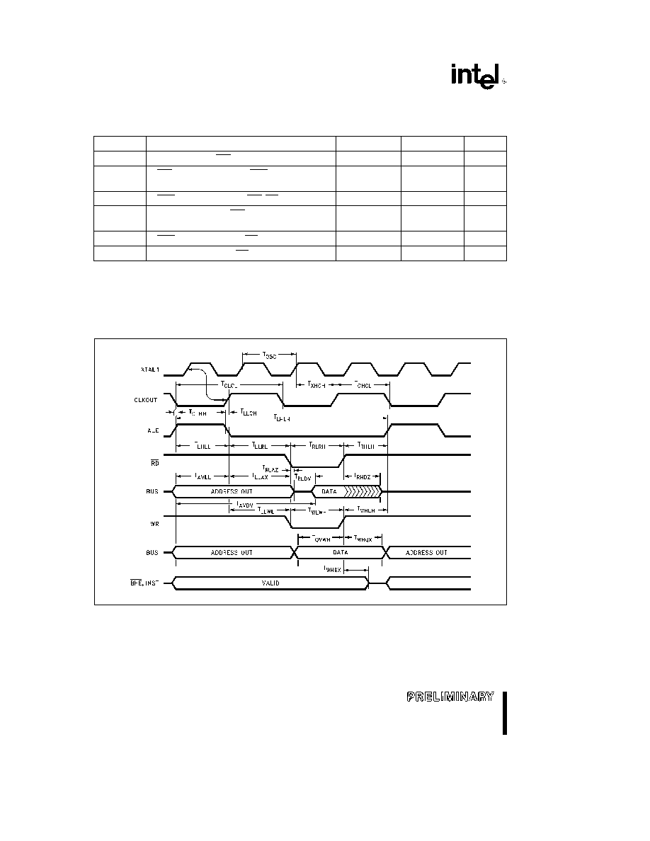
System Bus Timing
270679 � 4
10
AUTOMOTIVE 8XC196KB
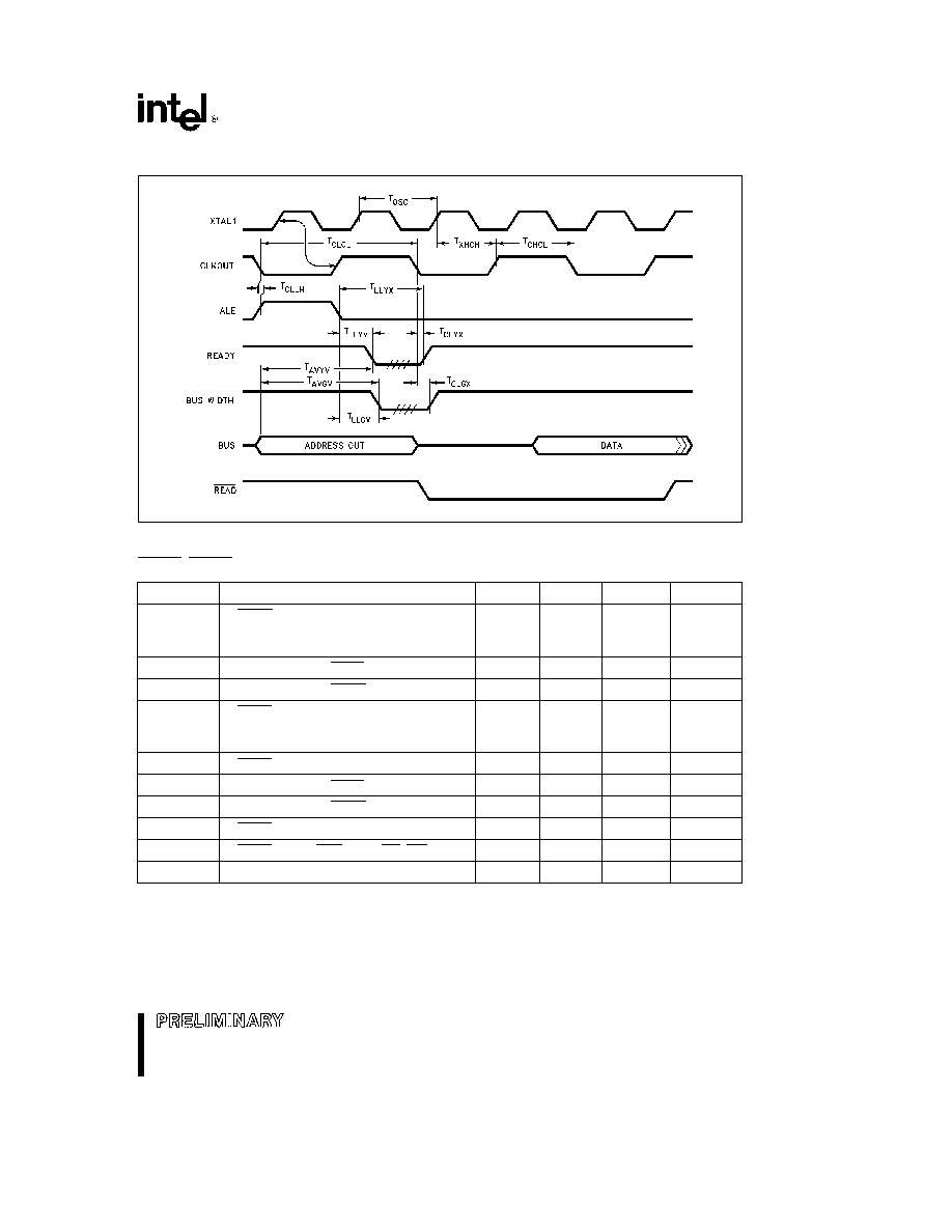
Ready Buswidth Timing
270679 � 5
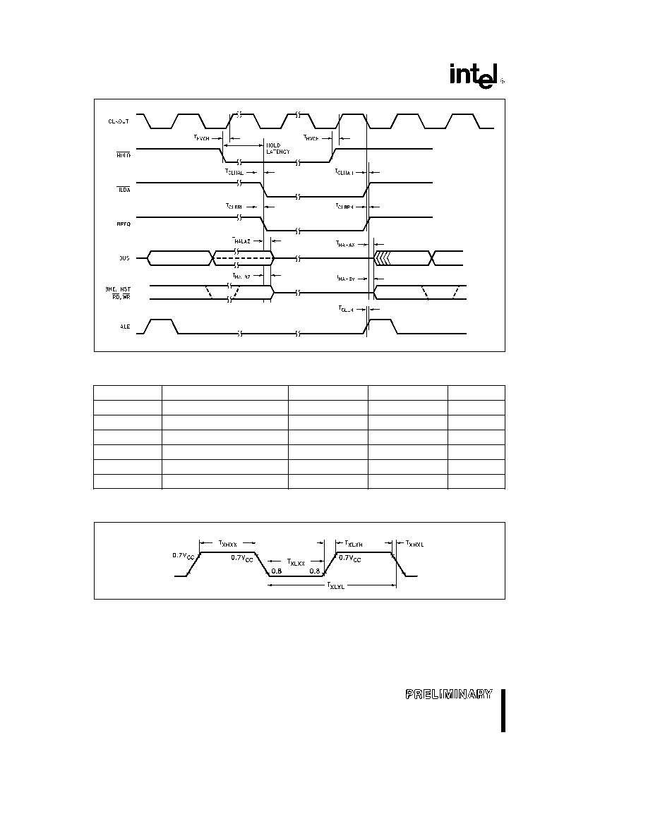
HOLD HLDA Timings
Symbol
Description
Min
Max
Units
Notes
T
HVCH
HOLD Setup
1
80C196KB
75
ns
83C196KB
85
T
CLHAL
CLKOUT Low to HLDA Low
b
15
15
ns
T
CLBRL
CLKOUT Low to BREQ Low
b
15
15
ns
T
HALAZ
HLDA Low to Address Float
80C196KB
15
ns
83C196KB
20
T
HALBZ
HLDA Low to BHE INST RD WR Float
ns
T
CLHAH
CLKOUT Low to HLDA High
b
15
15
ns
T
CLBRH
CLKOUT Low to BREQ High
b
15
15
ns
T
HAHAX
HLDA High to Address No Longer Float
b
5
ns
T
HAHBV
HLDA High to BHE INST RD WR Valid
b
20
ns
T
CLLH
CLKOUT Low to ALE High
b
5
15
ns
NOTE
1 To guarantee recognition at next clock
11
AUTOMOTIVE 8XC196KB
270679 � 27
External Clock Drive
Symbol
Parameter
Min
Max
Units
1 T
XLXL
Oscillator Frequency
3 5
16
MHz
T
XLXL
Oscillator Period (T
OSC
)
62 5
286
ns
T
XHXX
High Time
T
OSC
b
51
ns
T
XLXX
Low Time
T
OSC
b
51
ns
T
XLXH
Rise Time
T
OSC
b
73
ns
T
XHXL
Fall Time
T
OSC
b
73
ns
EXTERNAL CLOCK DRIVE WAVEFORMS
270679 � 6
12

AUTOMOTIVE 8XC196KB
AC TESTING INPUT OUTPUT WAVEFORMS
270679 � 7
AC Testing inputs are driven at 2 4V for logic ``1'' and 0 45V for a
logic ``0'' Timing measurements are made at 2 0V for a logic ``1''
and 0 8V for logic ``0''
FLOAT WAVEFORMS
270679 � 8
For timing purposes a port pin is no longer floating when a 100
mV change from load voltage occurs and begins to float when a
100 mV change from the loading V
OH
V
OL
level occurs I
OL
I
OH
s
g
15 mA
EXPLANATION OF AC SYMBOLS
Each symbol is two pairs of letters prefixed by ``t'' for
time The characters in a pair indicate a signal and
its condition respectively Symbols represent the
time between the two signal condition points
Conditions
Signals
H
High
A
Address
L
ALE ADV
L
Low
B
BHE
R
RD
V
Valid
C
CLKOUT W
WR WRH WRI
X
No Longer Valid D
Data
X
XTAL1
Z
Floating
G
Buswidth
Y
Ready
AC CHARACTERISTICS
SERIAL PORT
SHIFT REGISTER MODE
SERIAL PORT TIMING
SHIFT REGISTER MODE
Test Conditions T
C
e b
40 C to a125 C V
CC
e
5 0V
g
10% V
SS
e
0 0V Load Capacitance e 80 pF
Symbol
Parameter
Min
Max
Unit
T
XLXL
Serial Port Clock Period
(9)
6 T
OSC
4 T
OSC
ns
T
XLXH
Serial Port Clock Falling Edge
4 T
OSC
b
50 2 T
OSC
b
50 4 T
OSC
a
50 2 T
OSC
b
50 ns
to Rising Edge
(9)
T
QVXH
Output Data Setup to Clock Rising Edge
2 T
OSC
b
50
ns
T
XHQX
Output Data Hold after Clock Rising Edge
2 T
OSC
b
50
ns
T
XHQV
Next Output Data Valid
2 T
OSC
a
50
ns
after Clock Rising Edge
T
DVXH
Input Data Setup to Clock Rising Edge
T
OSC
a
50
ns
T
XHDX
(8)
Input Data Hold after Clock Rising Edge
0
ns
T
XHQZ
(8)
Last Clock Rising to Output Float
T
OSC
ns
NOTES
8 Parameter not tested
9 Baud Rate Register
t
8002H Baud Rate Register
e
8001H
13
AUTOMOTIVE 8XC196KB
A to D CHARACTERISTICS
There are two modes of A D operation with and
without clock prescaler The modes are shown in the
table below In mode 2 with the clock prescaler dis-
abled the maximum XTAL1 frequency is 8 0 MHz
Accuracy will degrade at higher frequencies in this
mode The frequency divider option is provided to
obtain higher accuracy outside of the currently spec-
ified operating conditions
The converter is ratiometric so the absolute accura-
cy is directly dependent on the accuracy and stability
of V
REF
V
REF
must be close to V
CC
since it supplies
both the resister ladder and the digital section of the
converter
A D Converter Specifications
The specifications given below assume adherence
to the operating conditions section of this data
sheet Testing is performed in mode 2 with V
REF
e
5 12V and 8 MHz operating clock frequency
WAVEFORM
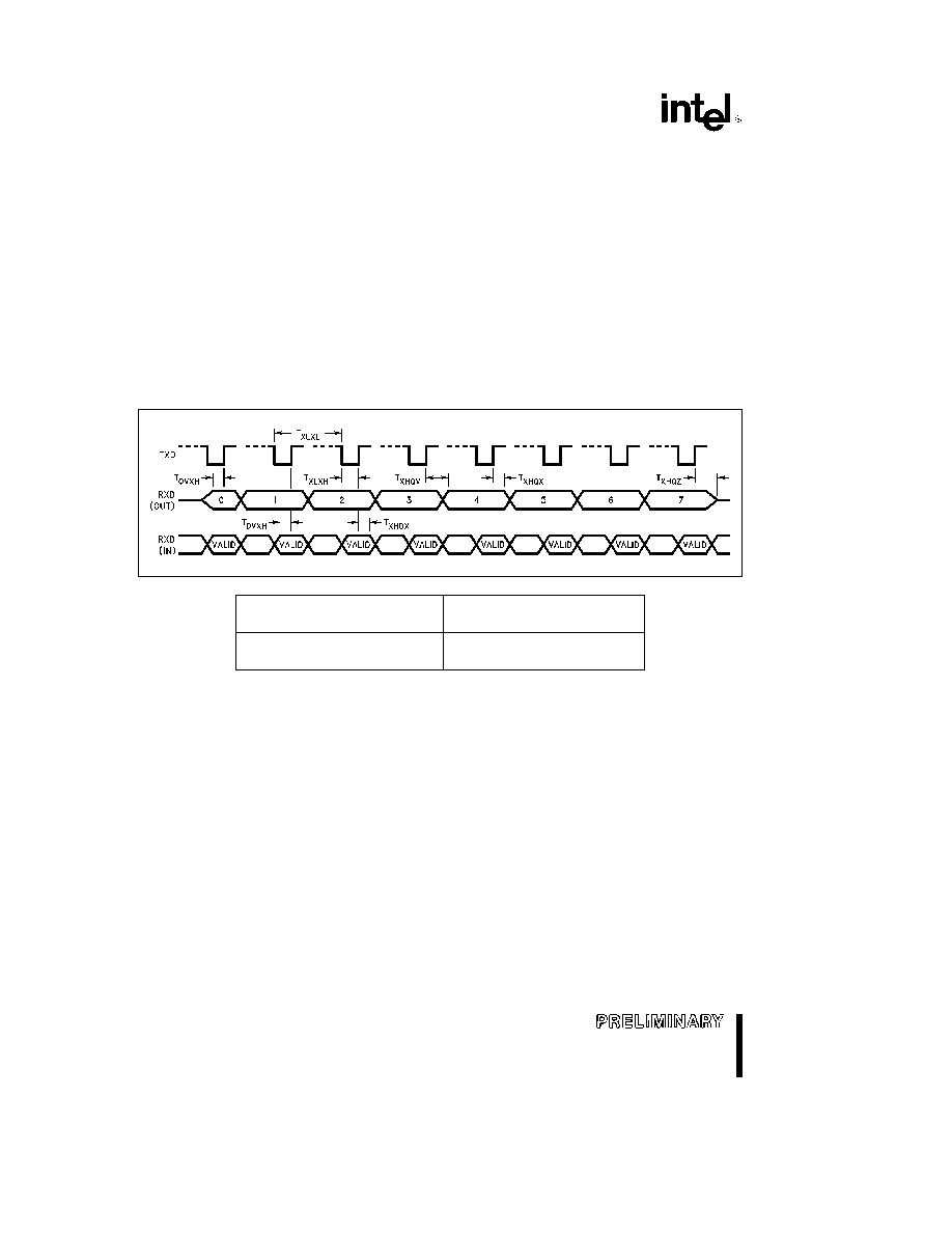
SERIAL PORT
SHIFT REGISTER MODE
SERIAL PORT WAVEFORM
SHIFT REGISTER MODE
270679 � 28
Clock Prescaler ON
Clock Prescaler OFF
IOC2 4 e 0
IOC2 4 e 1
Mode 1
158 States for Execution
Mode 2
91 States for Execution
26 33 ms
12 MHz
22 75 ms
8 MHz (Maximum)
NOTE
IOC2 3
e
0 The No Sample and Hold feature is not available on the 8XC196KB device
14

AUTOMOTIVE 8XC196KB
Parameter
Typical
(1)
Minimum
Maximum
Units
Resolution
512
1024
Level
9
10
Bits
Absolute Error
0
g
6
LSBs
Full Scale Error
0 25
g
0 5
LSBs
Zero Offset Error
b
0 25
g
0 5
LSBs
Non-Linearity
1 5
g
2 5
0
g
4
LSBs
Differential Non-Linearity
l
b
1
a
2
LSBs
Channel-to-Channel Matching
g
0 1
0
g
1
LSBs
Repeatability
g
0 25
LSBs
(1)
Temperature Coefficients
Offset
0 009
LSB C
(1)
Full Scale
0 009
LSB C
(1)
Differential Non-Linearity
0 009
LSB C
(1)
Off Isolation
b
60
dB
(1 2 4)
Feedthrough
b
60
dB
(1 2)
V
CC
Power Supply Rejection
b
60
dB
(1 2)
Input Resistance
1K
5K
X
(1)
DC Input Leakage
0
3
m
A
Sample Time (Prescaler on off)
15 8
States (3)
Input Capacitance
3
pF
NOTES
These values are expected for most parts at 25 C but are not tested or guaranteed
An ``LSB'' as used here has a value of approximately 5 mV (See Automotive Handbook for A D glossary of terms
1 These values are not tested in production and are based on theoretical estimates and or laboratory test
2 DC to 100 KHz
3 One state
e
125 ns
16 MHz 333 ns
6 MHz
4 Multiplexer Break-Before-Make Guaranteed
80C196KB FUNCTIONAL DEVIATIONS
The 80C196KB has the following problems
1 The HSI unit has two errata one dealing with res-
olution and the other with first entries into the
FIFO
The HSI resolution is 9 states instead of 8 states
Events on the same line may be lost if they occur
faster than once every 9 state times
There is a mismatch between the 9 state time HSI
resolution and the 8 state time timer This causes
one time value to be unused every 9 timer counts
Events may receive a time-tag one count later
than expected because of this ``skipped'' time val-
ue
If the first two events into an empty FIFO (not
including the Holding Register) occur in the same
internal phase both are recorded with one time-
tag Otherwise if the second event occurs within
9 states after the first its time-tag is one count
later than the first's If this is the ``skipped'' time
value the second event's time-tag is 2 counts lat-
er than the first's
If the FIFO and Holding Register are empty the
first event will transfer into the Holding Register
after 8 state times leaving the FIFO empty again
If the second event occurs after this time it will
act as a new first event into an empty FIFO
2 If an A D conversion in progress is aborted by
starting a new A D conversion results of the sec-
ond conversion may be inaccurate
15

AUTOMOTIVE 8XC196KB
The work-around is to wait for the conversion in
progress to finish before starting the second con-
version Polling or an interrupt will detect the con-
version completion
3 If the unsigned divide instruction (word or byte) is
in the queue as HOLD or READY is asserted the
result may be incorrect
TechBit (MC1791)
(B-step only )
DIFFERENCES BETWEEN THE
80C196KA AND THE 80C196KB
The 8XC196KB is identical to 8XC196KA except for
the following differences
1 ALE is high after reset on the 80C196KB instead
of low as on the 80C196KA
2 The DJNZW instruction is not guaranteed to work
on the 80C196KB (A-step only )
3 The HOLD HLDA bus protocol is available on the
80C196KB
CONVERTING FROM OTHER 8096BH
FAMILY PRODUCTS TO THE
80C196KB
The following list of suggestions for designing an
809XBH system will yield a design that is easily con-
verted to the 80C196KB
1 Do not base critical timing loops on instruction or
peripheral execution times
2 Use equate statements to set all timing parame-
ters including the baud rate
3 Do not base hardware timings on CLKOUT or
XTAL1 The timings of the 80C196KB are differ-
ent than those of the 8X9XBH but they will func-
tion with standard ROM EPROM Peripheral type
memory systems
4 Make sure all inputs are tied high or low and not
left floating
5 Indexed and indirect operations relative to the
stack pointer (SP) work differently on the
80C196KB than on the 8096BH On the 8096BH
the address is calculated based on the un-updat-
ed version of the stack pointer The 80C196KB
uses the updated version The offset for POP SP
and POP nn SP instructions may need to be
changed by a count of 2
6 The V
PD
pin on the 8096BH has changed to a
V
SS
pin on the 80C196KB
OTHER DESIGN CONSIDERATIONS
(KB B-0 to KB C-1)
1 The NMI pin on the KB ROM (C-1) has a weak
pulldown I
IH1
max is 100 mA The KB ROM (B-0)
did not have a pulldown on NMI If KB ROM (B-0)
designs have NMI tied to V
CC
the NMI pin must
be tied to V
SS
If NMI is tied to V
SS
or is floating
it is okay
2 The ALE RD and INST pins on the KB ROM
(C-1) have stronger pullups during RESET than
on the KB ROM (B-0) I
IL1
is b7 mA on the KB
ROM (C-1) compared to b1 2 mA on the KB
ROM (B-0) Designs which pull these pins low to
enter ONCE mode must have strong enough pull-
downs to overcome the pullups
3 Pin on the PLCC package on the KB ROM (B-0)
was the CDE pin That function did not work so
the pin was assigned to V
SS
On the KB ROM
(C-1) this pin is tied directly to V
SS
on the device
and MUST be tied to V
SS
externally
4 Several AC DC specifications have changed
(See Data Sheet Revision History review them
carefully )
16

AUTOMOTIVE 8XC196KB
DATA SHEET REVISION HISTORY
This is the -005 revision of the 8XC196KB data
sheet and is valid for devices marked with a ``F'' or
``G'' at the end of the topside tracking number The
following differences exist between the -004 revision
and the -005 revision
1 All performance related data is now quoted at
16 MHz The maximum clock rate has changed
from 12 MHz to 16 MHz
2 Max power dissipation changes from 0 43W to
1 5W
3 I
CC
max has changed from 60 mA to 70 mA
4 I
CC
typical has changed from 40 mA to 50 mA
5 I
REF
typical has changed from 1 mA to 2 mA
6 I
IDLE
has changed from 25 mA to 35 mA
7 V
IH2
min has changed from 2 4V to 2 5V
8 V
OH1
test condition for V
CC
b
0 3V has changed
from b7 mA to b15 mA
9 I
TL
has changed from b650 mA to b800 mA
10 I
IL1
has changed from b1 2 mA to b9 mA
11 I
IL1
now only applies to ALE RD and INST
12 R
RST
max has changed from 100 KX to 50 KX
13 Added spec for RESET pin hysteresis and I
IL2
for WR P2 0 and BHE
14 T
AVYV
has changed from 2 T
OSC
b
85 ns to
2 T
OSC
b
75 ns
15 T
LLYV
has changed from T
OSC
b
72 ns to T
OSC
b
60 ns
16 T
AVGV
has changed from 2 T
OSC
b
85 ns to
2 T
OSC
b
75 ns
17 T
AVDV
has changed from 3 T
OSC
b
65 ns to
3 T
OSC
b
55 ns
18 F
XTAL
max has changed from 12 MHz to
16 MHz
19 T
OSC
min has changed from 83 ns to 62 5 ns
20 T
XHCH
min has changed from 40 ns to 20 ns
21 T
CLLH
min max has changed from b5 ns 15 ns
to b10 ns 10 ns
22 T
LHLL
min max
has
changed
from
T
OSC
g
12 ns to T
OSC
g
10 ns
23 T
AVLL
has changed from T
OSC
b
20 ns to T
OSC
b
30 ns
24 T
LLRL
has changed from T
OSC
b
40 ns to T
OSC
b
35 ns
25 T
RLCL
min max has changed from 5 ns 30 ns
to 4 ns 25 ns
26 T
RLRH
has changed from T
OSC
b
5 ns to T
OSC
b
10 ns
27 T
RLAZ
has changed from 12 ns to 5 ns
28 T
CHWH
min max has changed from b10 ns
10 ns to b5 ns 15 ns
29 T
WLWH
min max has changed from T
OSC
b
30 ns to T
OSC
b
15 ns
30 T
WHQX
has changed from T
OSC
b
10 ns to
T
OSC
b
15 ns
31 T
WHLH
min max has changed from T
OSC
b
10 ns T
OSC
a
15 ns to T
OSC
b
20 ns T
OSC
a
10 ns
32 T
WHBX
has changed from T
OSC
b
10 ns to
T
OSC
b
15 ns
33 T
WHAX
has changed from T
OSC
b
50 ns to
T
OSC
b
30 ns
34 T
RHAX
has changed from T
OSC
b
50 ns to
T
OSC
b
25 ns
35 Functional deviation number 1 has been re-
moved (DJWZ is now functional)
36 Functional deviation number 3 has been re-
moved (SIO framing flag now works correctly)
37 Functional deviation number 5 has been re-
moved (SIO RI now correctly generated)
38 Functional deviation number 6 has been cor-
rected The divide during HOLD bug has been
fixed
39 The section ``Other Design Considerations KB
B-0 to KB C-1'' has been added
17