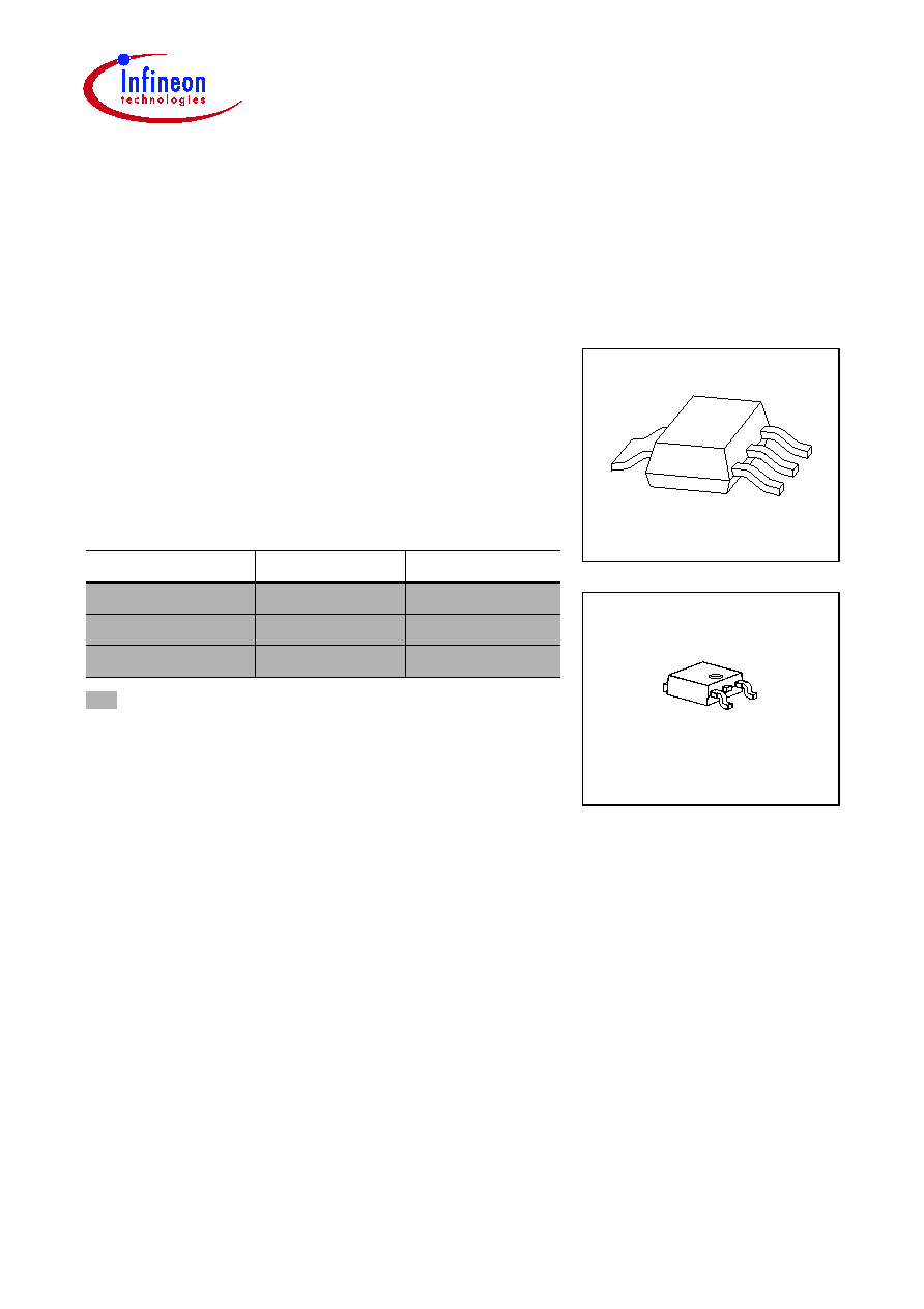
SOT-223
P-TO252-3-1
Voltage Regulator
TLE 4274 / 3.3V;2.5V
Data Sheet Rev. 2.1
1
2000-10-10
Functional Description
The TLE 4274 / 3.3V;2.5V is a voltage regulator available in a SOT223 and TO252
package. The IC regulates an input voltage up to 40 V to
V
Qrated
= 3.3 V/2.5 V. The
maximum output current is 400 mA. The IC is short-circuit proof and has a shutdown
circuit protecting it against over temperature. The TLE 4274 is also available as 5 V,
8.5 V and 10 V version. Please refer to the data sheet TLE 4274.
Features
· Output voltage: 3.3 V/2.5 V
±
4 %
· Current capability 400 mA
· Very low current consumption
· Short-circuit proof
· Reverse polarity proof
· Suitable for use in automotive electronics
SMD = Surface Mounted Device
w
New type
Type
Ordering Code Package
TLE 4274 GSV 33 Q67006-A9289 P-SOT223-4-1
w
TLE 4274 DV 33
Q67006-A9348 P-TO252-3-1
w
TLE 4274 GSV 25 Q67006-A9359 P-SOT223-4-1
TLE 4274 / 3.3V;2.5V
Data Sheet Rev. 2.1
2
2000-10-10
Dimensioning Information on External Components
The input capacitor
C
I
is necessary for compensating line influences. Using a resistor of
approx. 1
in series with
C
I
, the oscillating of input inductivity and input capacitance can
be damped. The output capacitor
C
Q
is necessary for the stability of the regulation circuit.
Stability is guaranteed for capacities
C
Q
10
µ
F with an ESR of
2.5
within the
operating temperature range.
Circuit Description
The control amplifier compares a reference voltage to a voltage that is proportional to the
output voltage and drives the base of the series transistor via a buffer. Saturation control
as a function of the load current prevents any oversaturation of the power element. The
IC also includes a number of internal circuits for protection against:
· Overload,
· Overtemperature,
· Reverse polarity.
Figure 1
Pin Configuration (top view)
Pin Definitions and Functions
Pin No.
Symbol
Function
1
I
Input; block to ground directly at the IC with a ceramic
capacitor.
2, 4
GND
Ground; P-TO252-3-1: internally connected to heatsink
3
Q
Output; block to ground with capacitor
C
Q
10
µ
F, ESR
2.5
AEP02561
1
3
Q
GND
P-SOT223-4-1
1
2
3
4
GND
GND
AEP02282
Q
P-TO252-3-1 (D-PAK)

TLE 4274 / 3.3V;2.5V
Data Sheet Rev. 2.1
3
2000-10-10
Figure 2
Block Diagram
1
AEB02283
GND
2
Q
3
Bandgap
Reference
Control
Amplifier
Sensor
Temperature
Buffer
Saturation
Control and
Protection
Circuit
TLE 4274 / 3.3V;2.5V
Data Sheet Rev. 2.1
4
2000-10-10
Note: Maximum ratings are absolute ratings; exceeding any one of these values may
cause irreversible damage to the integrated circut.
Absolute Maximum Ratings
T
j
= 40 to 150
°
C
Parameter
Symbol
Limit Values
Unit Test Condition
min.
max.
Voltage Regulator
Input
Voltage
V
I
42
45
V
Current
I
I
Internally limited
Output
Voltage
V
Q
1.0
40
V
Current
I
Q
Internally limited
Ground
Current
I
GND
100
mA
Temperature
Junction temperature
T
j
150
°
C
Storage temperature
T
stg
50
150
°
C
Operating Range
Parameter
Symbol
Limit Values
Unit Remarks
min.
max.
Input voltage
V
I
4.7
40
V
Junction temperature
T
j
40
150
°
C
Thermal Resistance
Junction ambient
R
thja
100
K/W SOT223
1)
Junction ambient
R
thja
70
K/W TO252
2)
Junction case
R
thjc
25
K/W SOT223
Junction case
R
thjc
4
K/W TO252
1)
soldered in, 1 cm
2
copper area at pin 4, FR4
2)
soldered in, minimal footprint, FR4

TLE 4274 / 3.3V;2.5V
Data Sheet Rev. 2.1
5
2000-10-10
Characteristics
V
I
= 6 V; 40
°
C <
T
j
< 150
°
C (unless otherwise specified)
Parameter
Symbol
Limit Values
Unit
Measuring Condition
min.
typ.
max.
Output voltage
V33-Version
V
Q
3.17
3.3
3.44
V
5 mA <
I
Q
< 400 mA
4.7 V <
V
I
< 28 V
Output voltage
V33-Version
V
Q
3.17
3.3
3.44
V
5 mA <
I
Q
< 200 mA
4.7 V <
V
I
< 40 V
Output voltage
V25-Version
V
Q
2.4
2.5
2.6
V
5 mA <
I
Q
< 400 mA
4.7 V <
V
I
< 28 V
Output voltage
V25-Version
V
Q
2.4
2.5
2.6
V
5 mA <
I
Q
< 200 mA
4.7 V <
V
I
< 40 V
Output current
limitation
1)
I
Q
400
600
mA
Current consumption;
I
q
=
I
I
I
Q
I
q
100
220
µ
A
I
Q
= 1 mA
Current consumption;
I
q
=
I
I
I
Q
I
q
8
15
mA
I
Q
= 250 mA
Current consumption;
I
q
=
I
I
I
Q
I
q
20
30
mA
I
Q
= 400 mA
Drop voltage
1)
V33-Version
V
dr
0.7
1.2
V
I
Q
= 300 mA
V
dr
=
V
I
V
Q
Drop voltage
1)
V25-Version
V
dr
1.0
2.0
V
I
Q
= 300 mA
V
dr
=
V
I
V
Q
Load regulation
V
Q
40
70
mV
I
Q
= 5 mA to
300 mA;
V
I
= 6 V
Line regulation
V
Q
10
25
mV
V
l
= 12 V to 32 V
I
Q
= 5 mA
Power supply ripple
rejection
PSRR
60
dB
f
r
= 100 Hz;
V
r
= 0.5
V
SS
Temperature output
voltage drift
0.5
mV/K
1)
Measured when the output voltage
V
Q
has dropped 100 mV from the nominal value obtained at
V
I
= 6 V.
d
V
Q
d
T
----------