
N e v e r s t o p t h i n k i n g .
M i c r o c o n t r o l l e r s
D a t a S h e e t , V 2 . 3 , N o v . 2 0 0 3
T C 1 1 I B
3 2 - B i t S i n g l e - C h i p M i c r o c o n t r o l l e r

Edition 2003-11
Published by Infineon Technologies AG,
St.-Martin-Strasse 53,
D-81541 M�nchen, Germany
�
Infineon Technologies AG 2003.
All Rights Reserved.
Attention please!
The information herein is given to describe certain components and shall not be considered as warranted
characteristics.
Terms of delivery and rights to technical change reserved.
We hereby disclaim any and all warranties, including but not limited to warranties of non-infringement, regarding
circuits, descriptions and charts stated herein.
Infineon Technologies is an approved CECC manufacturer.
Information
For further information on technology, delivery terms and conditions and prices please contact your nearest
Infineon Technologies Office in Germany or our Infineon Technologies Representatives worldwide (see address
list).
Warnings
Due to technical requirements components may contain dangerous substances. For information on the types in
question please contact your nearest Infineon Technologies Office.
Infineon Technologies Components may only be used in life-support devices or systems with the express written
approval of Infineon Technologies, if a failure of such components can reasonably be expected to cause the failure
of that life-support device or system, or to affect the safety or effectiveness of that device or system. Life support
devices or systems are intended to be implanted in the human body, or to support and/or maintain and sustain
and/or protect human life. If they fail, it is reasonable to assume that the health of the user or other persons may
be endangered.

M i c r o c o n t r o l l e r s
D a t a S h e e t , V 2 . 3 , N o v . 2 0 0 3
N e v e r s t o p t h i n k i n g .
T C 1 1 I B
3 2 - B i t S i n g l e - C h i p M i c r o c o n t r o l l e r
TC11IB
Advance Information
Revision History:
2003-11
V2.3
Previous Version:
V1.1, 2002-03
V1.2, 2002-04
V1.3, 2002-09
V2.0, 2002-12
V2.1, 2003-02
V2.2, 2003-07
Page
Subjects (major changes since last revision)
71
Power supply current is updated.
We Listen to Your Comments
Any information within this document that you feel is wrong, unclear or missing at all?
Your feedback will help us to continuously improve the quality of this document.
Please send your proposal (including a reference to this document) to:
mcdocu.comments@infineon.com

Data Sheet
1
V2.3, 2003-11
TC11IB
32-Bit Single-Chip Microcontroller
TriCore Family
Advance Information
� High Performance 32-bit TriCore CPU with 4-Stage Pipeline running at 96MHz Clock
� Dual Issue super-scalar implementation
� MAC Instruction maximum triple issue
� Circular Buffer and bit-reverse addressing modes for DSP algorithms
� Flexible multi-master interrupt system
� Very fast interrupt response time
� Hardware controlled context switch for task switch and interrupts
� Windows CE compliant Memory Management Unit (MMU)
� 64 kByte of on-chip SRAM for data and time critical code
� Independent Peripheral Control Processor (PCP) for low level driver support with
20 kByte code / parameter memory
� eDRAM Local Memory Unit (LMU) with 512 KBytes Code/data Memory.
� ComDRAM with 1MBytes DRAM Memory
� High Performance Local Memory Bus (LMB) for fast access between Caches and on-
local memories and Fast-FPI Interface.
� Two On-chip Flexible Peripheral Interface Buses (Fast FPI Bus and Slow FPI Bus) for
interconnections of functional units
� Flexible External Bus Interface Unit (EBU) used for communication with external data
memories such as PC 100 SDRAM, Burst Flash and SRAM etc. and external
peripheral units, including Intel style and Motorola style peripherals.
� On-Chip Peripheral Units
� Two Multifunctional General Purpose Timer Units (GPTU0 & GPTU1) with three 32-
bit timer/counters each
� Asynchronous/Synchronous Serial Channels (ASC) with IrDA data transmission,
receive/transmit FIFOs, parity, framing and overrun error detection
� High Speed Synchronous Serial Channels (SSC) with programmable data length
and shift direction
� Asynchronous Serial Interface (16X50) with programmable XON/XOFF characters,
Baudrate generator, receive/transmit FIFOs and standard modem interface
support.
� 16 MHz MultiMediaCard Interface (MMCI), a glueless interface to MultiMediaCard
Bus, with bus clock generation, CRC protection and up to 2 MByte/s data
communication.
� Fast Ethernet Controller with 10/100 Mbps MII-Based physical devices support.
� PCI V2.2 Interface with PCI Bus Power Management and DMA data transfer.
� Watchdog Timer and System Timer
� Six 16-bit digital I/O ports
� On-Chip Debug Support (OCDS)

TC11IB
Data Sheet
2
V2.3, 2003-11
� Power Management System
� Clock Generation Unit with PLL
� Ambient temperature under bias: -25 �C to +85 �C
� P-BGA-388-2 package

TC11IB
Data Sheet
3
V2.3, 2003-11
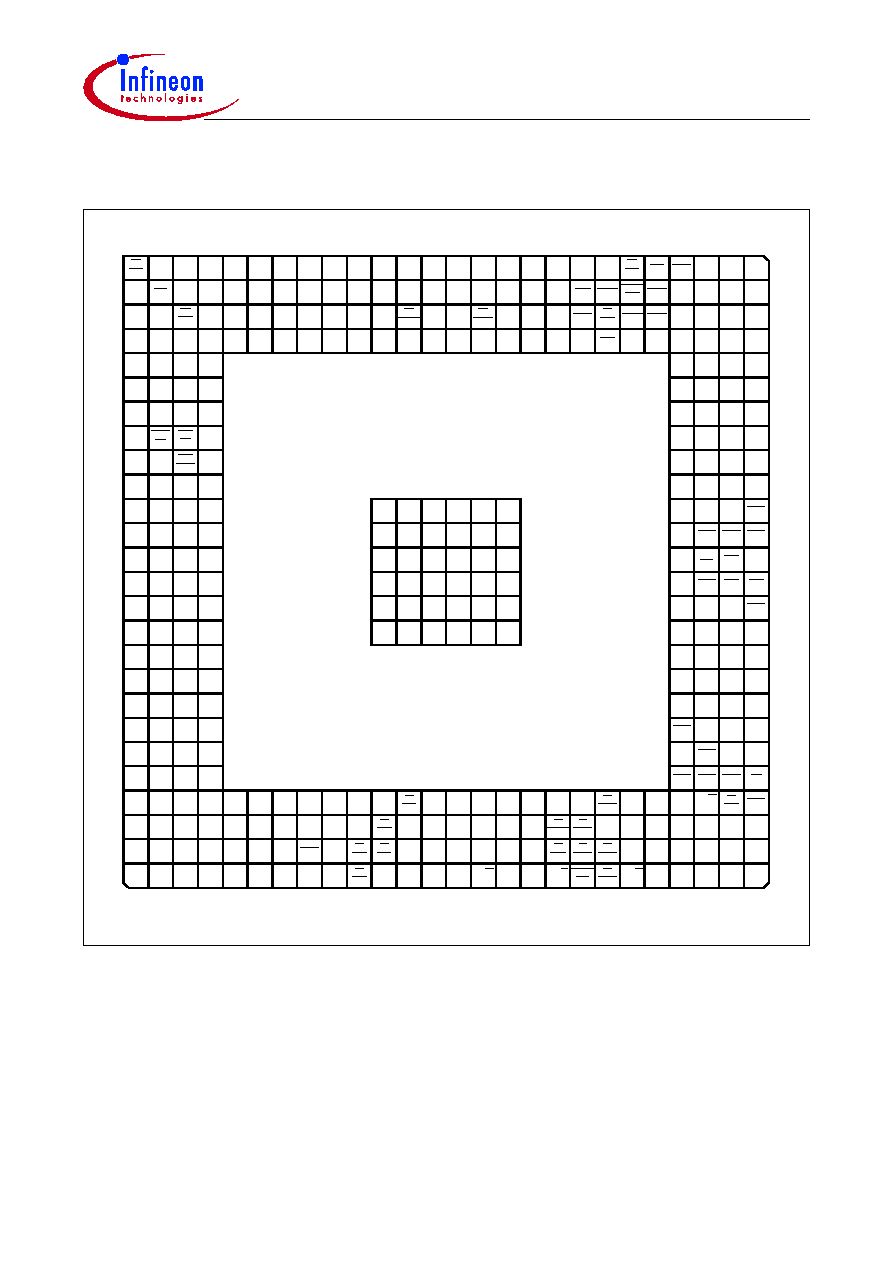
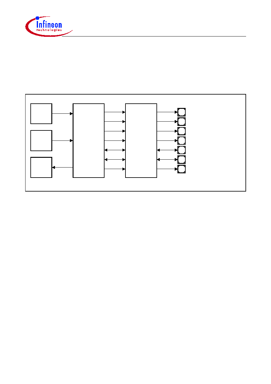
Block Diagram
Figure 1
TC11IB Block Diagram
M
C
B
0493
9
PC
P
In
t
e
rru
p
t
4
K Da
t
a
S
R
A
M
1
6
K Co
d
e
S
R
A
M
OCD
S
FP
I Inte
rfa
ce
Bo
o
t
-
R
O
M
16
K
b
y
t
es
MM
C
I
1
6x50
XO
N
/
XO
F
F
ASC
FI
FO
,
Ir
D
A
SS
C
GP
T
U
1
3 T
i
m
e
r
s
GP
T
U
0
3 T
i
m
e
r
s
SC
U
(P
W
R
)
Po
w
e
r
M
anag
em
en
t
,
W
a
t
c
hd
og T
i
m
e
r
,
Re
s
e
t
BCU1
Sl
o
w
F
P
I
BU
S
Ce
r
b
e
r
u
s
JT
A
G
PL
L
96
&
4
8
M
H
z
Tr
i
C
or
e
1
.
3
CP
U
In
t
e
r
r
u
p
t
Tr
ac
e
&
OC
D
S
PM
U
(
P
r
o
g
r
a
m
M
e
m
o
r
y
U
n
it
)
24
K
B
S
c
r
a
t
c
h P
ad
R
A
M
8
K
B
I
n
st
r
u
ct
i
o
n
C
a
ch
e
LM
U
512 K
B
e
DRA
M
J
T
A
G
I/O
XTAL
2
XTAL
1
5
C
ont
r
o
l
BR
K
O
U
T
BR
K
I
N
8
O
CDS
E
O
CDS
2
FF
I
Br
i
d
g
e
16
8
DM
U
(
D
a
t
a
M
e
m
o
r
y
U
n
it
)
24
K
B
S
c
r
a
t
c
h P
ad
R
A
M
8
K
B
D
a
t
a
C
a
c
h
e
Co
m
D
R
A
M
1 M
B
,
96
M
H
z
BCU
0
F
a
s
t
F
P
I
B
U
S
F
a
st
F
P
I
B
u
s 96 M
H
z
,
3
2
B
i
t
LF
I
B
r
i
dge
EB
U_
L
M
B
Fa
st
Et
h
e
r
n
e
t
PC
I
V2
.
2
3
3
M
H
z
(
D
M
A
S
upp
or
t
)
+
P
o
w
e
r
M
a
n
agem
ent
8
3
2
8
3
1
PO
R
T
0
PO
R
T
1
PO
R
T
2
MD
I
O
Tx
C
L
K
Rx
CL
K
15
32
20
P
_
A
D
[
31:
0]
P
_
C
ont
r
o
l
PO
R
T
3
PO
R
T
4
PO
R
T
5
9
32
33
A
D
[
31:
0]
E
B
U_
Co
n
t
r
o
l
MM
U
24
A
[
23:
0]
LM
B
(
L
oc
al
M
e
m
o
r
y
B
u
s)
96
M
H
z
,
6
4
B
i
t
3
16
16
16
E
x
t
e
r
nal
In
te
r
r
u
p
ts
Ex
t
e
r
n
a
l
In
te
r
r
u
p
t
s
16
16
1
6
128
64
V
DD
1.
8-
3
.
3 V
V
SS
S
l
o
w
F
P
I
B
u
s
(
F
l
exi
b
l
e
P
e
r
i
p
h
e
r
a
l
I
n
t
e
r
f
ace)
48
M
H
z
,
32
B
i
t
T
C
1
1
IB
Bl
o
c
k
Di
a
g
r
a
m

TC11IB
Data Sheet
4
V2.3, 2003-11
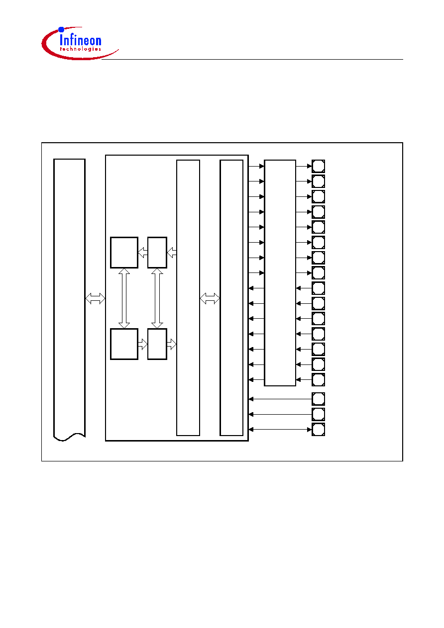
Logic Symbol
Figure 2
TC11IB Logic Symbol
M C B 0 4 9 4 5
TC 11IB
P ort 0 16-B it
S V M
W A IT
R D /W R
R D
C P U C LK
C F G [0:3]
N M I
H D R S T
P O R S T
V
S S
V
D D O S C
H O L D
R A S
A LE
B R E Q
H LD A
E B U C ontrol
A lternate F unctions
D igital C ircuitry
P ow er S upply
4
G eneral C ontrol
C A S
C S [0:6]
7
C S E M U
C S G LB
C S O V L
C S F P I
C K E
M R _ W
R M W
E B U C LK
B A A
A D V
A C LK
C M D E LA Y
M II_T xC LK
M II_R xC LK
M II_M D IO
T E S T M O D E
T M _C T R L1
T M _C T R L2
C LK 42
P LL96_C trl
P LL42_C trl
X T A L1
X T A L2
E thernet C lo ck
T E S T
V
S S O S C
V
D D P L L 9 6
V
S S P L L 9 6
V
D D P L L 4 2
V
S S P L L 4 2
O scillator / P LL
52
21
V
D D
V
D D P
20
V
D D D R A M
2
V
C O M R E F
V
L M U R E F
P _C LK 33
P _ID S E L
P _G N T
P _R E Q
P _P M E
P _IN T B
P _IN T A
P _LO C K
P _IR D Y
P _F R A M E
P _T R D Y
P _D E V S E L
P _S T O P
P _P E R R
P _S E R R
P _P A R
P _C /B E [0:3]
P _A D [0:31]
O C D S 2B R K [0:2]
O C D S 2P C [0:7]
O C D S 2P S [0:4 ]
O C D S /
JT A G
C ontrol
A [0:23 ]
B C [0:3]
A D [0:31]
P ort 1 16-B it
P ort 2 16-B it
P ort 3 16-B it
P ort 4 16-B it
P ort 5 16-B it
G P T U 0/1
S S C 0/1, M M C I,
A S C , 16x50
E thernet, M M C I
E xternal
Interrupts
M M C I
E B U C ontrol
O C D S / JT A G
C ontrol
P C I
TC11IB
Data Sheet
5
V2.3, 2003-11
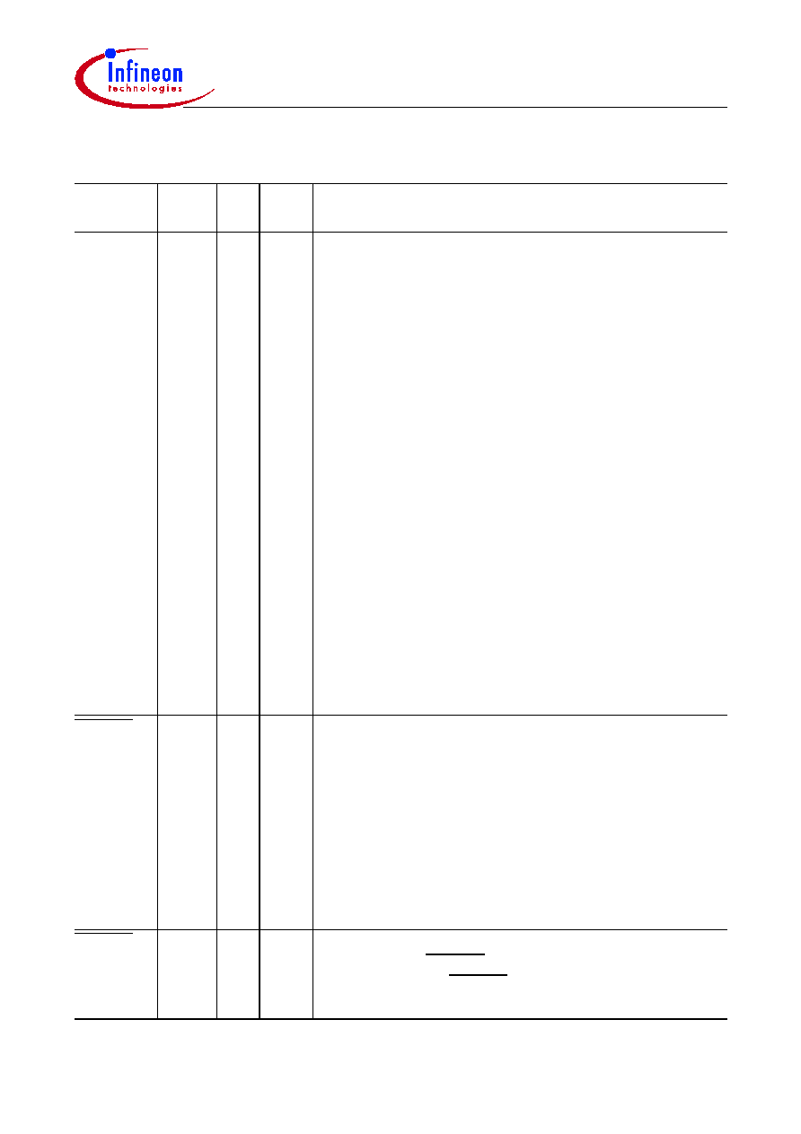
Pin Configuration
Figure 3
TC11IB Pinning: P-BGA-388 Package (top view)
M C P 0 4 9 5 0
A F
1
2
3
4
5
6
7
8
9
M II_
M D IO
10
11
12
13
X T A L2
14
15
X T A L1
16
17
P 2.3
18
19
20
21
B A A
22
23
R es er
v ed
P 1.15
H D
R S T
A
B
P LL96
C T R L
P 2.2
V
D D
O S C
C
C P U
C LK
A
B
C
D
V
S S
D
E
F
G
H
J
K
L
M
N
P
R
T
U
P 3.7
V
P 3.8
P 3.9
W
F
G
H
J
K
L
M
N
P
R
T
U
V
W
A C
E
A D
A D
A E
A E
P 5.0
A F
R es er
v ed
1
2
3
4
5
6
7
8
9
10
11
12
13
14
15
16
17
18
19
20
24
25
26
V
S S
V
S S
V
S S
V
S S
V
S S
V
S S
V
S S
V
S S
V
S S
V
S S
V
S S
V
S S
V
S S
V
S S
V
S S
V
S S
V
S S
V
S S
V
S S
V
S S
V
S S
V
S S
V
S S
V
S S
P 1.13
P 1.11
P 1.7
P 1.4
P 1.0
P 2.12
P 2.10
M II_
T x C LK
V
D D
P LL42
V
S S
P LL96
V
LM U
R E F
V
D D
D R A M
P 2.1
A LE
24
25
26
C S
G LB
H LD A
A [20]
A D [3 1]
A D [3 0] A D [29]
A [21]
A D [23]
B R E Q
C M D E
LA Y
C S F P I
A D V
P 2.5
P 2.7
V
D D
P LL96
P LL42
C T R L
V
D D
P 2.8
P 2.11
P 2.14
P 1.1
P 1.5
P 1.8
V
D D
P 1.14
O C D S
2P S [2]
N M I
O C D S
2P C [7]
P O
R S T
P 1.12
P 1.9
P 1.6
P 1.2
P 2.15
P 2.13
P 2.9
M II_
R x C LK
T M
C T R L2
V
S S
P LL42
V
S S O S C
T M
C T R L1
P 2.6
P 2.4
P 2.0
W A IT
C S
O V L
M R _W
H O LD
A [22]
A D [22] A D [2 1] A D [28]
A D [26]
A D [2 7]
A D [20]
V
S S
A [23]
V
D D
S V M
V
D D P
V
S S
V
D D
V
D D P
R es er
v ed
V
D D P
V
S S
C LK 42
V
D D P
V
D D
V
S S
V
D D P
P 1.3
V
D D
P 1.10
V
S S
O C D S
2P C [4]
O C D S
2P S [1]
O C D S
2P S [4]
O C D S
2P C [3]
O C D S
2P C [6]
O C D S
2P S [0]
O C D S
2P S [3]
O C D S
2P C [1]
O C D S
2P C [2]
O C D S
2P C [5]
V
D D
O C D S
2P C [0]
O C D S
2 B R K
[0]
O C D S
2B R K
[1]
O C D S
2B R K
[2]
V
D D
O C D S
_E
B R K
_IN
V
D D P
V
S S
B R K
_ O U T
C F G
[3]
C F G
[2]
P 0.0
C F G
[1]
C F G
[0]
V
D D
P 0.3
P 0.2
P 0.1
V
D D P
P 0.4
P 0.5
P 0.6
P 0.7
P 0.8
P 0.9
P 0.10
V
D D P
P 0.11
P 0.12
P 0.13
V
S S
P 0.14
P 0.15
P 3.0
P 3.1
P 3.2
V
D D
P 3.3
V
D D P
P 3.4
P 3.5
P 3.6
V
D D
P 3.10
P 3.11
V
D D P
Y
P 4.0
P 4.1
P 4.2
P 3.12
P 3.13
P 3.14
P 4.4
P 4.5
A A
A B
A C
P 3.15
P 4.3
P 4.6
P 4.8
P 4.9
P 4.7
P 5.3
P 5.10
V
D D P
V
D D P
P _
P M E
V
D D P
P _
ID S E L
V
D D P
V
S S
V
D D
V
S S
V
D D
V
S S
V
D D
V
S S
V
D D
V
D D
V
S S
V
D D P
P _
S T O P
V
D D
P _A D
[13]
V
S S
P _C /B E
[0]
C S
E M U
C S [1]
Y
A A
A B
A D [24]
A D [2 5]
A D [18]
A D [19]
V
D D
A D [15]
A D [1 6]
A D [17]
V
D D P
B C [2]
A D [0]
A D [1]
A D [13]
A D [1 4]
A D [6]
A D [7]
V
D D P
A D [11]
A D [1 2]
A D [5]
V
S S
A D [9]
A D [10]
A D [4]
V
D D
A D [8]
A D [3]
A D [2]
A C LK
B C [3]
B C [0]
B C [1]
V
S S
R D /
W R
C A S
E B U
C LK
V
D D P
R A S
C S [6]
C K E
A [17]
A [18]
A [19]
C S [5]
V
D D P
A [16]
A [15]
A [14]
V
D D
A [12]
A [11]
A [13]
V
S S
A [1]
A [9]
A [10]
V
D D P
A [2]
A [7]
A [8]
C S [4]
A [3]
A [4]
A [6]
V
D D
C S [3]
A [5]
A [0]
C S [0]
C S [2]
R M W
R D
21
22
23
P 4.10
P 4.11
P 4.14
P 5.2
P 5.6
P 5.9
P 5.13
T M S
T D I
V C O M
R E F
P _
G N T
P _A D
[30]
P _A D
[28]
P _A D
[26]
P _A D
[22]
P _A D
[20]
P _A D
[18]
P _
F R A M E
P _
T R D Y
P _
P A R
P _A D
[15]
P _A D
[11]
P _A D
[9]
P _A D
[6]
P _A D
[2]
P _A D
[0]
P 4.12
P 4.13
P 5.1
P 5.5
P 5.8
P 5.12
P 5.15
T R S T
T E S T
M O D E
P _
IN T A
P _
R E Q
P _A D
[29]
P _A D
[27]
P _A D
[24]
P _A D
[23]
P _A D
[19]
P _A D
[16]
P _
IR D Y
P _
LO C K
P _
S E R R
P _A D
[14]
P _A D
[10]
P _A D
[7]
P _A D
[4]
P _A D
[1]
R es er
v ed
P _C /B E
[1]
P _A D
[12]
P _A D
[8]
P _A D
[5]
P _A D
[3]
P _
P E R R
P _D E V
S E L
P _C /B E
[2]
P _A D
[25]
P _A D
[21]
P _A D
[17]
P _C /B E
[3]
V
D D
D R A M
P _A D
[31]
P _C L K
33
P _
IN T B
R e s er
v ed
T D O
T C K
P 4.15
P 5.4
P 5.7
P 5.11
P 5.14
V
S S
V
S S
V
S S
V
S S
V
S S
V
S S
V
S S
V
S S
V
S S
V
S S
V
S S
3 8 8 -P in P -B G A P a c ka g e P in C o n fig u ra tio n (to p vie w )
fo r T C 1 1 IB

TC11IB
Data Sheet
6
V2.3, 2003-11
Table 1
Pin Definitions and Functions
Symbol
Pin
In
Out
PU/
PD
1)
Functions
P0
P0.0
P0.1
P0.2
P0.3
P0.4
P0.5
P0.6
P0.7
P0.8
P0.9
P0.10
P0.11
P0.12
P0.13
P0.14
P0.15
K1
L3
L2
L1
M1
M2
M3
M4
N1
N2
N3
P1
P2
P3
R1
R2
I/O
I/O
I/O
I/O
I/O
I/O
I/O
I/O
I/O
I/O
I/O
I/O
I/O
I/O
I/O
I/O
I/O
PUB
PUB
PUB
PUB
PUC
PDC
PDC
PUC
PUC
PUC
PUC
PUC
Port 0
Port 0 serves as 16-bit general purpose I/O port, which
is also used as input/output for the General Purpose
Timer Units (GPTU0 & GPTU1)
GPTU0_IO0
GPTU0 I/O line 0
GPTU0_IO1
GPTU0 I/O line 1
GPTU0_IO2
GPTU0 I/O line 2
GPTU0_IO3
GPTU0 I/O line 3
GPTU0_IO4
GPTU0 I/O line 4
GPTU0_IO5
GPTU0 I/O line 5
GPTU0_IO6
GPTU0 I/O line 6
GPTU0_IO7
GPTU0 I/O line 7
GPTU1_IO0
GPTU1 I/O line 0
GPTU1_IO1
GPTU1 I/O line 1
GPTU1_IO2
GPTU1 I/O line 2
GPTU1_IO3
GPTU1 I/O line 3
GPTU1_IO4
GPTU1 I/O line 4
GPTU1_IO5
GPTU1 I/O line 5
GPTU1_IO6
GPTU1 I/O line 6
GPTU1_IO7
GPTU1 I/O line 7

TC11IB
Data Sheet
7
V2.3, 2003-11
P1
P1.0
P1.1
P1.2
P1.3
P1.4
P1.5
P1.6
P1.7
P1.8
P1.9
P1.10
P1.11
P1.12
P1.13
P1.14
P1.15
A7
B7
C7
D7
A6
B6
C6
A5
B5
C5
D5
A4
C4
A3
B3
A2
I/O
I/O
I/O
I/O
O
I/O
I/O
I/O
O
I
O
O
I
I
O
I
I
PUC
PUC
PUC
PUC
PUC
PUC
PUC
PUC
PUC
PUC
PUC
PUC
PUC
PUC
PUC
PUC
Port 1
Port 1 serves as 16-bit general purpose I/O port, which
also is used as input/output for the serial interfaces
(SSC,ASC,16X50) and MultiMediaCard Interface
(MMCI)
SCLK
SSC clock input/output line
MRST
SSC master receive / slave transmit
input/output
MTSR
SSC master transmit / slave receive
input/output
MMCI_CLK
MMCI clock output line
MMCI_CMD
MMCI command input/output line
MMCI_DAT
MMCI data input/output line
ASC_RXD
ASC receiver input/output line
ASC_TXD
ASC transmitter output line
16X50_RXD
16X50 receiver input line
16X50_TXD
16X50 transmitter output line
16X50_RTS
16X50 request to send output line
16X50_DCD
16X50 data carrier detection input line
16X50_DSR
16X50 data set ready input line
16X50_DTR
16X50 data terminal ready output line
16X50_CTS
16X50 clear to send input line
16X50_RI
16X50 ring indicator input line
Table 1
Pin Definitions and Functions(cont'd)
Symbol
Pin
In
Out
PU/
PD
1)
Functions

TC11IB
Data Sheet
8
V2.3, 2003-11
P2
P2.0
P2.1
P2.2
P2.3
P2.4
P2.5
P2.6
P2.7
P2.8
P2.9
P2.10
P2.11
P2.12
P2.13
P2.14
P2.15
C18
A19
B18
A18
C17
B17
C16
B16
B10
C10
A9
B9
A8
C9
B8
C8
I/O
O
O
O
O
O
O
O
O
I
I
I
I
I
I
I
I
PUC
PDC
PDC
PUC
PDC
PDC
PDC
PDC
PDC
Port 2
Port 2 serves as 16-bit general purpose I/O port, which
is also used as input/output for Ethernet controller and
MultiMediaCard (MMCI).
MII_TXD0
Ethernet controller transmit data output
line 0
MII_TXD1
Ethernet controller transmit data output
line 1
MII_TXD2
Ethernet controller transmit data output
line 2
MII_TXD3
Ethernet controller transmit data output
line 3
MII_TXER
Ethernet controller transmit error
output line
MII_TXEN
Ethernet controller transmit enable
output line
MII_MDC
Ethernet controller management data
clock output line
MMCI_VDDEN
MMCI power supply enable output line
MII_RXDV
Ethernet Controller receive data valid
input line
MII_CRS
Ethernet Controller carrier input line
MII_COL
Ethernet Controller collision input line
MII_RXD0
Ethernet Controller receive data input
line 0
MII_RXD1
Ethernet Controller receive data input
line 1
MII_RXD2
Ethernet Controller receive data input
line 2
MII_RXD3
Ethernet Controller receive data input
line 3
MII_RXER
Ethernet Controller receive error input
line
Table 1
Pin Definitions and Functions(cont'd)
Symbol
Pin
In
Out
PU/
PD
1)
Functions

TC11IB
Data Sheet
9
V2.3, 2003-11
P3
P3.0
P3.1
P3.2
P3.3
P3.4
P3.5
P3.6
P3.7
P3.8
P3.9
P3.10
P3.11
P3.12
P3.13
P3.14
P3.15
R3
R4
T1
T3
U1
U2
U3
V1
V2
V3
W2
W3
Y1
Y2
Y3
Y4
I/O
I
I
I
I
I
I
I
I
I
I
I
I
I
I
I
I
Port 3
Port 3 serves as 16-bit general purpose I/O port, which
is also used as input for external interrupts.
INT0
External interrupt input line 0
INT1
External interrupt input line 1
INT2
External interrupt input line 2
INT3
External interrupt input line 3
INT4
External interrupt input line 4
INT5
External interrupt input line 5
INT6
External interrupt input line 6
INT7
External interrupt input line 7
INT8
External interrupt input line 8
INT9
External interrupt input line 9
INT10
External interrupt input line 10
INT11
External interrupt input line 11
INT12
External interrupt input line 12
INT13
External interrupt input line 13
INT14
External interrupt input line 14
INT15
External interrupt input line 15
Table 1
Pin Definitions and Functions(cont'd)
Symbol
Pin
In
Out
PU/
PD
1)
Functions

TC11IB
Data Sheet
10
V2.3, 2003-11
P4
P4.0
P4.1
P4.2
P4.3
P4.4
P4.5
P4.6
P4.7
P4.8
P4.9
P4.10
P4.11
P4.12
P4.13
P4.14
P4.15
AA1
AA2
AA3
AB1
AB2
AB3
AB4
AC1
AC2
AC3
AD1
AD2
AE1
AE2
AD3
AF2
I/O
I
I
I
I
I
I
I
I
I/O
I/O
I/O
I/O
I/O
I/O
I/O
I/O
PDC
PDC
PDC
PDC
PUC
PUC
PUC
PUC
PUC
PUC
PUC
PUC
PUC
PUC
PUC
PUC
Port 4
Port 4 is used as general purpose I/O port, 8 pins of
which (P4.0 ~ P4.7) also serve as inputs for external
interrupts.
INT16
External interrupt input line 16
INT17
External interrupt input line 17
INT18
External interrupt input line 18
INT19
External interrupt input line 19
INT20
External interrupt input line 20
INT21
External interrupt input line 21
INT22
External interrupt input line 22
INT23
External interrupt input line 23
Table 1
Pin Definitions and Functions(cont'd)
Symbol
Pin
In
Out
PU/
PD
1)
Functions
TC11IB
Data Sheet
11
V2.3, 2003-11
P5
P5.0
P5.1
P5.2
P5.3
P5.4
P5.5
P5.6
P5.7
P5.8
P5.9
P5.10
P5.11
P5.12
P5.13
P5.14
P5.15
AF1
AE3
AD4
AC5
AF3
AE4
AD5
AF4
AE5
AD6
AC7
AF5
AE6
AD7
AF6
AE7
I/O
O
I/O
O
I/O
I/O
I/O
I/O
I/O
I/O
I/O
I/O
I/O
I/O
I/O
I/O
O
PUC
PUC
PUC
PUC
PUC
PDC
PUC
PUC
PDC
PUC
PUC
Port 5
Port 5 serves as 16-bit general purpose I/O port, 3 pins
of which (P5.0, P5.2 and P5.15) serve as output lines
for MultiMediaCard Interface (MMCI) also.
MMCI_DATRWMMCI data direction indicator output
line
MMCI_CMDRWMMCI command direction indicator
output line
MMCI_ROD
MMCI command line mode indicator
output line
HDRST
A1
I/O
Hardware Reset Input/Reset Indication Output
Assertion of this bidirectional open-drain pin causes a
synchronous reset of the chip through external
circuitry. This pin must be driven for a minimum
duration.
The internal reset circuitry drives this pin in response
to a power-on, hardware, watchdog, power-down
wake-up reset and eDRAM reset for a specific period
of time. For a software reset, activation of this pin is
programmable.
PORST
C3
I
PUC
Power-on Reset Input
A low level on PORST causes an asynchronous reset
of the entire chip. PORST is a fully asynchronous level
sensitive signal.
Table 1
Pin Definitions and Functions(cont'd)
Symbol
Pin
In
Out
PU/
PD
1)
Functions
TC11IB
Data Sheet
12
V2.3, 2003-11
NMI
B2
I
PUB
Non-Maskable Interrupt Input
A high-to-low transition on this pin causes a NMI-Trap
request to the CPU.
CFG0
CFG1
CFG2
CFG3
K2
K3
J1
J2
I
I
I
I
PDC
PDC
PUC
PUC
Operation Configuration Inputs
The configuration inputs define the boot options of the
TC11IB after a hardware-invoked reset operation.
CPU
CLK
C2
O
PUC
Clock Output
TRST
AE8
I
PDC
JTAG Module Reset/Enable Input
A low level at this pin resets and disables the JTAG
module. A high level enables the JTAG module.
TCK
AF7
I
PUC
JTAG Module Clock Input
TDI
AD9
I
PUC
JTAG Module Serial Data Input
TDO
AF8
O
JTAG Module Serial Data Output
TMS
AD8
I
PUC
JTAG Module State Machine Control Input
OCDSE
H2
I
PUC
OCDS Enable Input
A low level on this pin during power-on reset
(PORST = 0) enables the on-chip debug support
(OCDS). In addition, the level of this pin during power-
on reset determines the boot configuration.
BRKIN
H3
I
PUC
OCDS Break Input
A low level on this pin causes a break in the chip's
execution when the OCDS is enabled. In addition, the
level of this pin during power-on reset determines the
boot configuration.
BRKOUT
J3
O
OCDS Break Output
A low level on this pin indicates that a programmable
OCDS event has occurred.
Table 1
Pin Definitions and Functions(cont'd)
Symbol
Pin
In
Out
PU/
PD
1)
Functions

TC11IB
Data Sheet
13
V2.3, 2003-11
OCDS2
PS0
OCDS2
PS1
OCDS2
PS2
OCDS2
PS3
OCDS2
PS4
E3
D2
B1
E4
D3
O
O
O
O
O
PUC
PUC
PUC
PUC
PUC
Pipeline Status Signal Outputs
OCDS2
PC0
OCDS2
PC1
OCDS2
PC2
OCDS2
PC3
OCDS2
PC4
OCDS2
PC5
OCDS2
PC6
OCDS2
PC7
G1
F1
F2
E1
D1
F3
E2
C1
O
O
O
O
O
O
O
O
PUC
PUC
PUC
PUC
PUC
PUC
PUC
PUC
Indirect PC Address Outputs
OCDS2
BRK0
OCDS2
BRK1
OCDS2
BRK2
G2
G3
G4
O
O
O
PUC
PUC
PUC
Break Qualification Lines outputs
Table 1
Pin Definitions and Functions(cont'd)
Symbol
Pin
In
Out
PU/
PD
1)
Functions

TC11IB
Data Sheet
14
V2.3, 2003-11
P_AD0
P_AD1
P_AD2
P_AD3
P_AD4
P_AD5
P_AD6
P_AD7
P_AD8
P_AD9
P_AD10
P_AD11
P_AD12
P_AD13
P_AD14
P_AD15
P_AD16
P_AD17
P_AD18
P_AD19
P_AD20
P_AD21
P_AD22
P_AD23
P_AD24
P_AD25
P_AD26
P_AD27
P_AD28
P_AD29
P_AD30
P_AD31
AD26
AE25
AD25
AF25
AE24
AF24
AD24
AE23
AF23
AD23
AE22
AD22
AF22
AC22
AE21
AD21
AE17
AF17
AD17
AE16
AD16
AF16
AD15
AE15
AE14
AF14
AD14
AE13
AD13
AE12
AD12
AF12
I/O
I/O
I/O
I/O
I/O
I/O
I/O
I/O
I/O
I/O
I/O
I/O
I/O
I/O
I/O
I/O
I/O
I/O
I/O
I/O
I/O
I/O
I/O
I/O
I/O
I/O
I/O
I/O
I/O
I/O
I/O
I/O
PCI Interface Address /Data Bus Input / Output
Lines
PCI Interface Address / Data Bus Line 0
PCI Interface Address / Data Bus Line 1
PCI Interface Address / Data Bus Line 2
PCI Interface Address / Data Bus Line 3
PCI Interface Address / Data Bus Line 4
PCI Interface Address / Data Bus Line 5
PCI Interface Address / Data Bus Line 6
PCI Interface Address / Data Bus Line 7
PCI Interface Address / Data Bus Line 8
PCI Interface Address / Data Bus Line 9
PCI Interface Address / Data Bus Line 10
PCI Interface Address / Data Bus Line 11
PCI Interface Address / Data Bus Line 12
PCI Interface Address / Data Bus Line 13
PCI Interface Address / Data Bus Line 14
PCI Interface Address / Data Bus Line 15
PCI Interface Address / Data Bus Line 16
PCI Interface Address / Data Bus Line 17
PCI Interface Address / Data Bus Line 18
PCI Interface Address / Data Bus Line 19
PCI Interface Address / Data Bus Line 20
PCI Interface Address / Data Bus Line 21
PCI Interface Address / Data Bus Line 22
PCI Interface Address / Data Bus Line 23
PCI Interface Address / Data Bus Line 24
PCI Interface Address / Data Bus Line 25
PCI Interface Address / Data Bus Line 26
PCI Interface Address / Data Bus Line 27
PCI Interface Address / Data Bus Line 28
PCI Interface Address / Data Bus Line 29
PCI Interface Address / Data Bus Line 30
PCI Interface Address / Data Bus Line 31
P_PAR
AD20
I/O
PCI Interface Parity Input / Output
P_SERR
AE20
I/O
PCI Interface System Error Input / Output
P_PERR
AF20
I/O
PCI Interface Parity Error Input / Output
Table 1
Pin Definitions and Functions(cont'd)
Symbol
Pin
In
Out
PU/
PD
1)
Functions
TC11IB
Data Sheet
15
V2.3, 2003-11
P_STOP
AC20
I/O
PCI Interface Stop Input / Output
P_C/BE0
P_C/BE1
P_C/BE2
P_C/BE3
AC24
AF21
AF18
AF15
I/O
I/O
I/O
I/O
PCI Interface Command / Byte Enable Inputs /
Outputs
P_IDSEL
AC15
I
PCI Interface ID Select Input
P_CLK33 AF11
I
PCI Interface Clock Input
P_REQ
AE11
O
PCI Interface Bus Request Output
P_GNT
AD11
I
PCI Interface Bus Grant Input
P_DEVS
EL
AF19
I/O
PCI Interface Device Select Input / Output
P_TRDY
AD19
I/O
PCI Interface Target Ready Input / Output
P_FRAM
E
AD18
I/O
PCI Interface Frame Input / Output
P_IRDY
AE18
I/O
PCI Interface Initiator Ready Input / Output
P_LOCK
AE19
I
PCI Interface Lock Input
P_INTA
AE10
O
PCI Interface Interrupt A Output
P_INTB
AF10
O
PCI Interface Interrupt B Output
P_PME
AC12
O
PCI Interface Power Management Event Output
MII_
TXCLK
A11
I
PDC
Ethernet Controller Transmit Clock
MII_TXD[3:0] and MII_TXEN are driven off the rising
edge of the MII_TXCLK by the core and sampled by
the PHY on the rising edge of the MII_TXCLK.
MII_
RXCLK
C11
I
PDC
Ethernet Controller Receive Clock
MII_RXCLK is a continuous clock. Its frequency is 25
MHz for 100 Mbps operation, and 2.5 MHz for 10Mbps.
MII_RXD[3:0], MII_RXDV and MII_EXER are driven
by the PHY off the falling edge of MII_RXCLK and
sampled on the rising edge of MII_RXCLK.
Table 1
Pin Definitions and Functions(cont'd)
Symbol
Pin
In
Out
PU/
PD
1)
Functions
TC11IB
Data Sheet
16
V2.3, 2003-11
MII_
MDIO
A10
I/O
PDA
Ethernet Controller Management Data Input /
Output
When a read command is being executed, data which
is clocked out of the PHY will be presented on the input
line. When the Core is clocking control or data onto the
MII_MDIO line, the signal will carry the information.
CS0
CS1
CS2
CS3
CS4
CS5
CS6
AB24
AC26
AB25
AA24
Y23
R26
P24
O
O
O
O
O
O
O
PUC
PUC
PUC
PUC
PUC
PUC
PUC
EBU_LMB Chip Select Output Line 0
EBU_LMB Chip Select Output Line 1
EBU_LMB Chip Select Output Line 2
EBU_LMB Chip Select Output Line 3
EBU_LMB Chip Select Output Line 4
EBU_LMB Chip Select Output Line 5
EBU_LMB Chip Select Output Line 6
Each corresponds to a programmable region. Only
one can be active at one time.
CSEMU
AC25
O
PUC
EBU_LMB Chip Select Output for Emulator Region
CSGLB
A21
O
PUC
EBU_LMB Chip Select Global Output
CSOVL
C20
O
PUC
EBU_LMB Chip Select Output for Overlay Memory
CSFPI
B20
I
PUC
EBU_LMB Chip Select Input for Internal FPI Bus
For external master to select EBU_LMB as target in
the slave mode
EBUCLK
N26
O
EBU_LMB External Bus Clock Output
Derived from LMBCLK as equal, half or one-fourth of
the frequency.
Table 1
Pin Definitions and Functions(cont'd)
Symbol
Pin
In
Out
PU/
PD
1)
Functions

TC11IB
Data Sheet
17
V2.3, 2003-11
AD0
AD1
AD2
AD3
AD4
AD5
AD6
AD7
AD8
AD9
AD10
AD11
AD12
AD13
AD14
AD15
AD16
AD17
AD18
AD19
AD20
AD21
AD22
AD23
AD24
AD25
AD26
AD27
AD28
AD29
AD30
AD31
L25
L24
K24
K25
J24
H24
G24
G23
K26
J26
J25
H26
H25
G26
G25
F26
F25
F24
E24
E23
D24
C25
C24
B24
E26
E25
D26
D25
C26
B26
B25
A25
I/O
I/O
I/O
I/O
I/O
I/O
I/O
I/O
I/O
I/O
I/O
I/O
I/O
I/O
I/O
I/O
I/O
I/O
I/O
I/O
I/O
I/O
I/O
I/O
I/O
I/O
I/O
I/O
I/O
I/O
I/O
I/O
PUC
PUC
PUC
PUC
PUC
PUC
PUC
PUC
PUC
PUC
PUC
PUC
PUC
PUC
PUC
PUC
PUC
PUC
PUC
PUC
PUC
PUC
PUC
PUC
PUC
PUC
PUC
PUC
PUC
PUC
PUC
PUC
EBU_LMB Address / Data Bus Input / Output Lines
EBU_LMB Address / Data Bus Line 0
EBU_LMB Address / Data Bus Line 1
EBU_LMB Address / Data Bus Line 2
EBU_LMB Address / Data Bus Line 3
EBU_LMB Address / Data Bus Line 4
EBU_LMB Address / Data Bus Line 5
EBU_LMB Address / Data Bus Line 6
EBU_LMB Address / Data Bus Line 7
EBU_LMB Address / Data Bus Line 8
EBU_LMB Address / Data Bus Line 9
EBU_LMB Address / Data Bus Line 10
EBU_LMB Address / Data Bus Line 11
EBU_LMB Address / Data Bus Line 12
EBU_LMB Address / Data Bus Line 13
EBU_LMB Address / Data Bus Line 14
EBU_LMB Address / Data Bus Line 15
EBU_LMB Address / Data Bus Line 16
EBU_LMB Address / Data Bus Line 17
EBU_LMB Address / Data Bus Line 18
EBU_LMB Address / Data Bus Line 19
EBU_LMB Address / Data Bus Line 20
EBU_LMB Address / Data Bus Line 21
EBU_LMB Address / Data Bus Line 22
EBU_LMB Address / Data Bus Line 23
EBU_LMB Address / Data Bus Line 24
EBU_LMB Address / Data Bus Line 25
EBU_LMB Address / Data Bus Line 26
EBU_LMB Address / Data Bus Line 27
EBU_LMB Address / Data Bus Line 28
EBU_LMB Address / Data Bus Line 29
EBU_LMB Address / Data Bus Line 30
EBU_LMB Address / Data Bus Line 31
BC0
BC1
BC2
BC3
M25
M26
L26
M24
I/O
I/O
I/O
I/O
PUC
PUC
PUC
PUC
EBU_LMB Byte Control Line 0
EBU_LMB Byte Control Line 1
EBU_LMB Byte Control Line 2
EBU_LMB Byte Control Line 3
Table 1
Pin Definitions and Functions(cont'd)
Symbol
Pin
In
Out
PU/
PD
1)
Functions
TC11IB
Data Sheet
18
V2.3, 2003-11
A0
A1
A2
A3
A4
A5
A6
A7
A8
A9
A10
A11
A12
A13
A14
A15
A16
A17
A18
A19
A20
A21
A22
A23
AA26
V24
W24
Y24
Y25
AA25
Y26
W25
W26
V25
V26
U25
U24
U26
T26
T25
T24
R23
R24
R25
A24
B23
C23
D22
I/O
I/O
I/O
I/O
I/O
I/O
I/O
I/O
I/O
I/O
I/O
I/O
I/O
I/O
I/O
I/O
I/O
I/O
I/O
I/O
I/O
I/O
I/O
I/O
PUC
PUC
PUC
PUC
PUC
PUC
PUC
PUC
PUC
PUC
PUC
PUC
PUC
PUC
PUC
PUC
PUC
PUC
PUC
PUC
PUC
PUC
PUC
PUC
EBU_LMB Address Bus Input / Output Lines
EBU_LMB Address Bus Line 0
EBU_LMB Address Bus Line 1
EBU_LMB Address Bus Line 2
EBU_LMB Address Bus Line 3
EBU_LMB Address Bus Line 4
EBU_LMB Address Bus Line 5
EBU_LMB Address Bus Line 6
EBU_LMB Address Bus Line 7
EBU_LMB Address Bus Line 8
EBU_LMB Address Bus Line 9
EBU_LMB Address Bus Line 10
EBU_LMB Address Bus Line 11
EBU_LMB Address Bus Line 12
EBU_LMB Address Bus Line 13
EBU_LMB Address Bus Line 14
EBU_LMB Address Bus Line 15
EBU_LMB Address Bus Line 16
EBU_LMB Address Bus Line 17
EBU_LMB Address Bus Line 18
EBU_LMB Address Bus Line 19
EBU_LMB Address Bus Line 20
EBU_LMB Address Bus Line 21
EBU_LMB Address Bus Line 22
EBU_LMB Address Bus Line 23
RD
AB26
I/O
PUC
EBU_LMB Read Control Line
Output in the master mode
Input in the slave mode.
RD/WR
N24
I/O
PUC
EBU_LMB Write Control Line
Output in the master mode
Input in the slave mode.
WAIT
C19
I/O
PUC
EBU_LMB Wait Control Line
SVM
D20
O
PUB
EBU_LMB Supervisor Mode Output
ALE
A20
O
PDC
EBU_LMB Address Latch Enable Output
RAS
P25
O
PUC
EBU_LMB SDRAM Row Address Strobe Output
CAS
N25
O
PUC
EBU_LMB SDRAM Column Address Strobe Output
Table 1
Pin Definitions and Functions(cont'd)
Symbol
Pin
In
Out
PU/
PD
1)
Functions
TC11IB
Data Sheet
19
V2.3, 2003-11
CKE
P26
O
PUC
EBU_LMB SDRAM Clock Enable Output
MR/W
C21
O
PUC
EBU_LMB Motorola-style Read / Write Output
HOLD
C22
I
PUC
EBU_LMB Hold Request Input
In External Master Mode:
While HOLD is high, Tricore is operating in normal
mode (is owner of the external bus). A high-to-low
transition indicates a hold request from an external
master.Tricore backs off the bus and activates HLDA
and goes into hold mode.
A low-to-high transitions causes an exit from hold
mode.Tricore deactivates HLDA and takes over the
bus and enters the normal operation again.
In External Slave Mode:
While both HOLD and HLDA are high, Tricore is in
hold mode, the external bus interface signals are
tristated. When Tricore is released out of hold mode
(HLDA =0) and has completely taken over control of
the external bus, a low level at this pin requests Tri-
core to go into hold mode again. But in any case Tri-
core will perform at least one external bus cycle
before going into hold mode again.
HLDA
A23
I/O
PUC
EBU_LMB Hold Acknowledge Input / Output
In External Master Mode:
OutPut. High during normal operation.When Tricore
enters hold mode, it sets HLDA to low after releasing
the bus. On exit of hold mode, Tricore first sets HLDA
to high and then goes onto the bus again (to avoid col-
lisions).
In External Slave Mode:
Input. A high-to-low transition at this pin releases Tri-
core from hold mode.
Table 1
Pin Definitions and Functions(cont'd)
Symbol
Pin
In
Out
PU/
PD
1)
Functions

TC11IB
Data Sheet
20
V2.3, 2003-11
BREQ
B22
O
PUC
EBU_LMB Bus Request Output
In External Master Mode:
High during normal operation.Tricore activates BREQ
earliest one clock cycle after activating HLDA, if it has
to perform an external bus access. If Tricore has
regained the bus, BREQ is set to high one clock cycle
after deactivation of HLDA.
In External Slave Mode:
This signal is high as long as Tricore operates from
internal memory. When it detects that an external
access is required, it sets BREQ to low and waits for
signal HLDA to become low. BREQ will go back to
high when the slave has backed off the bus after it
was requested to go into hold mode.
RMW
AB23
I/O
PUC
EBU_LMB Read-Modify-Write Signal Line
BAA
A22
O
PUC
EBU_LMB Burst Address Advance Output
For advancing address in a burst flash access
ADV
B19
O
PUC
EBU_LMB Burst Flash Address Valid Output
ACLK
M23
O
EBU_LMB Additional Clock Output
Additional clock running equal, 1/2, 1/3 or 1/4 fre-
quency of EBUCLK
CMDELA
Y
B21
I
PUC
EBU_LMB Command Delay Input
For inserting delays between address and command.
TEST
MODE
AE9
I
PDC
Test Mode Select Input
For normal operation of the TC11IB, this pin should be
connected to V
ss
.
TM
CTRL1
C15
I
PUB
Test Mode Control Input 1
For normal operation of the TC11IB, this pin should be
connected to V
DDP
.
TM
CTRL2
C12
I
PUB
Test Mode Control Input 2
For normal operation of the TC11IB, this pin should be
connected to V
DDP
.
Table 1
Pin Definitions and Functions(cont'd)
Symbol
Pin
In
Out
PU/
PD
1)
Functions

TC11IB
Data Sheet
21
V2.3, 2003-11
CLK42
D12
I
PDC
Test Clock 42 MHz Input
For normal operation of the TC11IB, this pin should be
connected to V
ss
.
PLL96
CTRL
B15
O
Test PLL96 Analog Output
For normal operation of the TC11IB, this pin must not
be connected.
PLL42
CTRL
B12
O
Test PLL42 Analog Output
For normal operation of the TC11IB, this pin must not
be connected.
XTAL1
XTAL2
A15
A14
I
O
Oscillator/PLL/Clock Generator Input/Output Pins
XTAL1 is the input to the main oscillator amplifier and
input to the internal clock generator. XTAL2 is the
output of the main oscillator amplifier circuit. For
clocking the device from an external source, XTAL1 is
driven with the clock signal while XTAL2 is left
unconnected. For crystal oscillator operation XTAL1
and XTAL2 are connected to the crystal with the
appropriate recommended oscillator circuitry.
V
DDOSC
B14
Main Oscillator Power Supply (1.8V)
V
SSOSC
C14
Main Oscillator Ground
V
DDPLL96
B13
PLL96 Power Supply (1.8V)
V
SSPLL96
A13
PLL96 Ground
V
DDPLL42
A12
Test PLL42 Power Supply (1.8V)
For normal operation of the TC11IB, this pin must not
be connected.
V
SSPLL42
C13
Test PLL42 Ground
For normal operation of the TC11IB, this pin must be
connected to V
ss
.
V
LMUREF
A16
LMU Reference Voltage
This pin has to be connected to V
ss
V
COMREF
AD10
ComDRAM Reference Voltage
This pin has to be connected to V
ss
V
DDDRAM
A17,
AF13
eDRAM Power Supply (1.8V)
Table 1
Pin Definitions and Functions(cont'd)
Symbol
Pin
In
Out
PU/
PD
1)
Functions

TC11IB
Data Sheet
22
V2.3, 2003-11
V
DD
H1
W1
T2,B4
B11
D6,F4
D10
D17
D21
F23
K4
K23
U4
U23
AA4
AA23
AC6
AC10
AC17
AC21
Core and Logic Power Supply (1.8V)
Table 1
Pin Definitions and Functions(cont'd)
Symbol
Pin
In
Out
PU/
PD
1)
Functions

TC11IB
Data Sheet
23
V2.3, 2003-11
V
DDP
D8,
D11,
D14,
D16,
D19,
H4,
H23,
L4,
L23,
N4,
P23,
T4,
T23,
W4,
W23,
AC8,
AC11,
AC13,
AC16,
AC19
Ports Power Supply (3.3V)
Table 1
Pin Definitions and Functions(cont'd)
Symbol
Pin
In
Out
PU/
PD
1)
Functions

TC11IB
Data Sheet
24
V2.3, 2003-11
V
SS
D4
D9
D13
D18
D23
J4
J23
N23
P4,V4
V23
AC4
AC9
AC14
AC18
AC23
L11 to
L16,
M11
to
M16,
N11
to
N16,
P11
to
P16,
R11
to
R16,
T11 to
T16
Ground
N.C.
D15,
A26,
AE26,
AF9,
AF26
Not Connected
These pins must not be connected.
1) Refers to internal pull-up or pull-down device connected and corresponding type. The notation `
' indicates
that the internal pull-up or pull-down device is not enabled.
Table 1
Pin Definitions and Functions(cont'd)
Symbol
Pin
In
Out
PU/
PD
1)
Functions
TC11IB
Data Sheet
25
V2.3, 2003-11
Parallel Ports
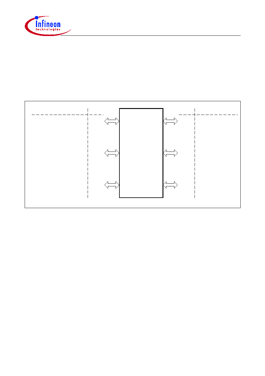
The TC11IB has 96 digital input/output port lines, which are organized into six parallel
16-bit ports, Port P0 to Port P5 with 3.3V nominal voltage.
The digital parallel ports can be all used as general purpose I/O lines or they can perform
input/output functions for the on-chip peripheral units. An overview on the port-to-
peripheral unit assignment is shown in
Figure 4
.
Figure 4
Parallel Ports of the TC11IB
M C A 0 49 51
TC 11IB
P a ra lle l P o rts
G P IO 3
G P IO 4
G P IO 5
G P IO
A lte rn a te F u n ctio n s
E xte rn a l In te rru p ts
E xte rn a l In te rru p ts
M M C I
G P IO 1
G P IO 0
G P IO 2
G P IO
A lte rn a te F u n ctio n s
E th e rn e t / M M C I
A S C / S S C / M M C I / 1 6 x5 0
G P T U 0 / G P T U 1
TC11IB
Data Sheet
26
V2.3, 2003-11
Serial Interfaces
The TC11IB includes three serial peripheral interface units:
� Asynchronous/Synchronous Serial Interface (ASC)
� High-Speed Synchronous Serial Interface (SSC)
� Asynchronous Serial Interface (16X50)
Asynchronous/Synchronous Serial Interface
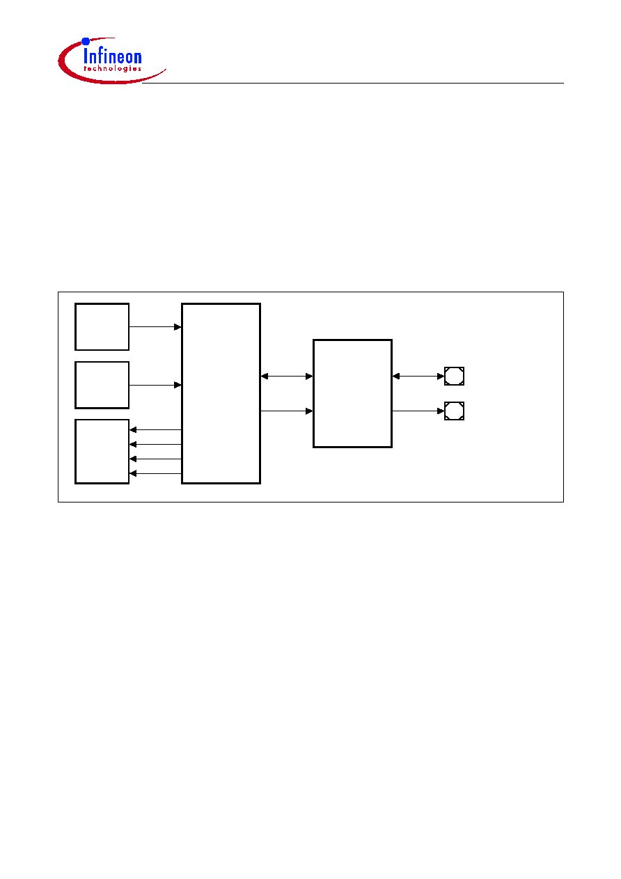
Figure 5
shows a global view of the functional blocks of the Asynchronous/Synchronous
Serial interface ASC.
Figure 5
General Block Diagram of the ASC Interfaces
ASC Module communicates with the external world via one pair of I/O lines. The RXD
line is the receive data input signal (in Synchronous Mode also output). TXD is the
transmit output signal. Clock control, address decoding, and interrupt service request
control are managed outside the ASC Module kernel.
The Asynchronous/Synchronous Serial Interface provides serial communication
between the TC11IB and other microcontrollers, microprocessors or external
peripherals.
The ASC supports full-duplex asynchronous communication and half-duplex
synchronous communication. In Synchronous Mode, data is transmitted or received
synchronous to a shift clock which is generated by the ASC internally. In Asynchronous
Mode, 8-bit or 9-bit data transfer, parity generation, and the number of stop bits can be
selected. Parity, framing, and overrun error detection are provided to increase the
reliability of data transfers. Transmission and reception of data are double-buffered. For
multiprocessor communication, a mechanism is included to distinguish address bytes
from data bytes. Testing is supported by a loop-back option. A 13-bit baud rate generator
M C B 0 4 9 3 8
C lo c k
C o n tro l
A d d re s s
D e c o d e r
In te rru p t
C o n tro l
f
A S C
A S C
M o d u le
P o rt
C o n tro l
P 1 .6 /
A S C _ R x D
R x D
T x D
P 1 .7 / A S C _ T x D

TC11IB
Data Sheet
27
V2.3, 2003-11
provides the ASC with a separate serial clock signal that can be very accurately adjusted
by a prescaler implemented as a fractional divider.
Features:
� Full duplex asynchronous operating modes
� 8- or 9-bit data frames, LSB first
� Parity bit generation/checking
� One or two stop bits
� Baudrate from 3 MBaud to 0.71 Baud (@ 48 MHz clock)
� Multiprocessor mode for automatic address/data byte detection
� Loop-back capability
� Support for IrDA data transmission up to 115.2 KBaud maximum
� Half-duplex 8-bit synchronous operating mode
� Baudrate from 6 MBaud to 488.3 Baud (@ 48 MHz clock)
� Double buffered transmitter/receiver
� Interrupt generation
� On a transmitter buffer empty condition
� On a transmit last bit of a frame condition
� On a receiver buffer full condition
� On an error condition (frame, parity, overrun error)
� FIFO
� 8 bytes receive FIFO (RXFIFO)
� 8 bytes transmit FIFO (TXFIFO)
� Independent control of RXFIFO and TXFIFO
� 9-bit FIFO data width
� Programmable Receive/Transmit Interrupt Trigger Level
� Receive and transmit FIFO filling level indication
� Overrun error generation
� Two pin pair RXD/TXD available at Port 1

TC11IB
Data Sheet
28
V2.3, 2003-11
High-Speed Synchronous Serial Interface
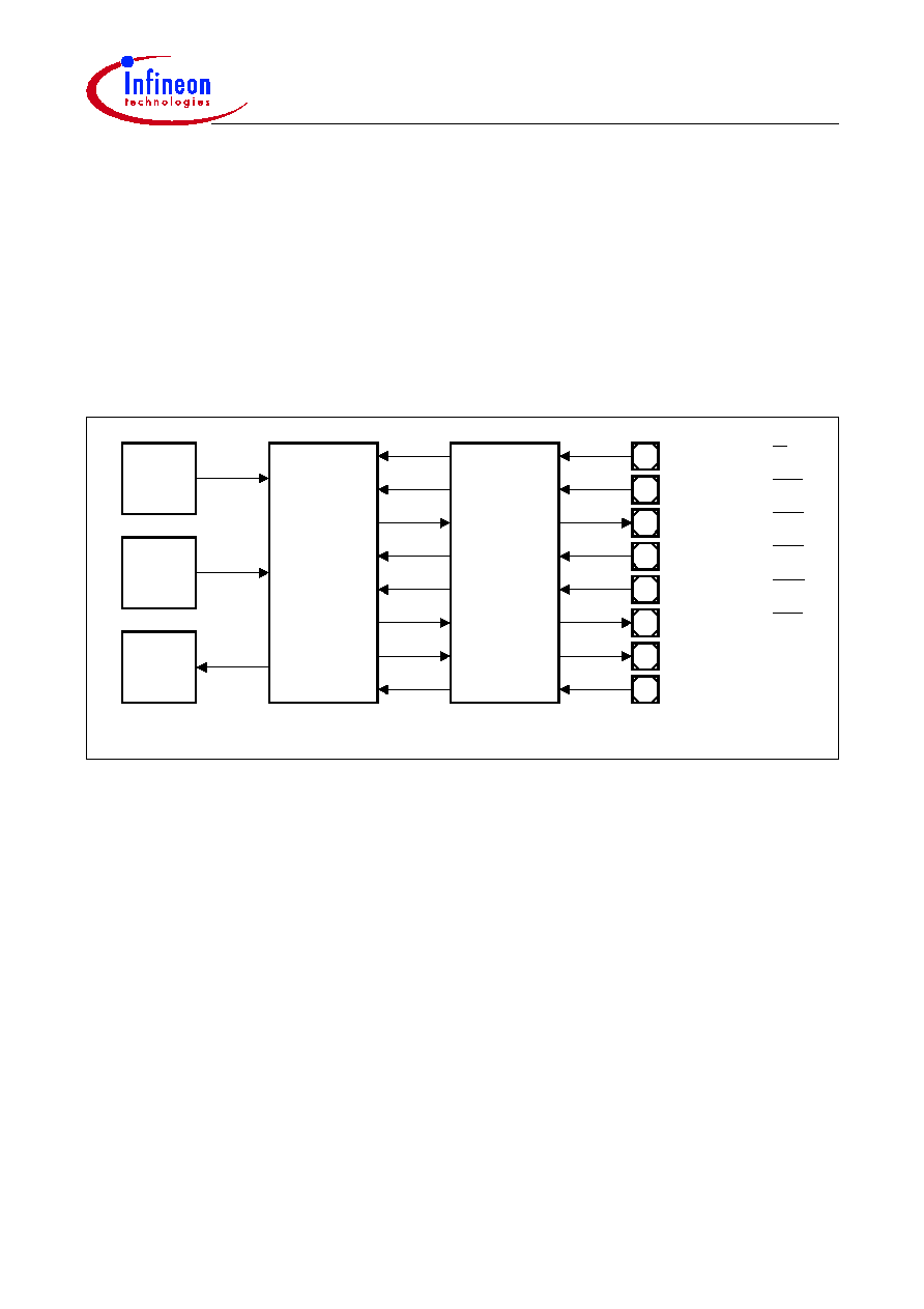
Figure 6
shows a global view of the functional blocks of the High-Speed Synchronous
Serial interface SSC.
Figure 6
General Block Diagram of the SSC Interfaces
The SSC Module has three I/O lines, located at Port 1. The SSC Module is further
supplied by separate clock control, interrupt control, address decoding, and port control
logic.
The SSC supports full-duplex and half-duplex serial synchronous communication up to
24 MBaud (@ 48 MHz module clock). The serial clock signal can be generated by the
SSC itself (master mode) or can be received from an external master (slave mode). Data
width, shift direction, clock polarity, and phase are programmable. This allows
communication with SPI-compatible devices. Transmission and reception of data are
double-buffered. A 16-bit baud rate generator provides the SSC with a separate serial
clock signal.
M C B 0 4 9 5 2
C lo c k
C o n tro l
A d d re s s
D e c o d e r
In te rru p t
C o n tro l
f
S S C
S S C
M o d u le
P o rt
C o n tro l
P 1 .2 / M T S R
T x D
R x D
T x D
R x D
M a s te r
S la v e
Slav
e
S
C
LK
M
a
st
er
P 1 .1 / M R S T
P 1 .0 / S C L K

TC11IB
Data Sheet
29
V2.3, 2003-11
Features:
� Master and slave mode operation
� Full-duplex or half-duplex operation
� Flexible data format
� Programmable number of data bits: 2 to 16 bit
� Programmable shift direction: LSB or MSB shift first
� Programmable clock polarity: idle low or high state for the shift clock
� Programmable clock/data phase: data shift with leading or trailing edge of the shift
clock
� Baud rate generation from 24 MBaud to 366.2 Baud (@ 48 MHz module clock)
� Interrupt generation
� On a transmitter empty condition
� On a receiver full condition
� On an error condition (receive, phase, baud rate, transmit error)
� Three-pin interface
� Flexible SSC pin configuration
TC11IB
Data Sheet
30
V2.3, 2003-11
Asynchronous Serial Interface (16X50)
The 16X50 is a universal asynchronous receiver/transmitter (UART) which is fully
prorammable.It supports word lengths from five to eight bits, an optional parity bit and
one or two stop bits.If enabled, the parity can be odd, even or forced to a defined state.
The 16X50 includes a 16-bit programmable baud rate generator and an 8-bit scratch
register, together with two 16-byte FIFOs -one for transmit and one for receive. It has six
modem control lines and supports a diagnostic loop-back mode. An interrupt can be
generated from any one of 10 sources.
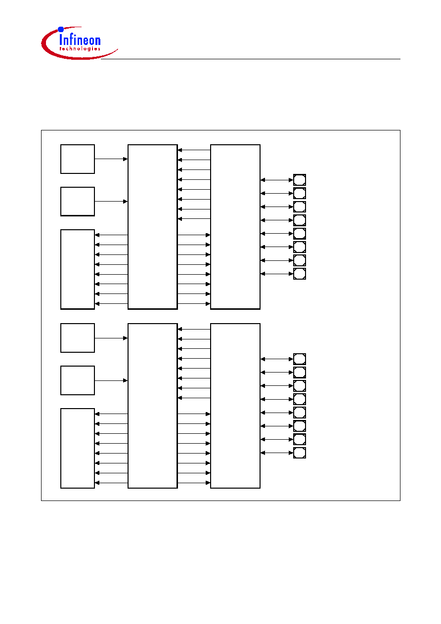
Figure 7
shows a global view of the functional
blocks of the Asynchronous Serial Interface (16X50).
Figure 7
General Block Diagram of the 16X50 Interface
The 16X50 Module communicates with the external world via five input and three output
lines located at Port 1.
The 16X50 provides serial asynchronous receive data synchronization, parallel-to-serial
and serial-to-parallel data conversions for both the transmitter and receiver sections.
These functions are necessary for converting the serial data stream into parallel data
that is required with digital data systems. Synchronization for the serial data stream is
accomplished by adding start and stops bits to the transmit data to form a data character
(character orientated protocol). Data integrity is insured by attaching a parity bit to the
data character. The parity bit is checked by the receiver for any transmission bit errors.
The electronic circuitry to provide all these functions is fairly complex especially when
manufactured on a single integrated silicon chip. The 16X50 represents such an
integration with greatly enhanced features.
The 16X50 is an upward solution that provides 16 bytes of transmit and receive FIFO
memory, instead of 1 byte provided in the 16C450. The 16X50 is designed to work with
high speed modems and shared network environments, that require fast data processing
time. Increased performance is realized in the 16X50 by the larger transmit and receive
M C B 0 4 9 3 7
C lo c k
C o n tro l
A d d re s s
D e c o d e r
In te rru p t
C o n tro l
f
1 6 x5 0
1 6 x 5 0
M o d u le
P o rt
C o n tro l
P 1 .1 5 / 1 6 x 5 0 _ R I
P 1 .1 4 / 1 6 x 5 0 _ C T S
P 1 .1 3 / 1 6 x 5 0 _ D T R
P 1 .1 2 / 1 6 x 5 0 _ D S R
P 1 .1 1 / 1 6 x 5 0 _ D C D
P 1 .1 0 / 1 6 x 5 0 _ R T S
P 1 .9 / 1 6 x 5 0 _ T x D
P 1 .8 / 1 6 x 5 0 _ R x D

TC11IB
Data Sheet
31
V2.3, 2003-11
FIFO's. This allows the external processor to handle more networking tasks within a
given time. The 4 selectable levels of FIFO trigger provided for maximum data
throughput performance especially when operating in a multi-channel environment. The
combination of the above greatly reduces the bandwidth requirement of the external
controlling CPU, increases performance, and reduces power consumption.
The 16X50 is capable of operation to 3 Mbps with a 48 MHz clock input (
f
16X50
).
Features:
� Software upward compatible with the NS16550A
� Standard modem interface
� Programmable word length, stop bits and parity
� Programmable baud rate generator
� Interrupt generation
� Diagnostic loop-back mode
� Scratch register
� Automatic hardware/software flow control
� Programmable XON/XOFF characters
� Independent transmit and receive control
� FIFO
� 16 byte transmit FIFO
� 16 byte receive FIFO with error flags
� Four selectable receive FIFO interrupt trigger levels
TC11IB
Data Sheet
32
V2.3, 2003-11
General Purpose Timer Units
Figure 8
shows a global view of all functional blocks of the two General Purpose Timer
Unit (GPTU0 & GPTU1) Modules.
Figure 8
General Block Diagram of the GPTU Interface
Each GPTU module, GPTU0 and GPTU1, consists of three 32-bit timers designed to
solve such application tasks as event timing, event counting, and event recording. And
each GPTU module communicates with the external world via eight I/O lines located at
Port 1.
M C B 0 4 9 4 3
C lo c k
C o n tro l
A d d re s s
D e c o d e r
In te rru p t
C o n tro l
f
G P T U 0
G P T U 0
M o d u le
P o rt
C o n tro l
P 0 .0 / G P T U 0 _ IO 0
P 0 .1 / G P T U 0 _ IO 1
P 0 .2 / G P T U 0 _ IO 2
P 0 .3 / G P T U 0 _ IO 3
P 0 .4 / G P T U 0 _ IO 4
P 0 .5 / G P T U 0 _ IO 5
P 0 .6 / G P T U 0 _ IO 6
P 0 .7 / G P T U 0 _ IO 7
S R 0
S R 1
S R 2
S R 3
S R 4
S R 5
S R 6
S R 7
IN 0
IN 1
IN 2
IN 3
IN 4
IN 5
IN 6
IN 7
O U T 0
O U T 1
O U T 2
O U T 3
O U T 4
O U T 5
O U T 6
O U T 7
C lo c k
C o n tro l
A d d re s s
D e c o d e r
In te rru p t
C o n tro l
f
G P T U 1
G P T U 1
M o d u le
P o rt
C o n tro l
P 0 .8 / G P T U 1 _ IO 0
P 0 .9 / G P T U 1 _ IO 1
P 0 .1 0 / G P T U 1 _ IO 2
P 0 .1 1 / G P T U 1 _ IO 3
P 0 .1 2 / G P T U 1 _ IO 4
P 0 .1 3 / G P T U 1 _ IO 5
P 0 .1 4 / G P T U 1 _ IO 6
P 0 .1 5 / G P T U 1 _ IO 7
S R 0
S R 1
S R 2
S R 3
S R 4
S R 5
S R 6
S R 7
IN 0
IN 1
IN 2
IN 3
IN 4
IN 5
IN 6
IN 7
O U T 0
O U T 1
O U T 2
O U T 3
O U T 4
O U T 5
O U T 6
O U T 7

TC11IB
Data Sheet
33
V2.3, 2003-11
The three timers in each GPTU Module T0, T1, and T2, can operate independently from
each other or can be combined:
General Features:
� All timers are 32-bit precision timers with a maximum input frequency of
f
GPTU
.
� Events generated in T0 or T1 can be used to trigger actions in T2
� Timer overflow or underflow in T2 can be used to clock either T0 or T1
� T0 and T1 can be concatenated to form one 64-bit timer
Features of T0 and T1:
� Each timer has a dedicated 32-bit reload register with automatic reload on overflow
� Timers can be split into individual 8-, 16-, or 24-bit timers with individual reload
registers
� Overflow signals can be selected to generate service requests, pin output signals, and
T2 trigger events
� Two input pins can determine a count option
Features of T2:
� Count up or down is selectable
� Operating modes:
� Timer
� Counter
� Quadrature counter (incremental/phase encoded counter interface)
� Options:
� External start/stop, one-shot operation, timer clear on external event
� Count direction control through software or an external event
� Two 32-bit reload/capture registers
� Reload modes:
� Reload on overflow or underflow
� Reload on external event: positive transition, negative transition, or both transitions
� Capture modes:
� Capture on external event: positive transition, negative transition, or both
transitions
� Capture and clear timer on external event: positive transition, negative transition, or
both transitions
� Can be split into two 16-bit counter/timers
� Timer count, reload, capture, and trigger functions can be assigned to input pins. T0
and T1 overflow events can also be assigned to these functions.
� Overflow and underflow signals can be used to trigger T0 and/or T1 and to toggle
output pins
� T2 events are freely assignable to the service request nodes.
TC11IB
Data Sheet
34
V2.3, 2003-11
MultiMediaCard Interface (MMCI)
The MultiMediaCard Interface module provides interface to MultiMediaCard bus. It
supports the full MultiMediaCard bus protocol as defined in MultiMediaCard system
specification version 1.3.
Figure 9
shows a global view of the MMCI module with the
module specific interface connections.
Figure 9
General Block Diagram of MMCI Interface
The MMCI module communicates with external world via two IO lines and five output
lines which are located at Port 1, 2 and 5. Clock control, interrupt service and address
decoding are managed outside the MMCI module Kernel.
MMCI handles the data transfer on CMD and DAT of the MMC Bus. It performs the
transfer from bit serial to byte parallel or vice versa and sustains a 16Mbps data rate. To
fulfil the MMC Bus protocol, special bytes are modified via inserting start and stop bits or
CRC bits. A clock controller is implemented to divide the clock to the necessary MMC
Bus clock frequency.
Features
� 3 line serial interface --- Glueless interface to MultiMediaCard Bus
� Pointer based data transfer
� Block and sequential card access
� 16MHz MultiMediaCard bus clock generation
� CRC protection for the MultiMediaCard bus communication
� Optional programming voltage control
� Buffered data transfer
� Power management
� Data communication with a data rate up to 2 Mbyte/s
M C B 0 4 9 4 6
C lo ck
C o n tro l
A d d re ss
D e co d e r
In te rru p t
C o n tro l
f
M M C I
M M C I
M o d u le
P o rt
C o n tro l
P 5 .1 5 / M M C I_ R O D
P 5 .2 / M M C I_ C M D _ R W
P 5 .0 / M M C I_ D A T _ R W
P 2 .7 / M M C I_ V D D E N
P 1 .5 / M M C I_ D A T
P 1 .4 / M M C I_ C M D
P 1 .3 / M M C I_ C L K
TC11IB
Data Sheet
35
V2.3, 2003-11
Ethernet Controller
The MAC controller implements the IEEE 802.3 and operates either at 100 Mbps or 10
Mbps.
Figure 10
shows a global view of the Ethernet Controller module with the module
specific interface connections.
Figure 10
General Block Diagram of the Ethernet Controller
The Ethernet controller comprises the following functional blocks:
1. Media Access Controller (MAC)
2. Receive Buffer (RB)
3. Transmit Buffer (TB)
4. Data Management Unit in Receive Direction (DMUR)
5. Data Management Unit in Transmit Direction (DMUT)
M C B 0 4 9 4 2
P o rt
C o n tro l
P 2 .1 5 / M II_ R x E R
F A S T
F P I
(M /S )
P 2 .1 4 /
M II_ R x D [3 ]
P 2 .1 3 /
M II_ R x D [2 ]
P 2 .1 2 /
M II_ R x D [1 ]
P 2 .1 1 /
M II_ R x D [0 ]
P 2 .1 0 / M II_ C O L
P 2 .9 / M II_ C R S
P 2 .8 / M II_ R x D V
P 2 .6 / M II_ M D C
P 2 .5 / M II_ T x E N
P 2 .4 / M II_ T x E R
P 2 .3 / M II_ T x D [3 ]
P 2 .2 / M II_ T x D [2 ]
P 2 .1 / M II_ T x D [1 ]
P 2 .0 / M II_ T x D [0 ]
M II_ T x C L K
M II_ T x C L K
M II_ T D IO
M II
M A C
E th e rn e t
C o n tro lle r
R B
T B
D M U R
D M U T

TC11IB
Data Sheet
36
V2.3, 2003-11
RB as well as TB provides on-chip data buffering whereas DMUR and DMUT perform
data transfer from/to the shared memory.
Two interfaces are provided by the Ethernet Controller Module:
1. MII interface for connection of Ethernet PHYs via eighteen Input / Output lines
2. Master/slave FPI bus interface for connection to the on-chip system bus for data
transfer as well as configuration.
Features
� Media Independent Interface (MII) according to IEEE 802.3
� Support 10 or 100 Mbps MII-based Physical devices.
� Support Full Duplex Ethernet.
� Support data transfer between Ethernet Controller and COM-DRAM.
� Support data transfer between Ethernet Controller and SDRAM via EBU.
� 256 x 32 bit Receive buffer and Transmit buffer each.
� Support burst transfers up to 8 x 32 Byte.
Media Access Controller (MAC)
� 100/10-Mbps operations
� Full IEEE 802.3 compliance
� Station management signaling
� Large on-chip CAM (Content Addressable Memory)
� Full duplex mode
� 80-byte transmit FIFO
� 16-byte receive FIFO
� PAUSE Operation
� Flexible MAC Control Support
� Support Long Packet Mode and Short Packet Mode
� PAD generation
Media Independent Interface (MII)
� Media independence.
� Multi-vendor point of interoperability.
� Support connection of MAC layer and Physical (PHY) layer devices.
� Capable of supporting both 100 Mb/s and 10 Mb/s data rates.
� Data and delimiters are synchronous to clock references.
� Provides independent four bit wide transmit and receive data paths.
� Support connection of PHY layer and Station Management (STA) devices.
� Provides a simple management interface.
� Capable of driving a limited length of shielded cable.
TC11IB
Data Sheet
37
V2.3, 2003-11
PCI
The PCI Interface module of the TC11IB basically is a bus bridge between the on-chip
FPI bus and the external PCI bus of the system. The PCI Interface is fully compliant to
PCI Local Bus Specification Rev. 2.2.
Figure 11
shows a global view of the PCI module
with the module specific pin connections.
Figure 11
General Block Diagram of the PCI Interface
The PCI-FPI bridge is able to execute a number of various data transfers between the
FPI bus and the PCI bus. Beside the standard PCI functions (configuration transactions),
there are two main types of transfers which the bridge supports. Firstly, it will forward a
transaction that any PCI initiator directs to the PCI interface of the TC11IB to the on-chip
FPI bus. Secondly the bridge will forward certain transactions that a FPI master initiates
on the FPI bus to the PCI bus. Depending on configuration, these transfers may be a
M C B 0 4 9 4 9
P C I
M o d u le
P _ A D [3 1 :0 ]
P _ C /B E [3 :0 ]
P _ P A R
P _ S E R R
P _ P E R R
P _ S T O P
P _ D E V S E L
P _ T R D Y
P _ F R A M E
P _ IR D Y
P _ L O C K
P _ IN T A
P _ IN T B
P _ P M E
P _ R E Q
P _ G N T
P _ ID S E L
P _ C L K 3 3
F A S T
F P I
(M /S )

TC11IB
Data Sheet
38
V2.3, 2003-11
single data or burst transfers on both PCI and FPI bus. In addition, the bridge is able to
handle a direct data transfer between PCI bus and FPI bus utilizing it's programmable
DMA channel. The DMA channel can only be activated by a FPI master. In order to work
as a PCI host bridge on the PCI bus, the variety of PCI transactions issued by the bridge
includes configuration transactions of type 0 and type 1 when acting as a PCI master.
Features
� PCI V2.2 compliant, 32 bit, 33 MHz
� Multifunction Device, Support both PCI Master/Host functions. These functions can be
activated by:
� TriCore
� Fast Ethernet
� DMA Channel
� Support Burst Transfer from PCI to ComDRAM, SDRAM and LMU.
� Support DMA Channel data transfers between PCI and FPI
� Loading of PCI Configuration Registers done by TriCore via FPI Bus access
� Support PCI Command
� Support Card-Bus.
� Power management
� according to PCI Bus Power Management Interface Specification V1.1
� Support Multiple PCI power management states D0, D1, D2, D3
cold
� PME#-Signalling from Fast Ethernet in D1, D2.
� PCI Reset
� All tristatable PCI outputs of the bridge are set to "Tristate" upon PCI Reset,
compliant to PCI Local Bus Specification V2.2

TC11IB
Data Sheet
39
V2.3, 2003-11
On-Chip Memories
The TC11IB provides the following on-chip memories:
� Program Memory Unit (PMU) with
� 24 KBytes Scratch-pad Code RAM (SRAM)
� 8 KBytes Instruction Cache Memory (I-CACHE)
� Data Memory Unit (DMU) with
� 24 KBytes Scratch-pad Data RAM (SRAM)
� 8 KBytes Data Cache Memory (D-CACHE)
� 16 KBytes Boot ROM (BROM)
� eDRAM Local Memory Unit (LMU) with
� 512 KBytes Code/Data Memory
� ComDRAM with
� 1MBytes Code/Data Memory
� Peripheral Control Processor (PCP) with
� 16 KBytes Data Memory (PCODE)
� 4 KBytes Parameter RAM (PRAM)
TC11IB
Data Sheet
40
V2.3, 2003-11
Address Map
Table 2
defines the specific segment oriented address blocks of the TC11IB with its
address range, size, and PMU/DMU access view.
Table 3
shows the block address map
of the Segment 15 which includes on-chip peripheral units and ports.
Table 2
TC11IB Block Address Map
Seg-
ment
Address
Range
Size
Description
DMU
Acc.
PMU
Acc.
0 � 7 0000 0000
H
�
7FFF FFFF
H
2 GB
MMU/ FPI Space
via
F_FPI
via
F_ FPI
c
a
c
h
e
d
8
8000 0000
H
�
8FFF FFFF
H
256 MB
External Memory Space
mapped from Segment 10
via
LMB
via
LMB
9
9000 0000
H
�
9FDF FFFF
H
254 MB
PCI Space
mapped from Segment 11
via
F_FPI
via
F_FPI
9FE0 0000
H
�
9FEF FFFF
H
1 MB
ComDRAM Space
mapped from Segment 11
9FF0 0000
H
�
9FFF FFFF
H
1 MB
Reserved
�
�
10
A000 0000
H
�
AFBF FFFF
H
252 MB
External Memory Space
via
LMB
via
LMB
n
o
n-
c
a
c
h
e
d
AFC0 0000
H
�
AFC7 FFFF
H
512 KB
LMU Space
via
LMB
via
LMB
AFC8 0000
H
�
AFFF FFFF
H
3.5 MB
Reserved
�
�
11
B000 0000
H
�
BFDF FFFF
H
254 MB
PCI Space
mappable into segment 9
via
F_FPI
via
F_FPI
BFE0 0000
H
�
BFEF FFFF
H
1 MB
ComDRAM Space
BFF0 0000
H
�
BFFF FFFF
H
1 MB
Reserved
�
�
12
C000 0000
H
�
C007 FFFF
H
512 KB
Local Memory Unit eDRAM
Space
via
LMB
via
LMB
c
a
c
h
e
d
C008 0000
H
�
CFFF FFFF
H
255.5
MB
Reserved
�
�

TC11IB
Data Sheet
41
V2.3, 2003-11
13
D000 0000
H
�
D000 5FFF
H
24 KB
Local Data Scratchpad Memory
(SRAM)
DMU
local
via
LMB
non-cached
D000 6000
H
�
D3FF FFFF
H
~ 64 MB Reserved
�
�
D400 0000
H
�
D400 5FFF
H
24 KB
Local Code Scratchpad
Memory (SRAM)
via
LMB
PMU
local
D400 6000
H
�
D7FF FFFF
H
~64 MB
Reserved
�
�
D800 0000
H
�
DDFF FFFF
H
96 MB
External Memory Space
via
LMB
via
LMB
DE00 0000
H
�
DEFF FFFF
H
16 MB
Emulator Memory Space
DF00 0000
H
�
DFFF BFFF
H
~16 MB
Reserved
�
�
DFFF C000
H
�
DFFF FFFF
H
16 KB
Boot ROM Space
via
S_FPI
via
S_FPI
14
E000 0000
H
�
E7FF FFFF
H
128 MB
External Memory Space
via
LMB
�
E800 0000
H
�
E807 FFFF
H
512 KB
Local Memory Space
mapped to LMB Segment 12
�
E808 0000
H
�
E83F FFFF
H
3.5 MB
Reserved
E840 0000
H
�
E840 7FFF
H
32 KB
Local Data Memory (SRAM)
mapped to LMB Segment 13
E840 8000
H
�
E84F FFFF
H
~1 MB
Reserved
E850 0000
H
�
E850 7FFF
H
32 KB
Local Code Memory (SRAM)
mapped to LMB Segment 13
E850 8000
H
�
EFFF FFFF
H
~123
MB
Reserved
Table 2
TC11IB Block Address Map(cont'd)
Seg-
ment
Address
Range
Size
Description
DMU
Acc.
PMU
Acc.

TC11IB
Data Sheet
42
V2.3, 2003-11
Note: Accesses to address defined as "Reserved" in
Table 2
lead to a bus error. The
exceptions are marked with
1)
15
F000 0000
H
�
F00F FFFF
H
1 MB
On-Chip Peripherals & Ports
via
S_FPI
via
S_FPI
non-c
a
ched
F010 0000
H
�
F017 FFFF
H
1)
512 KB
Reserved
�
�
F018 0000
H
�
F018 FFFF
H
64 KB
ComDRAM Control Registers
via
S_FPI
via
S_FPI
F019 0000
H
�
F03F FFFF
H
1)
2.4375
MB
Reserved
�
�
F040 0000
H
�
F04F FFFF
H
1 MB
PCI/FPI-Bridge Registers
via
F_FPI
�
F050 0000
H
�
F0FF FFFF
H
~11 MB
Reserved
�
F100 0000
H
�
F1FF FFFF
H
16 MB
PCI Configuration Space
via
F_FPI
F200 0000
H
�
F200 05FF
H
6 x 256
B
BCU0 and Fast Ethernet
Registers
F200 0600
H
�
F7E0 FEFF
H
~94 MB
Reserved
�
F7E0 FF00
H
�
F7E0 FFFF
H
256 B
CPU Slave Interface Registers
(CPS)
via
F_FPI
F7E1 0000
H
�
F7E1 FFFF
H
64 KB
Core SFRs
F7E2 0000
H
�
F7FF FFFF
H
15 x 128
KB
Reserved
�
F800 0000
H
�
F87F FFFF
H
8 MB
LMB Peripheral Space
(EBU_LMB and local memory
eDRAM control registers)
via
LMB
F880 0000
H
�
FFFF FFFF
H
120 MB
Reserved
�
1)
Any access to this area will result in unpredicted behaviors of PORTs.
Table 2
TC11IB Block Address Map(cont'd)
Seg-
ment
Address
Range
Size
Description
DMU
Acc.
PMU
Acc.

TC11IB
Data Sheet
43
V2.3, 2003-11
Table 3
Block Address Map of Segment 15
Symbol Description
Address Range
Size
SCU
System Control Unit F000
0000
H
� F000 00FF
H
256 Bytes
PCISIR
PCI Software Interrupt Request
F000 0100
H
� F000 01FF
H
256 Bytes
BCU1
Slow FPI Bus Control Unit 1
F000 0200
H
� F000 02FF
H
256 Bytes
STM
System Timer
F000 0300
H
� F000 03FF
H
256 Bytes
OCDS
On-Chip Debug Support
F000 0400
H
� F000 04FF
H
256 Bytes
�
Reserved
F000 0500
H
� F000 05FF
H
�
GPTU0
General Purpose Timer Unit 0
F000 0600
H
� F000 06FF
H
256 Bytes
GPTU1
General Purpose Timer Unit 1
F000 0700
H
� F000 07FF
H
256 Bytes
ASC
Async./Sync. Serial Interface
F000 0800
H
� F000 08FF
H
256 Bytes
16X50
Asynchronous Serial Interface
F000 0900
H
� F000 09FF
H
256 Bytes
SSC
High-Speed Synchronous Serial
Interface
F000 0A00
H
� F000 0AFF
H
256 Bytes
MMCI
MultiMediaCard Interface
F000 0B00
H
� F000 0BFF
H
256 Bytes
SRU
Service Request Unit
F000 0C00
H
� F000 0DFF
H
512 Bytes
�
Reserved
F000 0E00
H
� F000 27FF
H
�
P0
Port 0
F000 2800
H
� F000 28FF
H
256 Bytes
P1
Port 1
F000 2900
H
� F000 29FF
H
256 Bytes
P2
Port 2
F000 2A00
H
� F000 2AFF
H
256 Bytes
P3
Port 3
F000 2B00
H
� F000 2BFF
H
256 Bytes
P4
Port 4
F000 2C00
H
� F000 2CFF
H
256 Bytes
P5
Port 5
F000 2D00
H
� F000 2DFF
H
256 Bytes
�
Reserved
F000 2E00
H
� F000 3EFF
H
�
PCP
PCP Registers
F000 3F00
H
� F000 3FFF
H
256 Bytes
Reserved
F000 4000
H
� F000 FFFF
H
�
PCP Data Memory (PRAM)
F001 0000
H
� F001 0FFF
H
4 KBytes
Reserved
F001 1000
H
� F001 FFFF
H
�
PCP Code Memory (PCODE)
F002 0000
H
� F002 3FFF
H
16 KBytes
�
Reserved
F002 4000
H
� F017 FFFF
H
�
1)
Com-
DRAM
ComDRAM Control Registers
F018 0000
H
� F018 FFFF
H
64 KBytes
�
Reserved
F019 0000
H
� F03F FFFF
H
�
1)

TC11IB
Data Sheet
44
V2.3, 2003-11
PCI
PCI Bridge Configuration
Registers
F040 0000
H
� F04F FFFF
H
1 MBytes
�
Reserved
F050 0000
H
� F0FF FFFF
H
�
PCI_CS
x(x=1,2)
PCI Configuration Space
Registers
F100 0000
H
� F1FF FFFF
H
16 MBytes
BCU0
Fast FPI Bus Control Unit 0
F200 0000
H
� F200 00FF
H
256 Bytes
ECU
Ethernet Controller Unit
F200 0100
H
� F200 05FF
H
1280 Bytes
�
Reserved
F200 0600
H
� F7E0 FEFF
H
�
CPU
Slave Interface Registers (CPS) F7E0 FF00
H
� F7E0 FFFF
H
256 Bytes
Reserved
F7E1 0000
H
� F7E1 7FFF
H
�
MMU
F7E1 8000
H
� F7E1 80FF
H
256 BYTES
Reserved
F7E1 8100
H
� F7E1 BFFF
H
�
Memory Protection Registers
F7E1 C000
H
� F7E1 EFFF
H
12 KBytes
Reserved
F7E1 F000
H
� F7E1 FCFF
H
�
Core Debug Register (OCDS)
F7E1 FD00
H
� F7E1 FDFF
H
256 Bytes
Core Special Function Registers
(CSFRs)
F7E1 FE00
H
� F7E1 FEFF
H
256 Bytes
General Purpose Register
(GPRs)
F7E1 FF00
H
� F7E1 FFFF
H
256 Bytes
�
Reserved
F7E2 0000
H
� F7FF FFFF
H
�
EBU
EBU_LMB External Bus Unit
F800 0000
H
� F800 01FF
H
512 Bytes
�
Reserved
F800 0200
H
� F800 03FF
H
�
LMU
Local Memory Unit
F800 0400
H
� F800 04FF
H
256 Bytes
�
Reserved
F800 0500
H
� F87F FBFF
H
�
DMU
Local Data Memory Unit
F87F FC00
H
� F87F FCFF
H
256 Bytes
PMU
Local Program Memory Unit
F87F FD00
H
� F87F FDFF
H
256 Bytes
LCU
LMB Bus Control Unit
F87F FE00
H
� F87F FEFF
H
256 Bytes
LFI
LMB to FPI Bus Bridge (LFI)
F87F FF00
H
� F87F FFFF
H
256 Bytes
�
Reserved
F880 0000
H
� FFFF FFFF
H
�
1)
Any access to this area will result in unpredicted behaviors of PORTs.
Table 3
Block Address Map of Segment 15(cont'd)
Symbol Description
Address Range
Size

TC11IB
Data Sheet
45
V2.3, 2003-11
Note: Accesses to address defined as "Reserved" in
Table 3
lead to a bus error.The
exceptions are marked with
1)
Memory Protection System
The TC11IB memory protection system specifies the addressable range and read/write
permissions of memory segments available to the currently executing task. The memory
protection system controls the position and range of addressable segments in memory.
It also controls the kinds of read and write operations allowed within addressable
memory segments. Any illegal memory access is detected by the memory protection
hardware, which then invokes the appropriate Trap Service Routine (TSR) to handle the
error. Thus, the memory protection system protects critical system functions against both
software and hardware errors. The memory protection hardware can also generate
signals to the Debug Unit to facilitate tracing illegal memory accesses.
In SAF-T11IB-64D96, TriCore supports two address spaces: The virtual address space
and The physical address space. Both address space are 4GB in size and divided into
16 segments with each segment being 256MB. The upper 4 bits of the 32-bit address are
used to identify the segment. Virtual segments are numbered 0 - 15. But a virtual address
is always translated into a physical address before accessing memory. The virtual
address is translated into a physical address using one of two translation mechanisms:
(a) direct translation, and (b) Page Table Entry (PTE) based translation. If the virtual
address belongs to the upper half of the virtual address space then the virtual address is
directly used as the physical address (direct translation). If the virtual address belongs to
the lower half of the address space, then the virtual address is used directly as the
physical address if the processor is operating in Physical mode (direct translation) or
translated using a Page Table Entry if the processor is operating in Virtual mode (PTE
translation). These are managed by Memory Management Unit (MMU)
Memory protection is enforced using separate mechanisms for the two translation paths.
Protection for direct translation
Memory protection for addresses that undergo direct translation is enforced using the
range based protection that has been used in the previous generation of the TriCore
architecture. The range based protection mechanism provides support for protecting
memory ranges from unauthorized read, write, or instruction fetch accesses. The
TriCore architecture provides up to four protection register sets with the PSW.PRS field
controlling the selection of the protection register set. Because the TC11IB uses a
Harvard-style memory architecture, each Memory Protection Register Set is broken
down into a Data Protection Register Set and a Code Protection Register Set. Each Data
Protection Register Set can specify up to four address ranges to receive particular
protection modes. Each Code Protection Register Set can specify up to two address
ranges to receive particular protection modes.

TC11IB
Data Sheet
46
V2.3, 2003-11
Each of the Data Protection Register Sets and Code Protection Register Sets
determines the range and protection modes for a separate memory area. Each contains
register pairs which determine the address range (the Data Segment Protection
Registers and Code Segment Protection Registers) and one register (Data Protection
Mode Register) which determines the memory access modes which apply to the
specified range.
Protection for PTE based translation
Memory protection for addresses that undergo PTE based translation is enforced using
the PTE used for the address translation. The PTE provides support for protecting a
process from unauthorized read, write, or instruction fetches by other processes. The
PTE has the following bits that are provided for the purpose of protection:
l XE (Execute Enable) enables instruction fetch to the page.
l WE (Write Enable) enables data writes to the page.
l RE (Read Enable) enables data reads from the page.
Furthermore, User-0 accesses to virtual addresses in the upper half of the virtual
address space are disallowed when operating in Virtual mode. In Physical mode, User-
0 accesses are disallowed only to segments 14 and 15. Any User-0 access to a virtual
address that is restricted to User-1 or Super-visor mode will cause a Virtual Address
Protection (VAP) Trap in both the Physical and Virtual modes.

TC11IB
Data Sheet
47
V2.3, 2003-11
On-Chip Bus System
The TC11IB includes two bus systems:
� Local Memory Bus (LMB)
� On-Chip FPI Bus (Fast FPI and Slow FPI)
There are two bridges to interconnect these three buses. The LMB-to-FPI (LFI)
interfaces the Fast FPI bus to LMB Bus. The FPI-to-FPI (FFI) interfaces slow FPI bus to
Fast FPI bus.
Local Memory Bus (LMB)
The Local Memory Bus interconnects the memory units and functional units, such as
CPU and LMU. The main target of the LMB bus is to support devices with fast response
times, optimized for speed. This allows the DMU and PMU fast access to local memory
and reduces load on the FPI bus. The Tricore system itself is located on LMB bus. Via
External Bus Unit, it interconnects TC11IB and external components.
The Local Memory Bus is a synchronous, pipelined, split bus with variable block size
transfer support. It supports 8,16,32 & 64 bits single beat transactions and variable
length 64 bits block transfers.
Key Features
The LMB provides the following features:
� Synchronous, Pipelined, Multi-master, 64-bit high performance bus
� Support multiple bus masters
� Support Split transactions
� Support Variable block size transfer
� Burst Mode Read/Write to Memories
� Connect Caches and on-chip memory and Fast FPI Bus

TC11IB
Data Sheet
48
V2.3, 2003-11
On-Chip FPI Bus
The FPI Bus interconnects the functional units of the TC11IB, such as the PCP and on-
chip peripheral components. The FPI Bus is designed to be quick to acquire by on-chip
functional units, and quick to transfer data. The low setup overhead of the FPI Bus
access protocol guarantees fast FPI Bus acquisition, which is required for time-critical
applications.The FPI Bus is designed to sustain high transfer rates. For example, a peak
transfer rate of up to 800 MBytes/s can be achieved with a 100 MHz bus clock and 32-
bit data bus. Multiple data transfers per bus arbitration cycle allow the FPI Bus to operate
at close to its peak bandwidth. Via External Bus Unit (EBU), FPI Bus also interconnects
the external components to TC11IB.
There are two FPI buses in TC11IB, Fast FPI Bus and Slow FPI Bus. In order to improve
the system performance, the peripherals are splitted into two FPI buses based on their
performance. The fast FPI bus runs at a speed of 96 MHz where most of the high
performance peripheral like ComDRAM, PCI-FPI, Ethernet Controller, LFI etc. are
connected. The slow FPI bus runs at half speed of its fast counter part. And it is used to
connect some standard peripherals. There is a FPI-FPI bridge between them to transfer
data. Each of FPI buses has its own Bus Control Unit (BCU).
Features
� Supports multiple bus masters
� Supports demultiplexed address/data operation
� Address bus up to 32 bits and data buses are 64 bits wide
� Data transfer types include 8-, 16-, 32- and 64 bit sizes
� Supports Burst transfer
� Single- and multiple-data transfers per bus acquisition cycle
� Designed to minimize EMI and power consumption
� Controlled by an Bus Control Unit (BCU)
� Arbitration of FPI Bus master requests
� Handling of bus error.
FFI-Bridge Features
� Supports Single/Block* Data Read/Write Transactions (8/16/32 Bit)
� Supports FPI- Read Modify Write Transactions (RMW)
� Internal FIFO Interfaces between FPI master and FPI slave.
� Optimized for FPI-Bus frequency ratios 2:1
� Special Retry/Abort functionality
Note: Block Transaction support depends on generic settings and the depth of the
bridge internal read- and write data buffer.

TC11IB
Data Sheet
49
V2.3, 2003-11
LFI
The LMB-to-FPI Interface (LFI) block provides the circuitry to interface (bridge) the FPI
bus to the Local Memory Bus (LMB).
LFI Features
� Compatible with the FPI 3.2 and LMB bus Specification V2.4
� Supports Burst/Single transactions, from FPI to LMB.
� Supports Burst/Single transactions, from LMB to FPI
� High efficiency and performance:
� fastest access across the bridge takes three cycles, using a bypass.
� There are no dead cycles on arbitration.
� Acts as the default master on FPI side.
� Supports abort, error and retry conditions on both sides of the bridge.
� Supports FPI's clock the same, or half, as the LMB's clock frequency.
� LMB clock is shut when no transactions are issue to LFI from both buses and none
are in process in the LFI to minimize the power consumption.

TC11IB
Data Sheet
50
V2.3, 2003-11
LMB External Bus Unit
The LMB External Bus Control Unit (EBU_LMB) of the TC11IB is the interface between
external resources, like memories and peripheral units, and the internal resources
connected to on-chip buses if enabled. The basic structure and external interconnections
of the EBU are shown in
Figure 12
.
Figure 12
EBU Structure and Interfaces
M C B 0 4 9 4 1
E B U _ L M B
A D [3 1 :0 ]
B C [3 :0 ]
A [2 3 :0 ]
R D
R D /W R
W A IT
S V M
H L D A
B R E Q
A L E
R A S
C S [6 :0 ]
C S E M U
C S G L B
C S O V L
C A S
C K E
M R /W
R M W
H O L D
C S F P I
E B U C L K
B A A
A D V
A C L K
C M D E L A Y
3 2
4
2 4
7
L M U
L M B
P M U
D M U
L F I
M M U
T riC o re
F A S T F P I
T o P e rip h e ra ls
F F I
T o P e rip h e ra ls
a n d P C P
S L O W F P I

TC11IB
Data Sheet
51
V2.3, 2003-11
The EBU is mainly used for the following two operations:
� Masters on LMB bus access external memories through EBU_LMB
� An external (off-chip) master access internal (on-chip) devices through FPI Bus.
The EBU controls all transactions required for these two operations and in particular
handles the arbitration of the external bus between multi-masters.
The types of external resources accessed by the EBU are:
� INTEL style peripherals (separate RD and WR signals)
� Motorola style peripherals (MR/ W signals)
� ROMs, EPROMs
� Static RAMs
� PC 100 SDRAMs (Burst Read/Write Capacity / Multi-Bank/Page support)
� Specific types of Burst Mode Flashes (Intel 28F800F3/28F160F3, AMD 29BL162)
� Special support for external emulator/debug hardware
Features
� Support Local Memory Bus (LMB 64-bit)
� Support External bus frequency up to 96 MHz and internal LMB frequency up to 166
MHz. External bus frequency: LMB frequency =1:1 or 1:2 or 1:4
� Highly programmable access parameters
� Support Intel-and Motorola-style peripherals/devices
� Support PC 100 SDRAM (burst access, multibanking, precharge, refresh)
� Support 16-and 32-bit SDRAM data bus and 64,128 and 256MBit devices
� Support Burst flash (Intel 28F800F3/160F3,AMD 29BL162)
� Support Multiplexed access (address &data on the same bus) when PC 100 SDRAM
is not implemented
� Support Address Alignment, external address space up to 64 MBytes.
� Support Data Buffering: Code Prefetch Buffer, Read/Write Buffer.
� External master arbitration compatible to C166 and other Tricore devices
� 8 programmable address regions (1 dedicated for emulator)
� Support Little-and Big-endian
� Signal for controlling data flow of slow-memory buffer
� Slave unit for external (off-chip) master to access devices on FPI bus

TC11IB
Data Sheet
52
V2.3, 2003-11
Peripheral Control Processor
The Peripheral Control Processor (PCP) performs tasks that would normally be
performed by the combination of a DMA controller and its supporting CPU interrupt
service routines in a traditional computer system. It could easily be considered as the
host processor's first line of defense as an interrupt-handling engine. The PCP can off-
load the CPU from having to service time-critical interrupts. This provides many benefits,
including:
� Avoiding large interrupt-driven task context-switching latencies in the host processor
� Lessening the cost of interrupts in terms of processor register and memory overhead
� Improving the responsiveness of interrupt service routines to data-capture and data-
transfer operations
� Easing the implementation of multitasking operating systems.
The PCP has an architecture which efficiently supports DMA type transactions to and
from arbitrary devices and memory addresses within the TC11IB and also has
reasonable stand alone computational capabilities.
The PCP is made up of several modular blocks as follows:
� PCP Processor Core
� Code Memory (PCODE)
� Parameter Memory (PRAM)
� PCP Interrupt Control Unit (PICU)
� PCP Service Request Nodes (PSRN)
� System bus interface to the slow FPI Bus
The PCP is fully interrupt-driven, meaning it is only activated through service requests;
there is no main program running in the background as with a conventional processor.
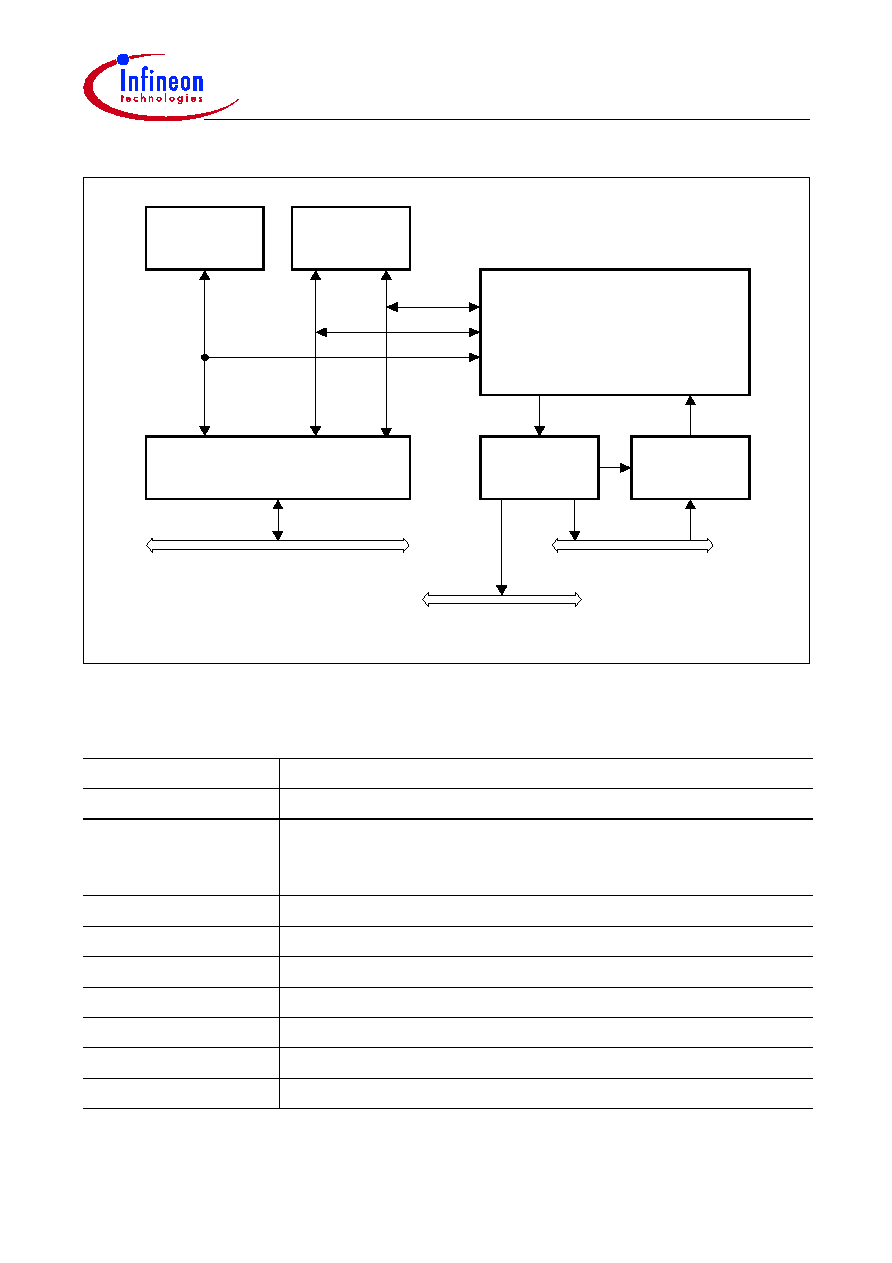
TC11IB
Data Sheet
53
V2.3, 2003-11
Figure 13
PCP Block Diagram
Table 4
PCP Instruction Set Overview
Instruction Group
Description
DMA primitives
Efficient DMA channel implementation
Load/Store
Transfer data between PRAM or FPI memory and the general
purpose registers, as well as move or exchange values
between registers
Arithmetic
Add, subtract, compare and complement
Divide/Multiply
Divide and multiply
Logical
And, Or, Exclusive Or, Negate, MCLR and MSET
Shift
Shift right or left, rotate right or left, prioritize
Bit Manipulation
Set, clear, insert and test bits
Flow Control
jump conditionally, jump long, exit, No operation
Miscellaneous
Debug
M C B 0 4 7 8 4
P C P
P ro c e s s o r
C o re
P C P S e rv ic e
R e q . N o d e s
P S R N s
P C P In te rru p t
C o n tro l U n it
P IC U
P a ra m e te r
M e m o ry
P R A M
C o d e
M e m o ry
P C O D E
F P I-In te rfa c e
P C P In te rru p t
A rb itra tio n B u s
C P U In te rru p t
A rb itra tio n B u s
F P I B u s
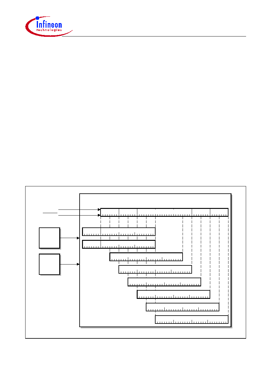
TC11IB
Data Sheet
54
V2.3, 2003-11
System Timer
The STM within the TC11IB is designed for global system timing applications requiring
both high precision and long range. The STM provides the following features:
� Free-running 56-bit counter
� All 56 bits can be read synchronously
� Different 32-bit portions of the 56-bit counter can be read synchronously
� Driven by clock,
f
STM
(identical with the system clock
f
SYS
= 48MHz).
� Counting begins at power-on reset
� Continuous operation is not affected by any reset condition except power-on reset
The STM is an upward counter, running with the system clock frequency. It is enabled
per default after reset, and immediately starts counting up. Other than via reset, it is no
possible to affect the contents of the timer during normal operation of the application, it
can only be read, but not written to. Depending on the implementation of the clock control
of the STM, the timer can optionally be disabled or suspended for power-saving and
debugging purposes via a clock control register.
The maximum clock period is 2
56
�
f
STM
. At
f
STM
= 48 MHz, for example, the STM
counts 47.6 years before overflowing. Thus, it is capable of continuously timing the entire
expected product life-time of a system without overflow.
Figure 14
Block Diagram of the STM Module
STM M odule
0 0
H
C A P
T IM 6
T IM 5
T IM 4
T IM 3
T IM 2
T IM 1
T IM 0
0 0
H
5 5
4 7
3 9
3 1
2 3
1 5
7
5 6 -B it S y s te m T im e r
A d d re s s
D e c o d e r
C lo c k
C o n tro l
E n a b le /
D is a b le
P O R S T
f
S T M
M C A 0 4 7 9 5

TC11IB
Data Sheet
55
V2.3, 2003-11
Watchdog Timer
The Watchdog Timer (WDT) provides a highly reliable and secure way to detect and
recover from software or hardware failure. The WDT helps to abort an accidental
malfunction of the TC11IB in a user-specified time period. When enabled, the WDT will
cause the TC11IB system to be reset if the WDT is not serviced within a user-
programmable time period. The CPU must service the WDT within this time interval to
prevent the WDT from causing a TC11IB system reset. Hence, routine service of the
WDT confirms that the system is functioning properly.
In addition to this standard "Watchdog" function, the WDT incorporates the EndInit
feature and monitors its modifications. A system-wide line is connected to the ENDINIT
bit implemented in a WDT control register, serving as an additional write-protection for
critical registers (besides Supervisor Mode protection).
A further enhancement in the TC11IB's Watchdog Timer is its reset prewarning
operation. Instead of immediately resetting the device on the detection of an error, as
known from standard Watchdogs, the WDT first issues an Non-maskable Interrupt (NMI)
to the CPU before finally resetting the device at a specified time period later. This gives
the CPU a chance to save system state to memory for later examination of the cause of
the malfunction, an important aid in debugging.
Features
� 16-bit Watchdog counter
� Selectable input frequency:
f
SYS
/256 or
f
SYS
/16384 (
f
SYS
= 48MHz)
� 16-bit user-definable reload value for normal Watchdog operation, fixed reload value
for Time-Out and Prewarning Modes
� Incorporation of the ENDINIT bit and monitoring of its modifications
� Sophisticated password access mechanism with fixed and user-definable password
fields
� Proper access always requires two write accesses. The time between the two
accesses is monitored by the WDT and limited.
� Access Error Detection: Invalid password (during first access) or invalid guard bits
(during second access) trigger the Watchdog reset generation.
� Overflow Error Detection: An overflow of the counter triggers the Watchdog reset
generation.
� Watchdog function can be disabled; access protection and ENDINIT monitor function
remain enabled.
� Double Reset Detection: If a Watchdog induced reset occurs twice without a proper
access to its control register in between, a severe system malfunction is assumed and
the TC11IB is held in reset until a power-on reset. This prevents the device from being
periodically reset if, for instance, connection to the external memory has been lost
such that even system initialization could not be performed.

TC11IB
Data Sheet
56
V2.3, 2003-11
� Important debugging support is provided through the reset prewarning operation by
first issuing an NMI to the CPU before finally resetting the device after a certain period
of time.
System Control Unit
The System Control Unit (SCU) of the TC11IB handles the system control tasks. All
these system functions are tightly coupled, thus, they are conveniently handled by one
unit, the SCU. The system tasks of the SCU are:
� PLL Control
� PLL_CLC Clock Control Register
�
f
SYS
= 96MHz clock generation.
�
f
SYS
= 48MHz clock generation.
� Reset Control
� Generation of all internal reset signals
� Generation of external HDRST reset signal
� Generation of LMU eDRAM reset signals
� Boot Scheme
� Hardware Booting Scheme
� Software Booting Scheme
� Power Management Control
� Enabling of several power-down modes
� Control of the PLL in power-down modes
� Watchdog Timer
� OCDS2 Trace Port Control
� Selection between PCI and Cardbus (PCMCIA) Standard Compliance
� FFI Bridge Control
� Device Identification Registers

TC11IB
Data Sheet
57
V2.3, 2003-11
Interrupt System
An interrupt request can be serviced either by the CPU or by the Peripheral Control
Processor (PCP). These units are called "Service Providers". Interrupt requests are
called "Service Requests" rather than "Interrupt Requests" in this document because
they can be serviced by either of the Service Providers.
Each peripheral in the TC11IB can generate service requests. Additionally, the Bus
Control Unit, the Debug Unit, the PCP, and even the CPU itself can generate service
requests to either of the two Service Providers. As shown in
Figure 15
, each TC11IB unit
that can generate service requests is connected to one or multiple Service Request
Nodes (SRN). Each SRN contains a Service Request Control Register mod_SRCx,
where "mod" is the identifier of the service requesting unit and "x" an optional index. Two
buses connect the SRNs with two Interrupt Control Units, which handle interrupt
arbitration among competing interrupt service requests, as follows:
� The Interrupt Control Unit (ICU) arbitrates service requests for the CPU and
administers the CPU Interrupt Arbitration Bus.
� The Peripheral Interrupt Control Unit (PICU) arbitrates service requests for the PCP
and administers the PCP Interrupt Arbitration Bus.
Units which can generate service requests are:
� General Purpose Timer Units (GPTU 0 and GPTU 1) with 8 SRNs each
� High-Speed Synchronous Serial Interfaces (SSC) with 3 SRNs
� Asynchronous/Synchronous Serial Interfaces (ASC) with 4 SRNs
� Asynchronous Serial Interface (16X50) with 1 SRN
� PCI with 33 SRNs
� Ethernet Controller with 9 SRNs
� MultiMediaCard (MMCI) with 1 SRN
� External Interrupts with 24 SRNs
� Bus Control Units (BCU0 and BCU1) with 1 SRN each
� Peripheral Control Processor (PCP) with 12 SRNs
� Central Processing Unit (CPU) with 4 SRNs
� Debug Unit (OCDS) with 1 SRN
The PCP can make service requests directly to itself (via the PICU), or it can make
service requests to the CPU. The Debug Unit can generate service requests to the PCP
or the CPU. The CPU can make service requests directly to itself (via the ICU), or it can
make service requests to the PCP. The CPU Service Request Nodes are activated
through software.
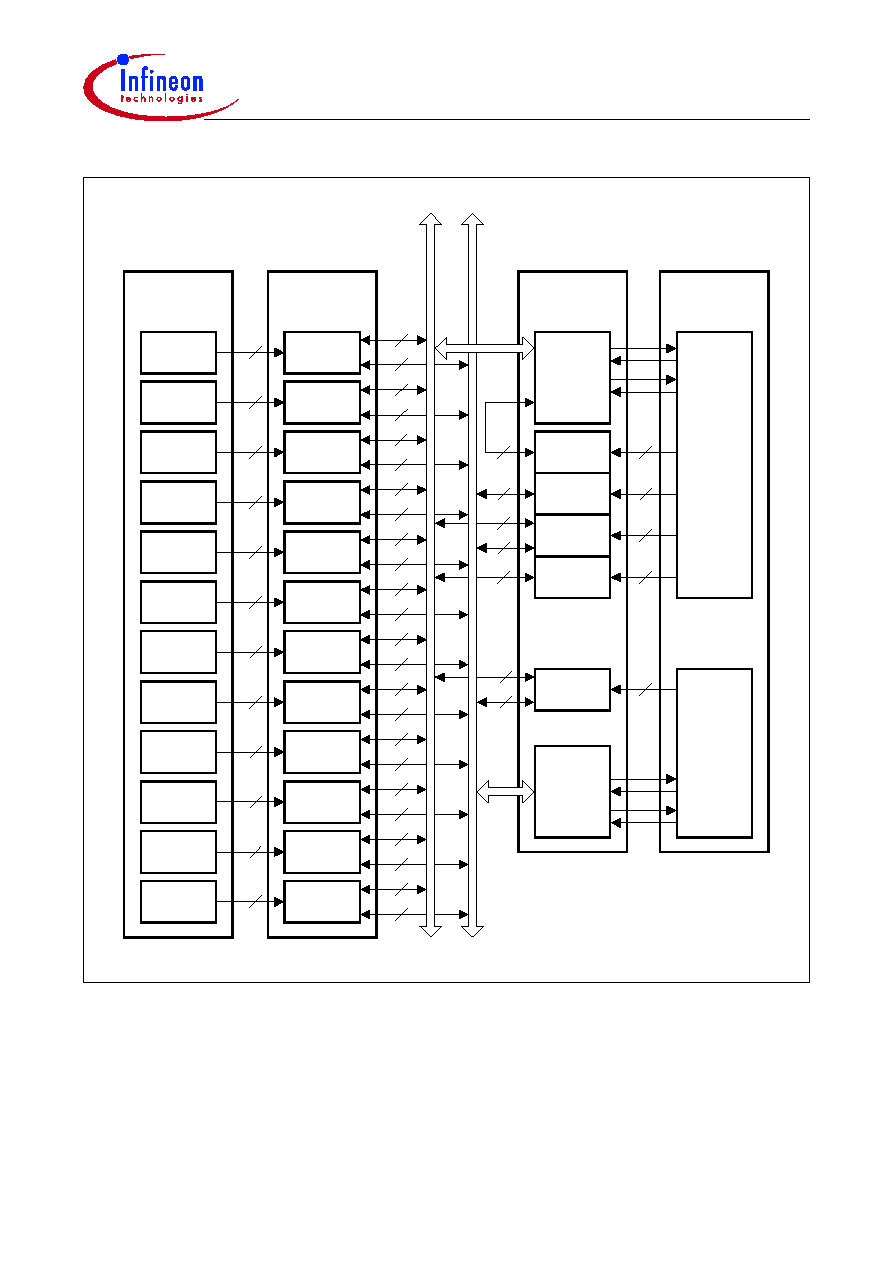
TC11IB
Data Sheet
58
V2.3, 2003-11
Figure 15
Block Diagram of the TC11IB Interrupt System
M C B 0 4 9 4 4
8 S R N s
8 S R N s
8
G P T U 0
G P T U 1
3 S R N s
3
S S C
4 S R N s
4
A S C
1 S R N
1
1 6 x 5 0
3 3 S R N s
3 3
P C I
9 S R N s
9
E th e rn e t
1 S R N
1
M M C I
2 4 S R N s
2 4
E x te rn a l
1 S R N
1
B C U 0
1 S R N
1
B C U 1
1 S R N
1
O C D S
S e rv ic e
R e q u e s t
N o d e s
S e rv ic e
R e q u e s to rs
8
8
2
3
4
4
1
1
3 3
3 3
9
9
1
1
2 4
2 4
1
1
1
1
1
1
P C P
In te rru p t
A rb itra tio n B u s
C P U
In te rru p t
A rb itra tio n B u s
2 S R N s
2 S R N s
In te rru p t
C o n tro l U n its
2
P IP N
PC P
In t. A c k .
C C P N
2
In te rru p t
S e rv ic e
P ro v id e rs
2
4
4
4 S R N s
4
P IP N
C PU
C C P N
In t. A c k .
S o ftw a re
In te rru p t
IC U
PIC U
3
8
8
8
5 S R N s
3 S R N s
5
3
5
5
3
In t. R e q .
In t. R e q .

TC11IB
Data Sheet
59
V2.3, 2003-11
Boot Options
The TC11IB booting schemes provides a number of different boot options for the start of
code execution.
Table 5
shows the boot options available in the TC11IB.
1) SSC/ASC BootStrap Loader is built in BOOT ROM which provides a mechanism to load the startup program,
which is executed after reset, via the SSC/ASC interface. After successfully loaded, the startup program will
be executed from the address at 0xC000 0004
H
.
Table 5
Boot Selections
OCDSE BRKIN
CFG
[3]
CFG
[2:0]
Type of Boot
Boot Source Initial
PC Value
1
1
X
000
B
Start directly in core
scratchpad memory
SRAM (Only
via SW
Reset)
D400 0000
H
Not
(000
or
100)
Start from Boot ROM
Boot ROM,
SSC BSL
mode
1)
(BootStrap
Loader) or
ASC BSL
mode
1)
DFFF FFFC
H
0
100
B
External memory as
slave directly via EBU
External
Memory
(non-cached,
CS0)
A000 0000
H
1
100
B
External memory as
master directly via
EBU
1
0
don't care
Tri-state chip
(deep sleep)
�
�
0
1
0
100
B
Go to halt with EBU
enabled as slave
�
�
1
Go to halt with EBU
enabled as master
all other
combina-
tions
Go to halt with EBU
disabled
0
0
don't care
Go to external
emulator space
�
DE00 0000
H

TC11IB
Data Sheet
60
V2.3, 2003-11
Power Management System
The TC11IB power management system allows software to configure the various
processing units so that they automatically adjust to draw the minimum necessary power
for the application.
There are four power management modes:
� Run Mode
� Idle Mode
� Sleep Mode
� Deep Sleep Mode
Table 6
describes these features of the power management modes.
Besides these explicit software-controlled power-saving modes, TC11IB supports
automatic power-saving in that operating units, which are currently not required or idle,
are shut off automatically until their operation is required again.
Table 6
Power Management Mode Summary
Mode
Description
Run
The system is fully operational. All clocks and peripherals are enabled,
as determined by software.
Idle
The CPU clock is disabled, waiting for a condition to return it to Run
Mode. Idle Mode can be entered by software when the processor has no
active tasks to perform. All peripherals remain powered and clocked.
Processor memory is accessible to peripherals. A reset, Watchdog Timer
event, a falling edge on the NMI pin, or any enabled interrupt event will
return the system to Run Mode.
Sleep
The system clock continues to be distributed only to those peripherals
programmed to operate in Sleep Mode. Interrupts from operating
peripherals, the Watchdog Timer, a falling edge on the NMI pin, or a reset
event will return the system to Run Mode. Entering this state requires an
orderly shut-down controlled by the Power Management State Machine.
Deep Sleep
The system clock is shut off; only an external signal will restart the
system. Entering this state requires an orderly shut-down controlled by
the Power Management State Machine (PMSM).
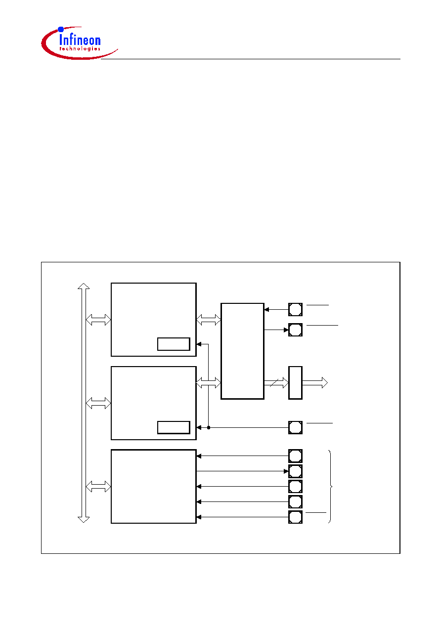
TC11IB
Data Sheet
61
V2.3, 2003-11
On-Chip Debug Support
The On-Chip Debug Support of the TC11IB consists of four building blocks:
� OCDS module in the TriCore CPU
� On-chip breakpoint hardware
� Support of an external break signal
� OCDS module in the PCP
� Special DEBUG instruction for program execution tracing
� Trace module of the TriCore
� Outputs 16 bits per cycle with pipeline status information, PC bus information, and
breakpoint qualification information
� Debugger Interface (Cerberus)
� Provided for debug purposes of emulation tool vendors
� Accessible through a JTAG standard interface with dedicated JTAG port pins
Figure 16
shows a basic block diagram of the building blocks.
.
Figure 16
OCDS Support Basic Block Diagram
M C B 0 4 9 4 7
C erberus &
JTA G
T R S T
T C K
T M S
T D I
T D O
J T A G
I/O L in e s
TriC ore
C PU
O C D S
PC P
O C D S
SC U
T ra c e
C o n tro l
1 6
B R K IN
B R K O U T
O
CDS
2
O C D S 2 [1 5 :0 ]
O C D S E
F P I B u s
TC11IB
Data Sheet
62
V2.3, 2003-11
Clock Generation Unit
The Clock Generation Unit in the TC11IB, shown in
Figure 17
, consists of an oscillator
circuit and one Phase-Locked Loop (PLL). The PLL can convert a low-frequency
external clock signal to a high-speed internal clock for maximum performance. The PLL
also has fail-safe logic that detects degenerate external clock behavior such as abnormal
frequency deviations or a total loss of the external clock. It can execute emergency
actions if it losses the lock on the external clock. PLL can provide the 96MHz and 48MHz
clocks.
In general, the Clock Generation Unit (CGU) is controlled through the System Control
Unit (SCU) module of the TC11IB.
Figure 17
Clock Generation Unit Block Diagram
1
>
M C A 0 4 9 4 0
O s c illa to r
C irc u it
X T A L 1
X T A L 2
f
O S C
P h a s e
D e te c t.
V C O
N
D iv id e r
P L L
f
V C O
1
0
K :1
D iv id e r
f
S Y S
=
9 6 M H z
S y s te m _
C L K
L o c k
D e te c to r
O S C _ F A IL
P L L
L o c k e d
D e e p
S le e p
N D IV
[5 :0 ]
V C O _
B Y P A S S
K D IV
[3 :0 ]
P L L _
B Y P A S S
System C ontrol U nit
SC U
R e g is te r P L L _ C L C
M U X
1
0
M U X
K :2
D iv id e r
V C O _
S E L
[1 :0 ]
f
S Y S
=
4 8 M H z
S y s te m _
C L K
1
0
M U X
P L L _
2 E N
P L L _
2 S E L
C lock G eneration U nit
C G U
TC11IB
Data Sheet
63
V2.3, 2003-11
Recommended Oscillator Circuits
Figure 18
Oscillator Circuitries
For the main oscillator of the TC11IB the following external passive components are
recommended:
� Crystal: 12 MHz
� C1, C2: 10 pF
A block capacitor between
V
DDOSC
and
V
SSOSC
is recommended, too.
T C 1 1 IB
O s c illa to r
M C S 0 4 9 4 8
T C 1 1 IB
O s c illa to r
V
D D O S C
V
S S O S C
C
1
1 2
M H z
C
2
X T A L 1
X T A L 2
V
D D O S C
V
S S O S C
X T A L 1
X T A L 2
E x te rn a l
C lo c k S ig n a l
TC11IB
Data Sheet
64
V2.3, 2003-11
Power Supply
The TC11IB provides an ingenious power supply concept in order to improve the EMI
behavior as well as to minimize the crosstalk within on-chip modules.
Figure 19
shows the TC11IB's power supply concept, where certain logic modules are
individually supplied with power. This concept improves the EMI behavior by reduction
of the noise cross coupling.
Figure 19
TC11IB Power Supply Concept
M C B 0 4 9 5 3
P C P
M e m o ry
D M U
P M U
C o m D R A M
P C I
P o rts
C P U &
P e rip h e ra l
L o g ic
G P IO
P o rts
(P 0 -P 5 )
E B U
P o rts
P L L
O S C
L M U
V
D D D R A M
V
S S
V
C O M R E F
V
S S
V
D D P
(3 .3 V )
V
S S
V
D D P L L 9 6
V
S S P L L 9 6
V
D D O S C
V
S S O S C
V
S S
V
L M U R E F
V
S S
V
D D D R A M
V
S S
(1 .8 V )
V
D D

TC11IB
Data Sheet
65
V2.3, 2003-11
Power Sequencing
During power-up, the reset pin PORST has to be held active until both power supply
voltages have reached at least their minimum values.
While powering up (rising of the supply voltages from 0V to their regular operating
values), it has to be ensured, that the core power supply V
DD
reaches its operating value
first, and then the GPIO power supply V
DDP
. During the rising time of the core power
supply it must be ensured that 0 < V
DD
- V
DDP
< 0.5V.
During power-down, the core and GPIO power supplies V
DD
and V
DDP
respectively,
have to be switched off completely until all capacitances are discharged to zero, before
the next power-up.
Note: The state of the pins are undefined when only the port voltage V
DDP
is switched
on.

TC11IB
Data Sheet
66
V2.3, 2003-11
Identification Register Values
Table 7
TC11IB Identification Registers
Short Name
Address
Value
SCU_ID
F000 0008
H
0013 C002
H
MANID
F000 0070
H
0000 1820
H
CHIPID
F000 0074
H
0000 8502
H
RTID
F000 0078
H
0000 0000
H
BCU1_ID
F000 0208
H
0000 6A06
H
STM_ID
F000 0308
H
0000 C002
H
JPD_ID
F000 0408
H
0000 6302
H
GPTU0_ID
F000 0608
H
0001 C002
H
GPTU1_ID
F000 0708
H
0001 C002
H
ASC_ID
F000 0808
H
0000 4461
H
16X50_ID
F000 0908
H
0012 C001
H
SSC_ID
F000 0A08
H
0000 4503
H
MMCI_ID
F000 0B08
H
0000 5B01
H
PCP_ID
F000 3F08
H
0020 C002
H
PCI_ID
F040 0034
H
0001 15D1
H
PCI_SUBID
F040 0038
H
0000 15D1
H
PCI_CS1_ID
F100 0000
H
0001 15D1
H
PCI_CS1_SUBID
F100 002C
H
0001 15D1
H
PCI_CS2_ID
F100 0100
H
0001 15D1
H
PCI_CS2_SUBID
F100 012C
H
0002 15D1
H
BCU0_ID
F200 0008
H
0000 6A06
H
CPU_ID
F7E0 FF18
H
0015 C004
H
MMU_ID
F7E1 8008
H
0009 C002
H
EBU_ID
F800 0008
H
0014 C003
H
LMU_ID
F800 0410
H
0016 C001
H
DMU_ID
F87F FC08
H
0008 C002
H
PMU_ID
F87F FD08
H
000B C002
H
LCU_ID
F87F FE08
H
000F C003
H
LFI_ID
F87F FF08
H
000C C003
H

TC11IB
Data Sheet
67
V2.3, 2003-11
Absolute Maximum Ratings
Note: Stresses above those listed under "Absolute Maximum Ratings" may cause
permanent damage to the device. This is a stress rating only and functional
operation of the device at these or any other conditions above those indicated in
the operational sections of this specification is not implied. Exposure to absolute
maximum rating conditions for extended periods may affect device reliability.
During absolute maximum rating overload conditions (
V
IN
>
V
DD
or
V
IN
<
V
SS
) the
voltage on
V
DD
pins with respect to ground (
V
SS
) must not exceed the values
defined by the absolute maximum ratings.
Parameter
Symbol
Limit Values
Unit Notes
min.
max.
Ambient temperature
T
A
-
25
85
�C
under bias
Storage temperature
T
ST
-
65
150
�C
Junction temperature
T
J
�
110
�C
under bias
Voltage on I/O Supply pins
with
respect to ground (
V
SS
)
V
DDP
�0.5
4.5
V
Voltage on Core Supply pins
with respect to ground (
V
SS
)
V
DD
�0.3
2.4
V
Voltage on PLL Supply pins
with respect to ground (
V
SS
)
V
DDPLL
�0.3
2.4
V
Voltage on Oscillator Supply
pins with respect to ground
(
V
SS
)
V
DDOSC
�0.3
2.4
V
Voltage on eDRAM Supply pins
with respect to ground (
V
SS
)
V
DDDRAM
�0.3
2.4
V
Voltage on any pin with respect
to ground (
V
SS
)
V
IN
-
0.5
4.5
V
Input current on any pin during
overload condition
I
IN
-10
10
mA
Absolute sum of all input
currents during overload
condition
I
IN
�
|100|
mA
Power dissipation
P
DISS
�
1.6
W
TC11IB
Data Sheet
68
V2.3, 2003-11
Operating Conditions
The following operating conditions must not be exceeded in order to ensure correct
operation of the TC11IB. All parameters specified in the following sections refer to these
operating conditions, unless otherwise noticed.
Parameter Interpretation
The parameters listed in the following partly represent the characteristics of the TC11IB
and partly its demands on the system. To aid in interpreting the parameters right, when
evaluating them for a design, they are marked in column "Symbol":
CC (Controller Characteristics):
The logic of the TC11IB will provide signals with the respective characteristics.
SR (System Requirement):
The external system must provide signals with the respective characteristics to the
TC11IB.
Parameter
Symbol
Limit Values
Unit Notes
min.
max.
Supply voltage
V
DDP
3.0
3.6
V
I/O supply
V
DD
1.71
1.89
V
Core supply
V
DDPLL
1.71
1.89
V
PLL supply
V
DDOSC
1.71
1.89
V
Oscillator supply
V
DDDRAM
1.71
1.89
V
eDRAM supply
Ground voltage
V
SS
0
V
Ambient temperature
under bias
T
A
-
25
85
�C
CPU clock
f
CPU
�
96
MHz
External Load
Capacitance
C
L
�
50
pF
TC11IB
Data Sheet
69
V2.3, 2003-11
DC Characteristics
DC-Characteristics
V
SS
= 0 V; T
A
= -25
�
C to +85
�
C
Parameter
Symbol
Limit Values
Unit Test Condition
min.
max.
GPIO pins, Dedicated pins and EBU pins
Input low voltage
V
IL
SR
�
0.8
V
Input high voltage
V
IH
SR
2.0
�
V
Output low voltage
V
OL
CC
�
0.4
V
Output high voltage
V
OH
CC
2.4
�
V
Pull-up current
1)
I
PUB
CC
-
37
-
12
�
A
V
IN
= 0V
I
PUC
CC
-
12
-
2
�
A
V
IN
= 0V
Pull-down current
2)
I
PDA
CC
55
220
�
A
V
IN
= V
DDP
I
PDC
CC
2
14
�
A
V
IN
= V
DDP
Input leakage current
3)
I
OZ2
CC
�
�
1
�
A
0 <
V
IN
<
V
DDP
Pin Capacitance
4)
C
IO
CC
�
10
pF
PCI pins
Input low voltage
V
ILP
SR
-
0.5
0.3
V
DDP
V
Input high voltage
V
IHP
SR
0.5
V
DDP
V
DDP
+
0.5
V
Output low voltage
V
OLP
CC
�
0.1
V
DDP
V
I
OLP
= 1500
�
A
Output high voltage
V
OHP
CC
0.9
V
DDP
�
V
I
OHP
=
-
500
�
A
Input Pull-up voltage
5)
V
IPU
CC
0.7
V
DDP
�
Input leakage current
6)
I
IL
CC
�
�
10
�
A
0 <
V
IN
<
V
DDP
PME input leakage
7)
I
OFF
CC
�
1
�
A
V
IN
3.6V
V
DD
off or
floating
Input pin capacitance
8)
C
IN
CC
�
10
pF
CLK pin capacitance
C
CLK
CC
5
12
pF
TC11IB
Data Sheet
70
V2.3, 2003-11
IDSEL pin capacitance
9)
C
IDSEL
CC �
8
pF
Pin inductance
L
PIN
CC
�
20
nH
Oscillator Pins
Input low voltage at XTAL1
V
ILX
SR
-0.3
0.3
�
V
DDOSC
V
Input high voltage at XTAL1
V
IHX
SR
0.7
�
V
DDOSC
2.4
V
Notes:
1)
The current is applicable to the pins, for which a pull up has been specified. Refer to
Table 1
. I
PUx
refers to the
pull up current for type x.
2)
The current is applicable to the pins, for which a pull down has been specified. Refer to
Table 1
. I
PDx
refers to
the pull down current for type x.
3)
Pins with internal pull up or pull down are not included.
4)
Not 100% tested, guaranteed by design characterization.
5)
This specification is guaranteed by design. It is the minimum voltage to which pull up resistors are calculated
to pull a floated network. Applications sensitive to static power utilization must assure that the input buffer is
conducting minimum current at this input voltage.
6)
Input leakage currents include high impedance output leakage for all bi-directional buffers with tristate outputs.
7)
This input leakage is the maximum allowable leakage into the PME open drain driver when power is removed
from VDD of the component. This assumes that no event has occurred to cause the device to attempt to assert
PME.
8)
Absolute maximum pin capacitance for a PCI input is 10pF (except for CLK). Exceptions are granted to
motherboard-only devices up to 16pF.
9)
Lower capacitance on this input-only pin allows for non-resistive coupling to AD[xx].
DC-Characteristics(cont'd)
V
SS
= 0 V; T
A
= -25
�
C to +85
�
C
Parameter
Symbol
Limit Values
Unit Test Condition
min.
max.
TC11IB
Data Sheet
71
V2.3, 2003-11
Power Supply Current
Parameter
Symbol
Limit values
Unit
Test Conditions
typ.
1)
1)
Typical values are measured at 25�C, CPU clock at 96MHz and nominal supply voltage, i.e. 3.3V for V
DDP
and
1.8V for V
DD
, V
DDPLL
, V
DDOSC
and V
DDDRAM
. These currents are measured using a typical application pattern.
The power consumption of modules can increase or decrease using other application programs. The PLL is
bypassed while PCI and MMCI modules are inactive.
max.
Active mode supply
current
I
DD
481.9
629
mA
Sum of
I
DDS
2)
2)
These power supply currents are defined as the sum of all currents at the V
DD
power supply lines:
V
DD
+ V
DDP
+ V
DDDRAM
+ V
DDPLL
+ V
DDOSC
412.9
519
mA
I
DD
at
V
DD
3)
3)
This measurement includes the TriCore and Logic power supply lines.
44.0
60
mA
I
DD
at
V
DDP
25.0
50
mA
I
DD
at
V
DDDRAM
Idle mode supply current
I
ID
213.0
308
mA
Sum of
I
DDS
2)4)
4)
CPU is in idle state, input clock to all peripherals are enabled,
195.8
259
mA
I
DD
at
V
DD
3)4)
6.5
20
mA
I
DD
at
V
DDP
4)
10.7
29
mA
I
DD
at
V
DDDRAM
4)
Sleep mode supply
current
I
SL
195.4
288
mA
Sum of
I
DDS
2)5)6)
5)
Input clock to all peripherals are disabled.
6)
The values are not subject to production test - verified by characterization only.
178.2
239
mA
I
DD
at
V
DD
3)5)6)
6.5
20
mA
I
DD
at
V
DDP
5)6)
10.7
29
mA
I
DD
at
V
DDDRAM
5)6)
Deep sleep mode supply
current
I
DS
11.2
69
mA
Sum of
I
DDS
2)7)
7)
Clock generation is disabled at the source.
6.7
41
mA
I
DD
at
V
DD
3)7)
0.3
10
mA
I
DD
at
V
DDP
7)
4.2
18
mA
I
DD
at
V
DDDRAM
7)
TC11IB
Data Sheet
72
V2.3, 2003-11
AC Characteristics
(Operating Conditions apply)
Figure 20
Input/Output Waveforms for AC Tests
- for GPIO, Dedicated and EBU pins
2.0V
0.8V
test points
2.0V
0.8V
2.4V
0.4V
AC inputs during testing are driven at 2.4V for a logic "1" and 0.4V for a logic "0".
Timing measurements are made at V
IHmin
for a logic "1" and V
ILmax
for a logic "0".

TC11IB
Data Sheet
73
V2.3, 2003-11
Input Clock Timing
(Operating Conditions apply)
Figure 21
Input Clock Timing
Parameter
Symbol
Limits
Unit
min
max
Oscillator clock frequency
with PLL
f
OSC
SR
12
MHz
Input clock frequency driving at
XTAL1
with PLL
f
OSCDD
SR
12
MHz
Input Clock high time
t
1
SR 37.5
-
ns
Input Clock low time
t
2
SR 37.5
-
ns
Input Clock rise time
t
3
SR
-
4.1
ns
Input Clock fall time
t
4
SR
-
4.1
ns
Input Clock
at XTAL1
t
4
V
IHX
t
3
t
1
V
ILX
t
2
t
OSCDD
0.5 V
DD
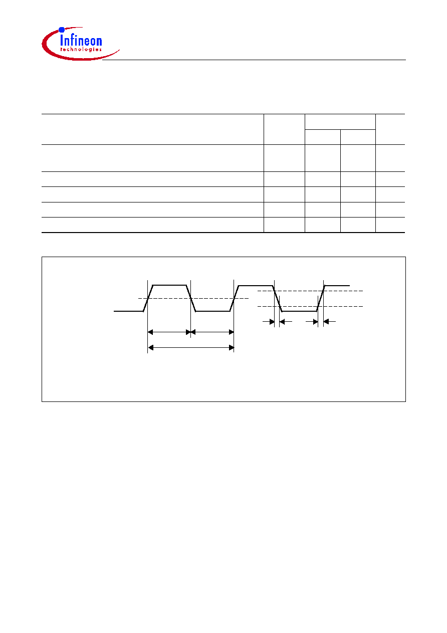
TC11IB
Data Sheet
74
V2.3, 2003-11
CPU Clock Timing
(Operating Conditions apply; C
L
= 50 pF)
Figure 22
CPUCLK Timing
Parameter
Symbol
Limits
Unit
min
max
CPUCLK period
t
CPUCLK
CC
10.4
-
ns
CPUCLK high time
t
1
CC
3
-
ns
CPUCLK low time
t
2
CC
4.5
-
ns
CPUCLK rise time
t
3
CC
-
2.8
ns
CPUCLK fall time
t
4
CC
-
2.2
ns
CPUCLK
t
4
0.9 V
DD
t
3
t
1
0.1 V
DD
t
2
t
CPUCLK
0.5 V
DD

TC11IB
Data Sheet
75
V2.3, 2003-11
Timing for eDRAM Refresh Cycle
(Operating Conditions apply; C
L
= 50 pF)
Figure 23
eDRAM Refresh Cycle Timing
Parameter
Symbol
Limits
Unit
min
max
eDRAM retention time
t
TRET
CC
-
16
ms
LMU eDRAM refresh cycle time
t
REF
CC
-
1.6
�
s
ComDRAM eDRAM refresh cycle time
t
REF
CC
-
0.8
�
s
Refresh Cycle Time t
REF
Refresh
Refresh
eDRAM access
Access Cycle Time
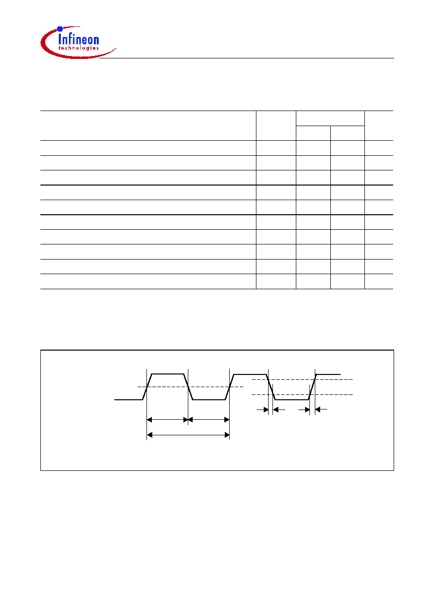
TC11IB
Data Sheet
76
V2.3, 2003-11
Timing for EBU_LMB Clock Outputs
(Operating Conditions apply; C
L
= 50 pF)
Figure 24
EBU_LMB Clock Output Timing
Parameter
Symbol
Limits
Unit
min
max
EBUCLK period
1)
1)
LMB Clock : EBUCLK Clock = 1:1 (EBU_EBUCON.BUSCLK = 00
H
).
t
1
CC
10.4
-
ns
EBUCLK high time
t
2
CC
4.5
-
ns
EBUCLK low time
t
3
CC
3
-
ns
EBUCLK rise time
t
4
CC
-
2.5
ns
EBUCLK fall time
t
5
CC
-
2.5
ns
ACLK period
2)
2)
LMB Clock : ACLK Clock = 2:1 (EBU_BFCON.EXTCLK = 01
H
). If EBU_BFCON.EXTCLK = 10
H
, the duty cycle
is 33%, not 50%.
t
6
CC
20
-
ns
ACLK high time
t
7
CC
9
-
ns
ACLK low time
t
8
CC
9
-
ns
ACLK rise time
t
9
CC
-
3.5
ns
ACLK fall time
t
10
CC
-
2.5
ns
EBUCLK /
ACLK
0.9 V
DD
0.1 V
DD
t
1
(t
6
)
0.5 V
DD
t
2
(t
7
)
t
3
(t
8
)
t
5
(t
10
)
t
4
(t
9
)

TC11IB
Data Sheet
77
V2.3, 2003-11
Timing for SDRAM Access Signals
(Operating Conditions apply; C
L
= 30 pF)
Parameter
Symbol
Limits
Unit
min
max
CKE high from EBUCLK
t
1
CC
-
7.0
ns
CKE low from EBUCLK
t
2
CC
-
7.0
ns
A(23:0) output valid from EBUCLK
t
3
CC
-
8.0
ns
A(23:0) output hold from EBUCLK
t
4
CC 2.0
-
ns
CS(6:0) low from EBUCLK
t
5
CC
-
7.0
ns
CS(6:0) high from EBUCLK
t
6
CC
-
7.0
ns
RAS low from EBUCLK
t
7
CC
-
7.0
ns
RAS high from EBUCLK
t
8
CC
-
8.0
ns
CAS low from EBUCLK
t
9
CC
-
7.0
ns
CAS high from EBUCLK
t
10
CC
-
8.0
ns
RD/WR low from EBUCLK
t
11
CC
-
7.5
ns
RD/WR high from EBUCLK
t
12
CC
-
7.5
ns
BC(3:0) low from EBUCLK
t
13
CC
-
7.0
ns
BC(3:0) high from EBUCLK
t
14
CC
-
7.0
ns
AD(31:0) output valid from EBUCLK
t
15
CC
-
7.7
ns
AD(31:0) output hold from EBUCLK
t
16
CC 2.0
-
ns
AD(31:0) input setup to EBUCLK
t
17
SR 0.6
-
ns
AD(31:0) input hold from EBUCLK
t
18
SR 3.8
-
ns
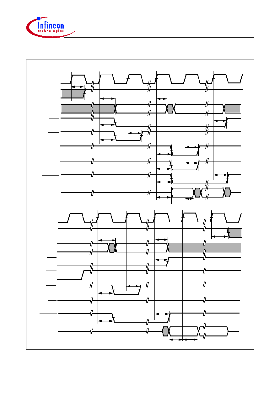
TC11IB
Data Sheet
78
V2.3, 2003-11
Figure 25
SDRAM Access Timing
t
6
t
9
t
13
t
14
column
EBUCLK
A(23:0)
CSx
AD(31:0)
t
1
t
4
EBUCLK
CKE
t
3
RAS
CAS
RD/WR
t
5
t
6
t
15
t
16
row
data
t
7
t
8
t
9
t
10
t
11
t
12
BC(3:0)
t
13
t
14
data
column
EBUCLK
A(23:0)
CSx
AD(31:0)
EBUCLK
CKE
RAS
CAS
RD/WR
t
17
t
18
data
BC(3:0)
data
Read Access:
Write Access:
row
t
10
t
2
t
4
t
3
(n-1)
(0)
(0)
(n-1)
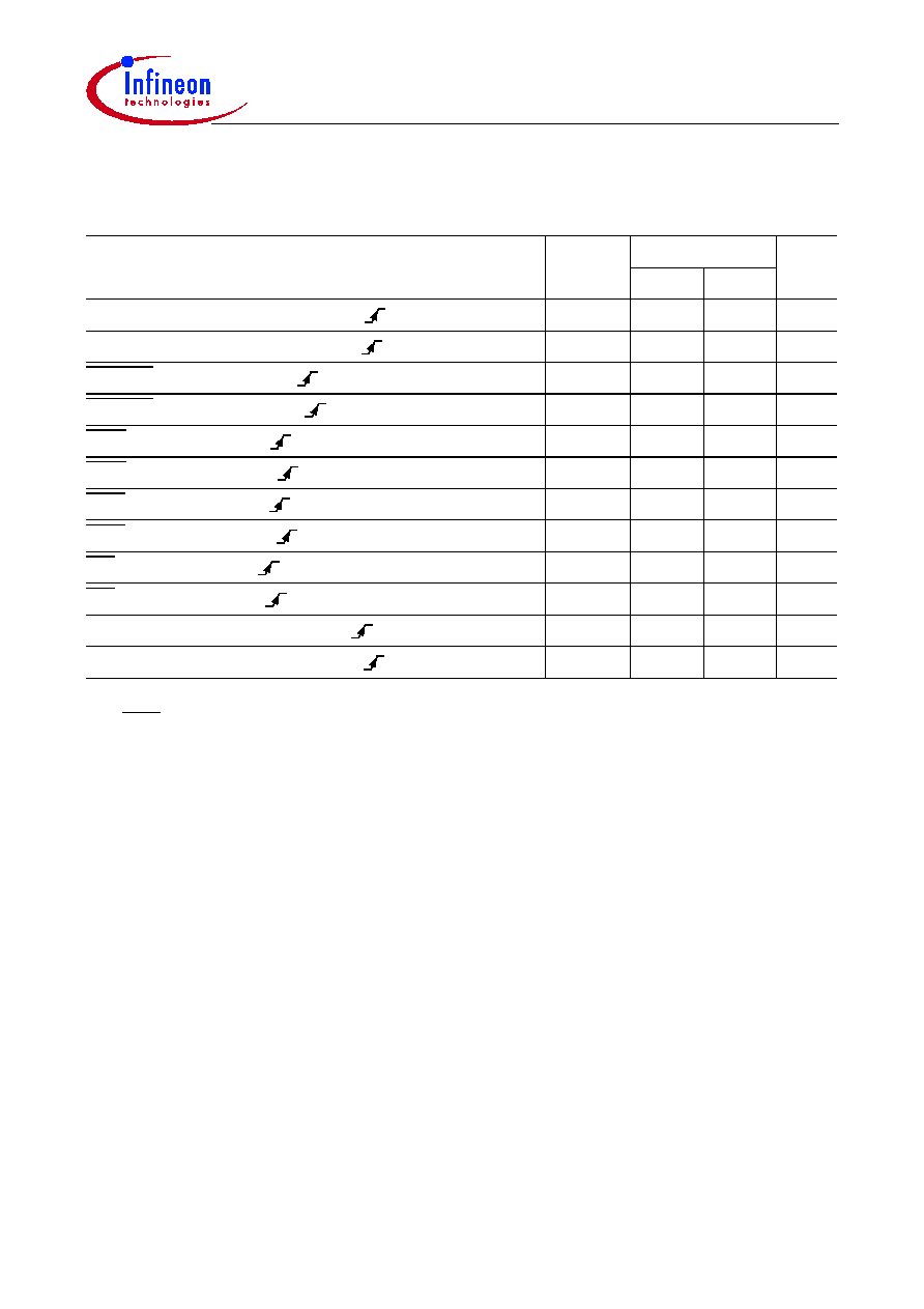
TC11IB
Data Sheet
79
V2.3, 2003-11
Timing for Burst Flash Access Signals
Operating Conditions apply; C
L
= 50 pF)
Note:WAIT signal is not characterized here because the TC11IB does not cover such cases.
Parameter
Symbol
Limits
Unit
min
max
A(23:0) output valid from ACLK
t
1
CC
-
11.0
ns
A(23:0) output hold from ACLK
t
2
CC 2.0
-
ns
CS(6:0) low from ACLK
t
3
CC
-
9.0
ns
CS(6:0) high from ACLK
t
4
CC
-
9.0
ns
ADV low from ACLK
t
5
CC
-
10.0
ns
ADV high from ACLK
t
6
CC
-
10.0
ns
BAA low from ACLK
t
7
CC
-
10.0
ns
BAA high from ACLK
t
8
CC
-
10.0
ns
RD low from ACLK
t
9
CC
-
12.0
ns
RD high from ACLK
t
10
CC
-
10.0
ns
AD(31:0) input setup to ACLK
t
11
SR 8.0
-
ns
AD(31:0) input hold from ACLK
t
12
SR 1.0
-
ns

TC11IB
Data Sheet
80
V2.3, 2003-11
Figure 26
Burst Flash Access Timing
A(23:0)
CS
x
AD(3
1:
0)
ADV
BAA
RD
t
3
t
4
a
ddres
s
t
5
t
6
t
7
t
8
t
10
data(0)
ACLK
t
1
t
9
data(n-1
)
t
11
t
12
t
2

TC11IB
Data Sheet
81
V2.3, 2003-11
Timing for Demultiplexed Access Signals
(Operating Conditions apply; C
L
= 50 pF)
Parameter
Symbol
Limits
Unit
min
max
ALE low from EBUCLK
t
1
CC
-
8.0
ns
ALE high from EBUCLK
t
2
CC
-
8.0
ns
A(23:0) output valid from EBUCLK
t
3
CC
-
8.0
ns
A(23:0) output hold from EBUCLK
t
4
CC 2.0
-
ns
CS(6:0) low from EBUCLK
t
5
CC
-
8.0
ns
CS(6:0) high from EBUCLK
t
6
CC
-
8.0
ns
MR/W low from EBUCLK
t
7
CC
-
8.0
ns
MR/W high from EBUCLK
t
8
CC
-
8.0
ns
RMW low from EBUCLK
t
9
CC
-
16.5
ns
RMW high from EBUCLK
t
10
CC
-
16.5
ns
RD low from EBUCLK
t
11
CC
-
8.0
ns
RD high from EBUCLK
t
12
CC
-
8.0
ns
RD/WR low from EBUCLK
t
13
CC
-
8.0
ns
RD/WR high from EBUCLK
t
14
CC
-
8.0
ns
CMDELAY input setup to EBUCLK
t
15
SR 7.0
-
ns
CMDELAY hold from EBUCLK
t
16
SR 5.5
-
ns
WAIT input setup to EBUCLK
t
17
SR 8.0
-
ns
WAIT hold from EBUCLK
t
18
SR 5.5
-
ns
BC(3:0) low from EBUCLK
t
19
CC
-
8.0
ns
BC(3:0) high from EBUCLK
t
20
CC
-
8.0
ns
AD(31:0) output valid from EBUCLK
t
21
CC
-
8.0
ns
AD(31:0) output hold from EBUCLK
t
22
CC 2.0
-
ns
AD(31:0) input setup to EBUCLK
t
23
SR 7.0
-
ns
AD(31:0) input hold from EBUCLK
t
24
SR 3.5
-
ns
TC11IB
Data Sheet
82
V2.3, 2003-11
Figure 27
Write Access in Demultiplexed Access
EBUCLK
A(23
:0)
CS
x
AD(
31:0
)
t
1
t
2
EBUCLK
ALE
t
3
MR/W
RD
/WR
CM
DELAY
t
5
t
6
t
21
t
22
a
ddr
ess
da
ta
t
7
t
15
t
16
t
13
t
4
WAIT
t
14
BC(
3
.0)
t
19
t
20
t
20
t
19
t
17
t
18
TC11IB
Data Sheet
83
V2.3, 2003-11
Figure 28
Read Access in Demultiplexed Access
EB
UCL
K
A(2
3
:0)
CSx
AD(31:
0)
t
1
t
2
EB
UCL
K
ALE
t
3
MR
/W
RD
CMDEL
A
Y
t
5
t
6
t
23
t
24
ad
dres
s
data
t
11
t
4
WAIT
RM
W
t
9
t
12
t
17
t
18
BC(3:0
)
t
19
t
8
t
20
t
19
t
15
t
16
t
10
Note: RMW
s
i
g
nal is
on
ly
av
aila
ble d
u
ring
Re
ad-Mo
dify
-Write
Ac
ces
s
.

TC11IB
Data Sheet
84
V2.3, 2003-11
Timing for Multiplexed Access Signals
(Operating Conditions apply; C
L
= 50 pF)
Parameter
Symbol
Limits
Unit
min
max
ALE high from EBUCLK
t
1
CC
-
8.0
ns
ALE low from EBUCLK
t
2
CC
-
8.0
ns
AD(31:0) output valid from EBUCLK
t
3
CC
-
8.0
ns
AD(31:0) output hold from EBUCLK
t
4
CC 2.0
-
ns
AD(31:0) input setup to EBUCLK
t
5
SR 7.0
-
ns
AD(31:0) input hold from EBUCLK
t
6
SR 3.5
-
ns
CS(6:0) low from EBUCLK
t
7
CC
-
8.0
ns
CS(6:0) high from EBUCLK
t
8
CC
-
8.0
ns
MR/W low from EBUCLK
t
9
CC
-
8.0
ns
MR/W high from EBUCLK
t
10
CC
-
8.0
ns
RMW low from EBUCLK
t
11
CC
-
16.5
ns
RMW high from EBUCLK
t
12
CC
-
16.5
ns
RD/WR low from EBUCLK
t
13
CC
-
8.0
ns
RD/WR high from EBUCLK
t
14
CC
-
8.0
ns
RD low from EBUCLK
t
15
CC
-
8.0
ns
RD high from EBUCLK
t
16
CC
-
8.0
ns
CMDELAY input setup to EBUCLK
t
17
SR 7.0
-
ns
CMDELAY hold from EBUCLK
t
18
SR 5.5
-
ns
WAIT input setup to EBUCLK
t
19
SR 6.0
-
ns
WAIT hold from EBUCLK
t
20
SR 5.5
-
ns
BC(3:0) low from EBUCLK
t
21
CC
-
8.0
ns
BC(3:0) high from EBUCLK
t
22
CC
-
8.0
ns

TC11IB
Data Sheet
85
V2.3, 2003-11
Figure 29
Write Access in Multiplexed Access
EB
U
C
LK
AD(31:0
)
CSx
t
1
t
2
EB
U
C
LK
ALE
t
3
MR/W
RD
/WR
CMDE
LAY
t
7
t
8
addr
es
s
t
9
t
20
t
19
t
13
t
4
WA
IT
t
14
BC
(3.0)
t
21
t
22
t
22
t
21
dat
a
t
3
t
4
t
17
t
18
TC11IB
Data Sheet
86
V2.3, 2003-11
Figure 30
Read Access in Multiplexed Access
EB
U
C
LK
AD(31:0
)
CSx
t
1
t
2
EB
U
C
LK
ALE
t
3
MR/W
RD
CM
D
E
LAY
t
7
t
8
ad
dre
s
s
t
17
t
6
WA
IT
RM
W
t
16
t
18
BC(
3
:0)
t
21
t
10
t
22
t
21
t
15
t
4
dat
a
t
5
t
19
t
20
t
11
t
12
No
te:
RM
W
signa
l is a
v
a
i
lable on
ly du
ri
ng
Rea
d
-M
odify-Write Acce
ss.
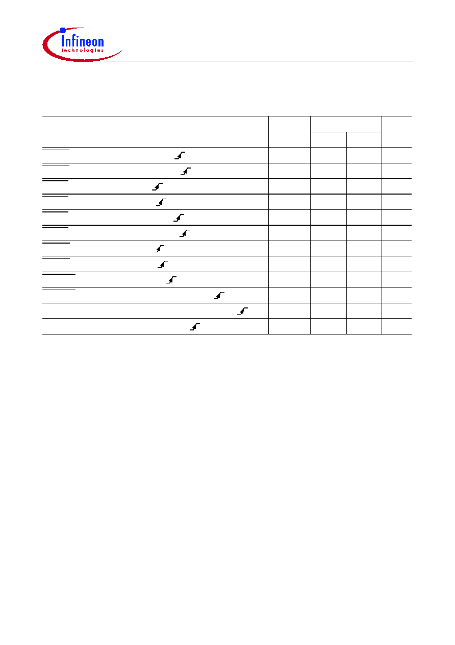
TC11IB
Data Sheet
87
V2.3, 2003-11
Timing for External Bus Arbitration Signals
(Operating Conditions apply; C
L
= 50 pF)
Parameter
Symbol
Limits
Unit
min
max
HOLD input setup to EBUCLK
t
1
SR 6.0
-
ns
HOLD input hold from EBUCLK
t
2
SR 5.5
-
ns
HLDA low from EBUCLK
t
3
CC
-
11.0
ns
HLDA high from EBUCLK
t
4
CC
-
11.0
ns
HLDA input setup to EBUCLK
t
5
SR 6.4
-
ns
HLDA input hold from EBUCLK
t
6
SR 5.5
-
ns
BREQ low from EBUCLK
t
7
CC
-
9.5
ns
BREQ high from EBUCLK
t
8
CC
-
9.5
ns
CS(6:0) drive from EBUCLK
t
9
CC
-
8.0
ns
CS(6:0) high-impedance from EBUCLK
t
10
CC
-
8.0
ns
Other signals high-impedance from EBUCLK
t
11
CC
-
8.0
ns
Other signals drive from EBUCLK
t
12
CC
-
8.0
ns
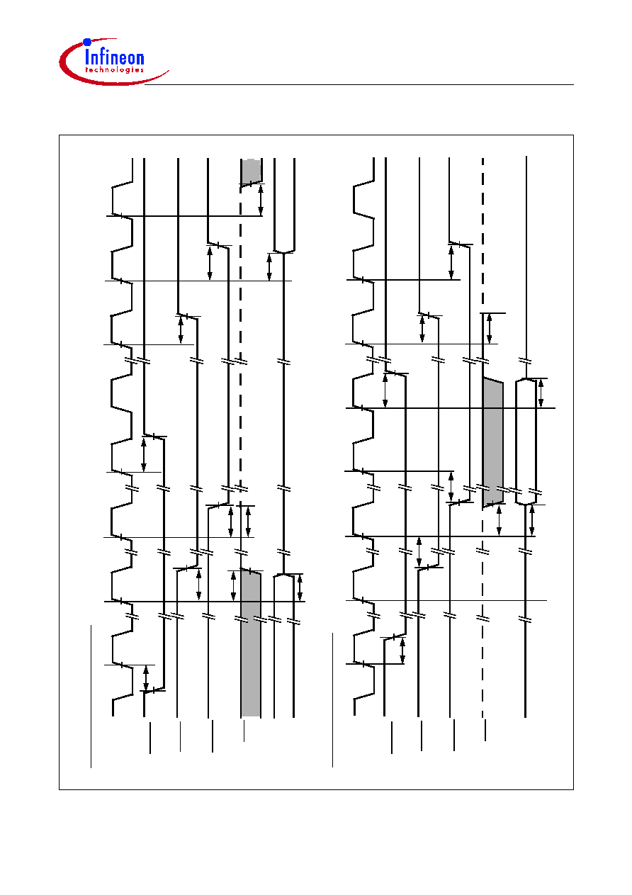
TC11IB
Data Sheet
88
V2.3, 2003-11
Figure 31
External Bus Arbitration Timing
EB
U
C
LK
HLD
A
EB
U
C
LK
BR
E
Q
CSx
t
3
HO
LD
t
1
t
7
Othe
r
s
i
gna
ls
t
9
t
11
t
2
t
4
t
8
t
9
t
12
t
10
EB
UCLK
HL
DA
EB
UCLK
HO
LD
CSx
t
5
BR
E
Q
t
7
t
1
Other
si
gnals
t
12
t
8
t
6
t
2
t
10
t
11
t
9
External Slave Mode:
External M
a
ster M
o
de:

TC11IB
Data Sheet
89
V2.3, 2003-11
Port Timing
(Operating Conditions apply; C
L
= 50 pF)
Figure 32
Port Timing
Parameter
Symbol
Limits
Unit
min
max
Port data valid from CPUCLK
1)
1)
Port data is output with respect to the slow FPI clock at 48MHz. The CPUCLK is used as a reference here
since the slow FPI clock is not available as an external pin. Port lines maintain its state for at least 2 CPU
clocks.
t
1
CC
-
14.0
ns
CPUCLK
Old State
New State
t
1
Port Lines
S_FPI_CLK

TC11IB
Data Sheet
90
V2.3, 2003-11
Timing for Ethernet Signals
(Operating Conditions apply; C
L
= 50 pF)
Note: Any other parameters which are not stated here, please refer to ANSI/IEEE Std 802.3, Section 22.3.
Parameter
Symbol
Limits
Unit
min
max
ETXCLK period (10 Mbps Ethernet)
t
1
SR 400.0
-
ns
ETXCLK high time (10 Mbps Ethernet)
t
2
SR 140.0
260.0
ns
ETXCLK low time (10 Mbps Ethernet)
t
3
SR 140.0
260.0
ns
ETXCLK period (100 Mbps Ethernet)
t
1
SR 40.0
-
ns
ETXCLK high time (100 Mbps Ethernet)
t
2
SR 14.0
26.0
ns
ETXCLK low time (100 Mbps Ethernet)
t
3
SR 14.0
26.0
ns
ERXCLK period (10 Mbps Ethernet)
t
1
SR 400.0
-
ns
ERXCLK high time (10 Mbps Ethernet)
t
2
SR 140.0
260.0
ns
ERXCLK low time (10 Mbps Ethernet)
t
3
SR 140.0
260.0
ns
ERXCLK period (100 Mbps Ethernet)
t
1
SR 40.0
-
ns
ERXCLK high time (100 Mbps Ethernet)
t
2
SR 14.0
26.0
ns
ERXCLK low time (100 Mbps Ethernet)
t
3
SR 14.0
26.0
ns
ERXD(3:0) input setup to ERXCLK
t
4
SR 10.0
-
ns
ERXD(3:0) input hold from ERXCLK
t
5
SR -
10.0
ns
ERXDV input setup to ERXCLK
t
4
SR 10.0
-
ns
ERXDV input hold from ERXCLK
t
5
SR -
10.0
ns
ERXER input setup to ERXCLK
t
4
SR 10.0
-
ns
ERXER input hold from ERXCLK
t
5
SR -
10.0
ns
ETXD(3:0) output valid from ETXCLK
t
6
CC -
25.0
ns
ETXEN output valid from ETXCLK
t
6
CC -
25.0
ns
ETXER output valid from ETXCLK
t
6
CC -
25.0
ns
EMDC clock period
t
7
CC 150.0
-
ns
EMDIO input setup to EMDC (sourced by STA)
t
8
SR 10.0
-
ns
EMDIO input hold from EMDC (sourced by STA)
t
9
SR -
10.0
ns
EMDIO output valid from EMDC (sourced by PHY)
t
10
CC -
300.0
ns
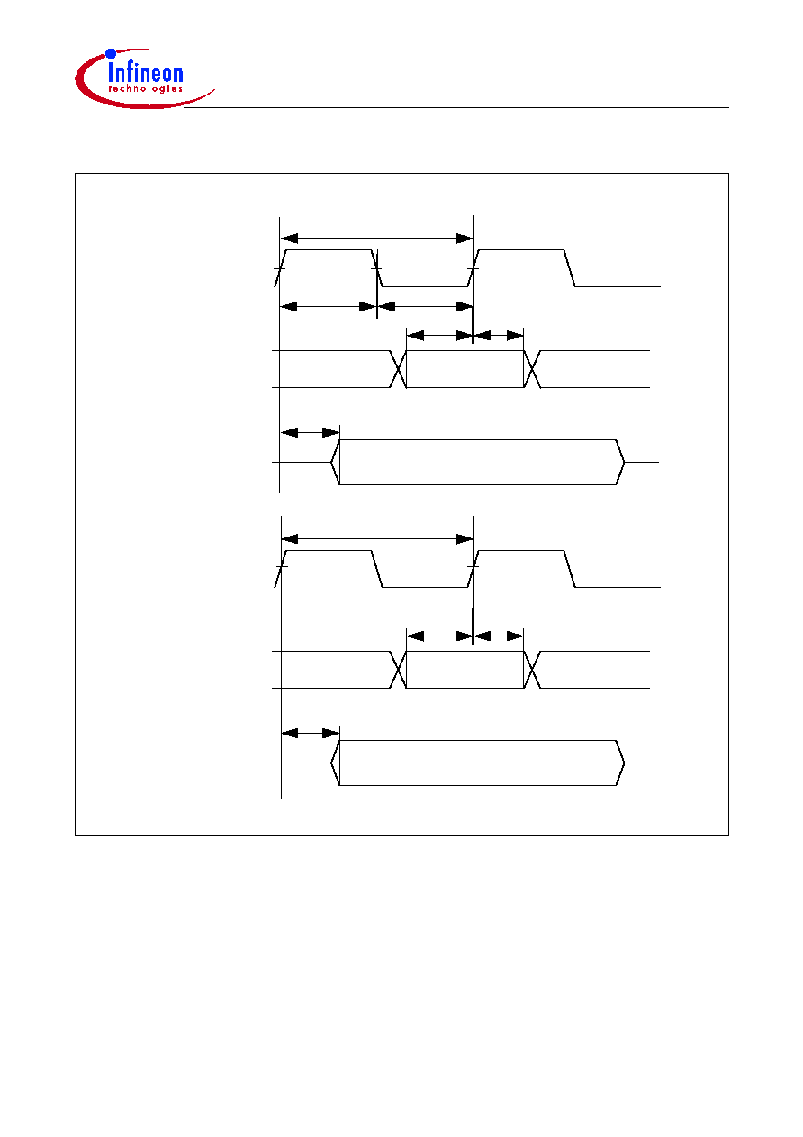
TC11IB
Data Sheet
91
V2.3, 2003-11
Figure 33
Ethernet Timing
t
1
ETXCLK
ERXCLK
ERXD(3:0)
ERXDV
ERXER
t
4
t
5
valid data
ETXD(3:0)
ETXEN
ETXER
t
6
valid data
t
7
EMDC
EMDIO
(sourced by
STA)
t
8
t
9
valid data
t
10
EMDIO
(sourced by
PHY)
valid data
t
2
t
3

TC11IB
Data Sheet
92
V2.3, 2003-11
Timing for MultiMediaCard Interface Signals
(Operating Conditions apply; C
L
= 50 pF)
Figure 34
MultiMediaCard Interface Timing
Parameter
Symbol
Limits
Unit
min
max
MMCI.CLK period
t
1
CC 62.5
-
ns
MMCI.CLK high time
t
2
CC 28
-
ns
MMCI.CLK low time
t
3
CC 28
-
ns
MMCI.CMD_RW output valid from MMCI.CLK
t
4
CC
-
4.0
ns
MMCI.DAT_RW output valid from MMCI.CLK
t
4
CC
-
3.0
ns
MMCI.ROD output valid from MMCI.CLK
t
4
CC
-
4.0
ns
MMCI.VDDEN output valid from MMCI.CLK
t
4
CC
-
2.0
ns
MMCI.CMD output valid from MMCI.CLK
t
4
CC
-
33
ns
MMCI.DAT output valid from MMCI.CLK
t
4
CC
-
33
ns
MMCI.CMD input setup to MMCI.CLK
t
5
SR 12
-
ns
MMCI.DAT input setup to MMCI.CLK
t
5
SR 10
-
ns
MMCI.CMD input hold from MMCI.CLK
t
6
SR
-
2.0
ns
MMCI.DAT input hold from MMCI.CLK
t
6
SR
-
2.0
ns
MMCI.CLK
t
1
t
2
t
3
Input
t
5
valid data
t
6
valid data
t
4
Output

TC11IB
Data Sheet
93
V2.3, 2003-11
SSC Master Mode Timing
(Operating Conditions apply; C
L
= 50 pF)
Figure 35
SSC Master Mode Timing
Parameter
Symbol
Limit Values
Unit
min.
max.
SCLK clock frequency
1 / t
SCLK
CC
-
24
MHz
SCLK clock high time
t
1
CC
18
-
ns
SCLK clock low time
t
2
CC
18
-
ns
SCLK clock rise time
t
3
CC
-
11
ns
SCLK clock fall time
t
4
CC
-
11
ns
MTSR low/high from SCLK edge
t
5
CC
-
2.0
ns
MRST setup to SCLK edge
t
6
SR
13
-
ns
MRST hold from SCLK edge
t
7
SR
7.5
-
ns
(CON.PO,CON.PH = 00 or 11)
0.9 V
DD
0.1 V
DD
t
1
t
2
t
SCLK
t
3
t
4
Data valid
Data valid
t
2
t
1
t
5
State n-1
State n
State n+1
0.9 V
DD
0.1 V
DD
t
3
t
4
t
6
t
7
SCLK
(CON.PO,CON.PH = 01 or 10)
SCLK
MTSR
MRST
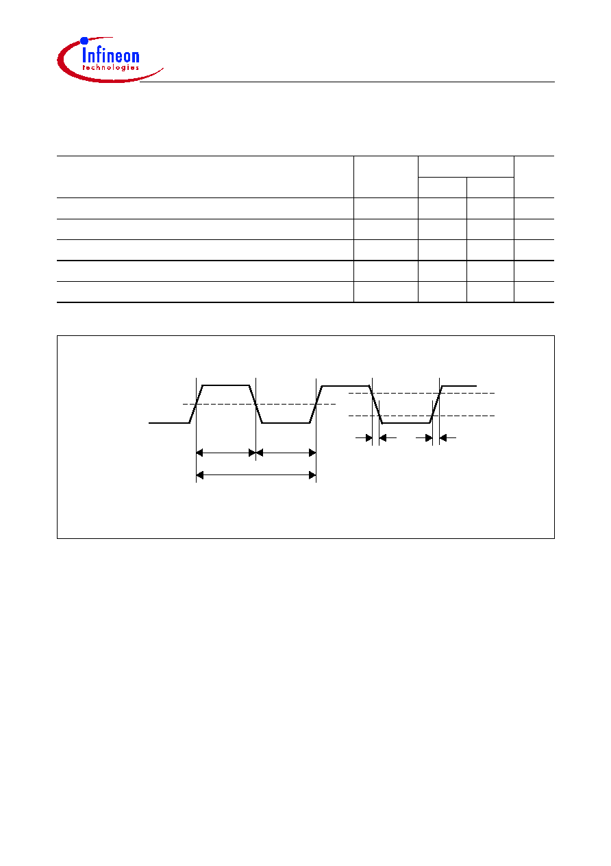
TC11IB
Data Sheet
94
V2.3, 2003-11
Timing for JTAG Signals
(Operating Conditions apply; C
L
= 50 pF)
Figure 36
TCK Clock Timing
Parameter
Symbol
Limits
Unit
min
max
TCK clock period
t
TCK
CC
50
-
ns
TCK high time
t
1
CC
10
-
ns
TCK low time
t
2
CC
29
-
ns
TCK clock rise time
t
3
CC
-
0.4
ns
TCK clock fall time
t
4
CC
-
0.4
ns
TCK
t
4
0.9 V
DD
t
3
t
1
0.1 V
DD
t
2
t
TCK
0.5 V
DD
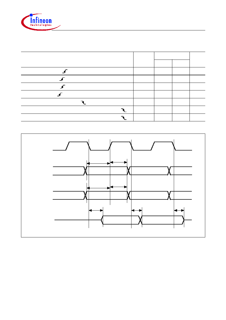
TC11IB
Data Sheet
95
V2.3, 2003-11
Figure 37
JTAG Timing
Parameter
Symbol
Limits
Unit
min
max
TMS setup to TCK
t
1
CC 7.85
-
ns
TMS hold to TCK
t
2
CC
-
1.0
ns
TDI setup to TCK
t
1
CC 10.9
-
ns
TDI hold to TCK
t
2
CC
-
1.0
ns
TDO valid output from TCK
t
3
CC
-
29.0
ns
TDO high impedance to valid output from TCK
t
4
CC
-
23.0
ns
TDO valid output to high impedance from TCK
t
5
CC
-
26.0
ns
TMS
TDI
TCK
TDO
t
1
t
2
t
1
t
2
t
4
t
3
t
5
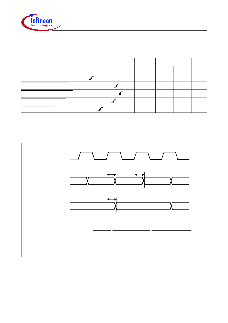
TC11IB
Data Sheet
96
V2.3, 2003-11
Timing for OCDS Trace and Breakpoint Signals
(Operating Conditions apply; C
L
= 50 pF)
Figure 38
OCDS Trace Signals Timing
Parameter
Symbol
Limits
Unit
min
max
BRK_OUT valid from CPUCLK
t
1
CC
-
17.0
ns
OCDS2_STATUS[4:0] valid from CPUCLK
t
1
CC
-
7.0
ns
OCDS2_INDIR_PC[7:0] valid from CPUCLK
t
1
CC
-
7.0
ns
OCDS2_BRKPT[2:0] valid from CPUCLK
t
1
CC
-
7.0
ns
PCP_PC[15:0] valid from CPUCLK
1)
1)
PCP Trace signals are output with respect to the slow FPI clock at 48MHz. The CPUCLK is used as a reference
here since the slow FPI clock is not available as an external pin. PCP Trace signals maintain its state for at
least 2 CPU clocks.
t
2
CC
-
7.0
ns
CPU
Trace Signals
CPUCLK
t
1
Old State
New State
Old State
New State
t
1
t
2
PCP
Trace Signals
Note:
CPU Trace Signals include BRK_OUT, OCDS2_STATUS[4:0], OCDS2_INDIR_PC[7:0]
and OCDS_BRKPT[2:0].
PCP Trace Signals include PCP_PC[15:0].

TC11IB
Data Sheet
97
V2.3, 2003-11
PCI 33MHz, 3.3V Signaling
(Operating Conditions apply; C
L
= 10 pF)
Parameter
Symbol Min.
Max.
Units Test condition
Switching Current
High
I
OH
(AC) -12V
DDP
mA
0 < V
OUT
0.3V
DDP
1)
1)
Refer to the V/I curves in
Figure 39
. Switching current characteristics for REQ and GNT are permitted to be
one half of that specified here; i.e., half size output drivers may be used on these signals. This specification
does not apply to CLK and RST which are system outputs. "Switching Current High" specifications are not
relevant to SERR, PME, INTA, INTB which are open drain outputs.
-17.1(V
DDP
-
V
OUT
)
mA
0.3V
DDP
< V
OUT
<
0.9V
DDP
1)
Eqt'n 1
2)
2)
Equation 1: I
OH
= (98/V
DDP
) . (V
OUT
- V
DDP
) . (V
OUT
+ 0.4 V
DDP
), where 0.7 V
DDP
< V
OUT
< V
DDP
0.7V
DDP
< V
OUT
<
V
DDP
1) 3)
(Test Point)
-
32V
DDP
mA
V
OUT
= 0.7V
DDP
3)
3)
Maximum current requirements must be met as drivers pull beyond the first step voltage. Equations defining
these maximums (1 and 2) are provided with the respective diagrams in
Figure 40
. The equation-defined
maximums should be met by design. In order to facilitate testing, a maximum current test point is defined for
each side of the output driver.
Switching Current
Low
I
OL
(AC) 16V
DDP
mA
V
DDP
> V
OUT
0.6V
DDP
1)
26.7V
OUT
mA
0.6V
DDP
> V
OUT
>
0.1V
DDP
1)
Eqt'n 2
4)
4)
Equation 2: I
OL
= (256/V
DDP
) . (V
OUT
) . (V
DDP
- V
OUT
), where 0 < V
OUT
< 0.18 V
DDP
0.18V
DDP
> V
OUT
> 0
1) 3)
(Test Point)
38V
DDP
mA
V
OUT
= 0.18V
DDP
3)
Low Clamp
Current
I
CL
-25 +
(V
IN
+ 1)/(0.015)
mA
-3 < V
IN
-1
High Clamp
Current
I
CH
25 +
(V
IN
- V
DDP
-1)/
(0.015)
mA
V
DDP
+4 > V
IN
V
DDP
+1
Output Rise Slew
Rate
slew
r
1
4
V / ns 0.2V
DDP
- 0.6V
DDP
load
5)
Output Fall Slew
Rate
slew
f
1
4
V / ns 0.6V
DDP
- 0.2V
DDP
load
5)
TC11IB
Data Sheet
98
V2.3, 2003-11
Figure 39
V/I Curves for 3.3V Signaling
Figure 40
Maximum AC Waveforms for 3.3V Signaling
5)
This parameter is to be interpreted as the cumulative edge rate across the specified range, rather than the
instantaneous rate at any point within the transition edge. The specified load (see
Figure 41
) is optional; i.e.,
the designer may choose to meet this parameter with an unloaded output as per revision 2.0 of the PCI Local
Bus Specification. However, adherence to both max. and min. parameters is required. Rise slew rates does
not apply to open drain outputs.
0.5V
DDP
DC
Drive point
0.1V
DDP
0.6V
DDP
Test point
1.5
16V
DDP
64V
DDP
Current (mA)
V
o
l
t
ag
e (
V
)
I
OH
= (98/V
DDP
) * (V
OUT
- V
DDP
) * (V
OUT
+ 0.4V
DDP
)
where, V
DDP
> V
OUT
> 0.7V
DDP
AC
drive point
- 0.5
- 12V
DDP
- 48V
DDP
0.3V
DDP
0.9V
DDP
V
DDP
Test
point
DC
Drive point
Current (mA)
V
o
l
t
age
(
V
)
V
DDP
I
OL
= (256/V
DDP
) * V
OUT
* (V
DDP
- V
OUT
)
where, 0 < V
OUT
< 0.18V
DDP
Pull Up
Pull Down
AC
drive point
Input
Buffer
3.3V Supply
V
R
Evaluation Setup
11ns (min)
4ns (max)
+ 7.1V
- 3.5V
0V
+ 3.6V
7.1V p-to-p
(minimum)
7.1V p-to-p
(minimum)
62.5ns (16MHz)
Overvoltage Waveform
Voltage Source Impedence
R = 29
Undervoltage Waveform
Voltage Source Impedence
R = 28
TC11IB
Data Sheet
99
V2.3, 2003-11
Figure 41
Load Circuit for Slew Rate Measurement
PCI Clock Specification
(Operating Conditions apply; C
L
= 10 pF)
Figure 42
Clock Specification
Parameter
Symbol Min.
Max.
Units Notes
CLK Cycle Time
t
CYC
30
-
ns
1)
1)
In general, the PCI component must work with any clock frequency between nominal DC and 33 MHz. Device
operational parameters at frequencies under 16 MHz may be guaranteed by design rather than by testing. The
clock frequency may be changed at any time during the operation of the system so long as the clock edges
remain "clean" (monotonic) and the minimum cycle, high and low times are not violated. The clock may only
be stopped in a low state.
CLK High Time
t
HIGH
11
-
ns
CLK Low Time
t
LOW
11
-
ns
CLK Slew Rate
-
1
4
V/ns
2)
2)
Rise and fall times are specified in terms of the edge rate measured in V/ns. This slew rate must be met across
the minimum peak-to-peak portion of the clock waveform as shown in
Figure 42
.
output buffer
pin
1/2 in. max.
10pF
1K
V
DDP
1K
0.6 V
DDP
0.2 V
DDP
0.3 V
DDP
0.4 V
DDP
0.5 V
DDP
0.4V
DDP
p-to-p (min)
t
HIGH
t
LOW
TC11IB
Data Sheet
100
V2.3, 2003-11
PCI 3.3V Timing Parameters
(
Operating Conditions apply; C
L
= 10 pF
)
Parameter
Symbol
Min.
Max.
Units
Notes
CLK to signal valid delay
- bused signals
t
VAL
2
11
ns
1)
2)
3)
1)
Refer to
Figure 43
.
2)
Minimum times are evaluated with same load used for slew rate measurement (as shown in
Figure 41
).
Maximum times are evaluated with the load circuits as illustrated in
Figure 45
.
3)
REQ and GNT are point to point signals and have different output valid delay and input setup times compared
to bused signals. GNT has a setup of 10 and REQ has a setup of 12. All other signals are bused.
CLK to signal valid delay
- point to point
t
VAL(PTP)
2
12
ns
1)
2)
3)
Float to active delay
t
ON
2
ns
1)
4)
4)
For purposes of Active/Float timing measurements, the Hi-Z or "OFF" state is defined to be when the total
current delivered through the component pin is less than or equal to the leakage current specification.
Active to Float delay
t
OFF
28
ns
1)
4)
Input setup time to CLK
- bused signals
t
SU
7
ns
3)
5)
6)
5)
Refer to
Figure 44
.
6)
Setup time applies only when the device is not driving the pin. Devices cannot drive and receive signals at the
same time.
Input setup time to CLK
- point to point
t
SU(PTP)
10, 12
ns
3)
5)
Input hold time from CLK
t
H
0
ns
5)
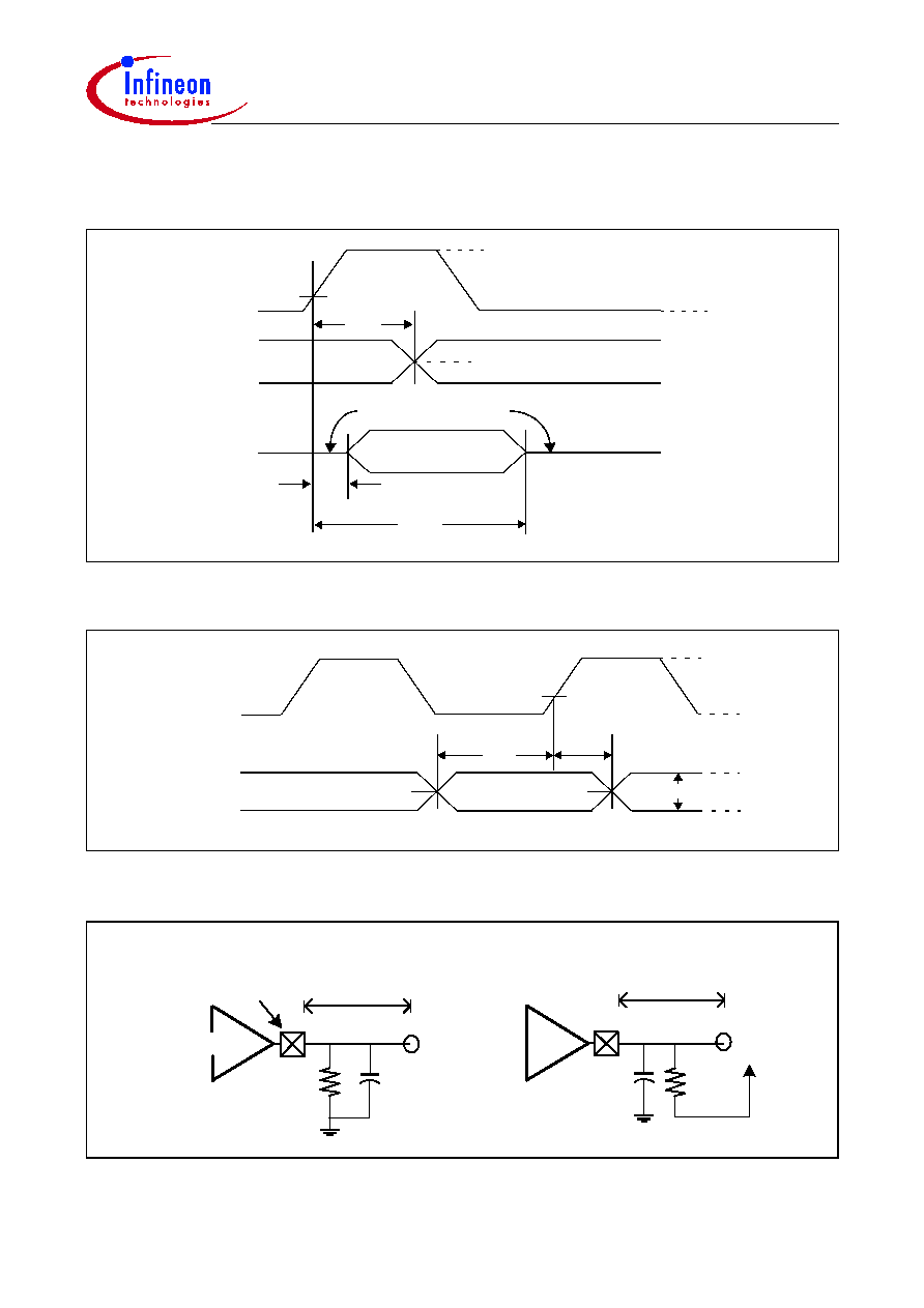
TC11IB
Data Sheet
101
V2.3, 2003-11
Measurement Conditions
Figure 43
Output timing measurement conditions
Figure 44
Input timing measurement conditions
Figure 45
Load circuits for Maximum Clock to Signal Valid Delays
CLK
Output
Delay
Tri-state
Output
V
TEST
V
TH
V
TL
t
VAL
V
STEP
t
ON
t
OFF
output current
leakage current
CLK
V
TH
V
TL
t
SU
INPUT
V
TEST
V
TH
V
TL
V
MAX
V
TEST
inputs
valid V
TEST
t
H
output buffer
pin
1/2 in. max.
10pF
25
25
10pF
1/2 in. max.
V
DDP
Tval(max) Rising Edge
Tval(max) Falling Edge
TC11IB
Data Sheet
102
V2.3, 2003-11
Parameters for Measurement Conditions
Symbol
Value
Units
Notes
V
TH
0.6 V
DDP
V
1)
1)
The input test is done with 0.1
V
DDP
overdrive. Timing parameters must be met with no more
overdrive than this.
V
TL
0.2 V
DDP
V
1)
V
TEST
0.4 V
DDP
V
V
STEP
(rising edge)
0.285 V
DDP
V
V
STEP
(falling edge)
0.615 V
DDP
V
V
MAX
0.4 V
DDP
V
2)
2)
V
MAX
specifies the maximum peak-to-peak waveform allowed for measuring input timing.
Production testing may use different voltage values, but must correlate results back to these
parameters.
Input signal edge rate
1
V / ns
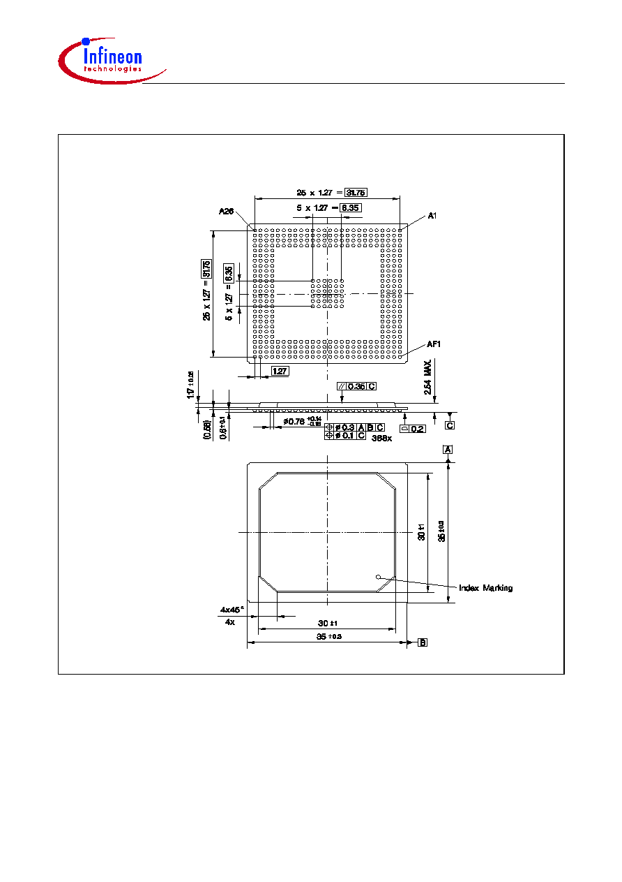
TC11IB
Data Sheet
103
V2.3, 2003-11
Package Outline
Figure 46
P-BGA-388-2 Package
Sorts of Packing
Package outlines for tubes, trays, etc. are contained in Data Sheet "Package
Information"
SMD = Surface Mounted Device
Plastic Package, P-BGA-388-2 (SMD)
(Plastic Ball Grid Array Package)

h t t p : / / w w w . i n f i n e o n . c o m
Published by Infineon Technologies AG
Infineon goes for Business Excellence
"Business excellence means intelligent approaches and clearly
defined processes, which are both constantly under review and
ultimately lead to good operating results.
Better operating results and business excellence mean less
idleness and wastefulness for all of us, more professional
success, more accurate information, a better overview and,
thereby, less frustration and more satisfaction."
Dr. Ulrich Schumacher