Äîêóìåíòàöèÿ è îïèñàíèÿ www.docs.chipfind.ru
IPD13N03LA IPF13N03LA
IPS13N03LA IPU13N03LA
Opti
MOS
®
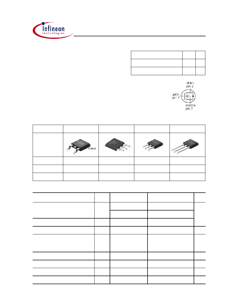
2 Power-Transistor
Features
· Ideal for high-frequency dc/dc converters
· Qualified according to JEDEC
1)
for target applications
· N-channel, logic level
· Excellent gate charge x R
DS(on)
product (FOM)
· Superior thermal resistance
· 175 °C operating temperature
Maximum ratings, at T
j
=25 °C, unless otherwise specified
Parameter
Symbol Conditions
Unit
Continuous drain current
I
D
T
C
=25 °C
2)
30
A
T
C
=100 °C
30
Pulsed drain current
I
D,pulse
T
C
=25 °C
3)
210
Avalanche energy, single pulse
E
AS
I
D
=24 A, R
GS
=25
60
mJ
Reverse diode dv /dt
dv /dt
I
D
=30 A, V
DS
=20 V,
di /dt =200 A/µs,
T
j,max
=175 °C
6
kV/µs
Gate source voltage
4)
V
GS
±20
V
Power dissipation
P
tot
T
C
=25 °C
46
W
Operating and storage temperature
T
j
, T
stg
-55 ... 175
°C
IEC climatic category; DIN IEC 68-1
55/175/56
Value
V
DS
25
V
R
DS(on),max
12.8
m
I
D
30
A
Product Summary
Type
IPD13N03LA
IPF13N03LA
IPS13N03LA
IPU13N03LA
Package
P-TO252-3-11
P-TO252-3-23
P-TO251-3-11
P-TO251-3-21
Ordering Code
Q67042-S4159
Q67042-S4195
Q67042-S4248
Q67042-S4160
Marking
13N03LA
13N03LA
13N03LA
13N03LA
Rev. 1.7
page 1
2004-05-24
IPD13N03LA IPF13N03LA
IPS13N03LA IPU13N03LA
Parameter
Symbol Conditions
Unit
min.
typ.
max.
Thermal characteristics
Thermal resistance, junction - case
R
thJC
-
-
3.2
K/W
SMD version, device on PCB
R
thJA
minimal footprint
-
-
75
6 cm
2
cooling area
5)
-
-
50
Electrical characteristics, at T
j
=25 °C, unless otherwise specified
Static characteristics
Drain-source breakdown voltage
V
(BR)DSS
V
GS
=0 V, I
D
=1 mA
25
-
-
V
Gate threshold voltage
V
GS(th)
V
DS
=V
GS
, I
D
=20 µA
1.2
1.6
2
Zero gate voltage drain current
I
DSS
V
DS
=25 V, V
GS
=0 V,
T
j
=25 °C
-
0.1
1
µA
V
DS
=25 V, V
GS
=0 V,
T
j
=125 °C
-
10
100
Gate-source leakage current
I
GSS
V
GS
=20 V, V
DS
=0 V
-
10
100
nA
Drain-source on-state resistance
R
DS(on)
V
GS
=4.5 V, I
D
=20 A
-
17.5
21.9
m
V
GS
=10 V, I
D
=30 A
-
10.7
12.8
Gate resistance
R
G
-
0.9
-
Transconductance
g
fs
|V
DS
|>2|I
D
|R
DS(on)max
,
I
D
=30 A
18
36
-
S
5)
Device on 40 mm x 40 mm x 1.5 mm epoxy PCB FR4 with 6 cm
2
(one layer, 70 µm thick) copper area for drain
connection. PCB is vertical in still air.
Values
2)
Current is limited by bondwire; with an R
thJC
=3.2 K/W the chip is able to carry 47 A.
3)
See figure 3
4)
T
j,max
=150 °C and duty cycle D <0.25 for V
GS
<-5 V
1)
J-STD20 and JESD22
Rev. 1.7
page 2
2004-05-24
IPD13N03LA IPF13N03LA
IPS13N03LA IPU13N03LA
Parameter
Symbol Conditions
Unit
min.
typ.
max.
Dynamic characteristics
Input capacitance
C
iss
-
784
1043
pF
Output capacitance
C
oss
-
303
402
Reverse transfer capacitance
C
rss
-
41
62
Turn-on delay time
t
d(on)
-
5.4
8.0
ns
Rise time
t
r
-
4.6
6.9
Turn-off delay time
t
d(off)
-
15
23
Fall time
t
f
-
2.6
3.9
Gate Charge Characteristics
6)
Gate to source charge
Q
gs
-
2.7
3.6
nC
Gate charge at threshold
Q
g(th)
-
1.3
1.7
Gate to drain charge
Q
gd
-
1.8
2.7
Switching charge
Q
sw
-
3.3
4.7
Gate charge total
Q
g
-
6.3
8.3
Gate plateau voltage
V
plateau
-
3.4
-
V
Gate charge total, sync. FET
Q
g(sync)
V
DS
=0.1 V,
V
GS
=0 to 5 V
-
5.5
7.3
nC
Output charge
Q
oss
V
DD
=15 V, V
GS
=0 V
-
6.6
8.7
Reverse Diode
Diode continous forward current
I
S
-
-
30
A
Diode pulse current
I
S,pulse
-
-
210
Diode forward voltage
V
SD
V
GS
=0 V, I
F
=30 A,
T
j
=25 °C
-
0.95
1.2
V
Reverse recovery charge
Q
rr
V
R
=15 V, I
F
=I
S
,
di
F
/dt =400 A/µs
-
-
10
nC
6)
See figure 16 for gate charge parameter definition
T
C
=25 °C
Values
V
GS
=0 V, V
DS
=15 V,
f =1 MHz
V
DD
=15 V, V
GS
=10 V,
I
D
=15 A, R
G
=2.7
V
DD
=15 V, I
D
=15 A,
V
GS
=0 to 5 V
Rev. 1.7
page 3
2004-05-24
IPD13N03LA IPF13N03LA
IPS13N03LA IPU13N03LA
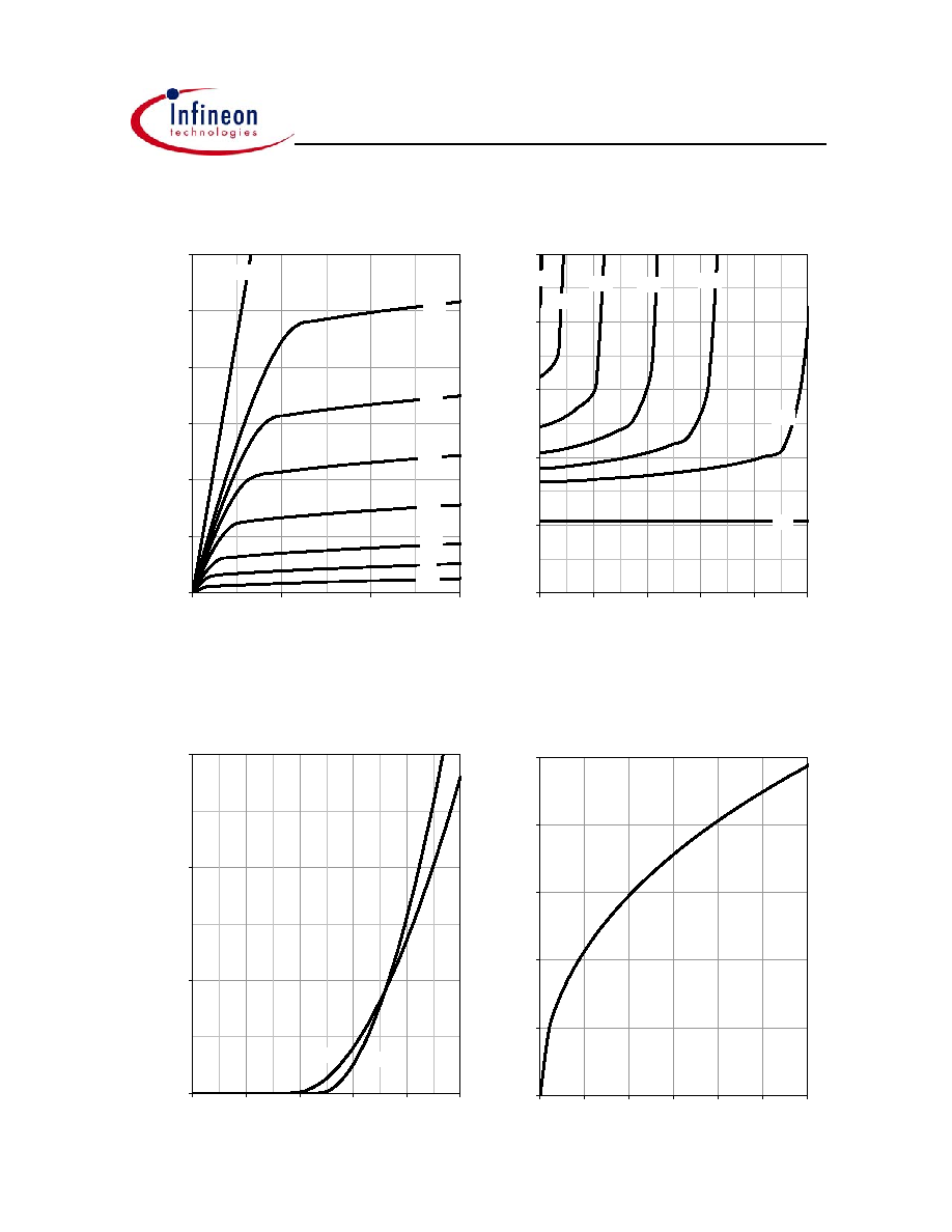
1 Power dissipation
2 Drain current
P
tot
=f(T
C
)
I
D
=f(T
C
); V
GS
10 V
3 Safe operating area
4 Max. transient thermal impedance
I
D
=f(V
DS
); T
C
=25 °C; D =0
Z
thJC
=f(t
p
)
parameter: t
p
parameter: D =t
p
/T
1 µs
10 µs
100 µs
1 ms
10 ms
DC
1
10
100
1000
0.1
1
10
100
V
DS
[V]
I
D
[A]
limited by on-state
resistance
single pulse
0.01
0.02
0.05
0.1
0.2
0.5
10
0
10
-1
10
-2
10
-3
10
-4
10
-5
10
-6
0.01
0.1
1
10
0
0
0
0
0
0
1
t
p
[s]
Z
thJ
C
[K/W]
0
10
20
30
40
50
0
50
100
150
200
T
C
[°C]
P
tot
[W]
0
10
20
30
40
0
50
100
150
200
T
C
[°C]
I
D
[A]
Rev. 1.7
page 4
2004-05-24
IPD13N03LA IPF13N03LA
IPS13N03LA IPU13N03LA
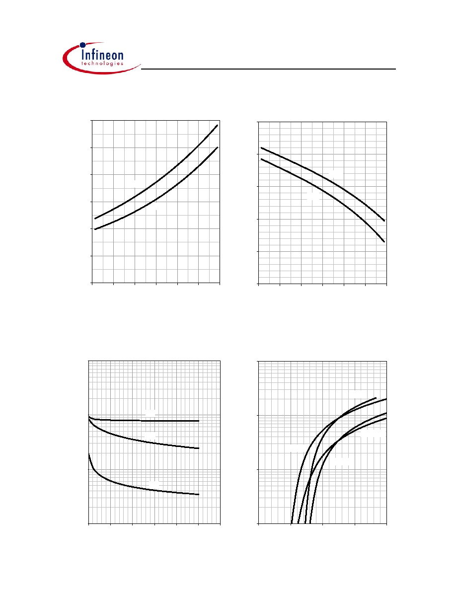
5 Typ. output characteristics
6 Typ. drain-source on resistance
I
D
=f(V
DS
); T
j
=25 °C
R
DS(on)
=f(I
D
); T
j
=25 °C
parameter: V
GS
parameter: V
GS
7 Typ. transfer characteristics
8 Typ. forward transconductance
I
D
=f(V
GS
); |V
DS
|>2|I
D
|R
DS(on)max
g
fs
=f(I
D
); T
j
=25 °C
parameter: T
j
3 V
3.2 V
3.5 V
3.8 V
4.1 V
4.5 V
10 V
0
10
20
30
40
50
0
10
20
30
40
50
I
D
[A]
R
DS
(on)
[m
]
25 °C
175 °C
0
20
40
60
0
1
2
3
4
5
V
GS
[V]
I
D
[A]
0
10
20
30
40
50
0
10
20
30
40
50
60
I
D
[A]
g
fs
[S]
2.8 V
3 V
3.2 V
3.5 V
3.8 V
4.1 V
4.5 V
10 V
0
10
20
30
40
50
60
0
1
2
3
V
DS
[V]
I
D
[A]
Rev. 1.7
page 5
2004-05-24
IPD13N03LA IPF13N03LA
IPS13N03LA IPU13N03LA
9 Drain-source on-state resistance
10 Typ. gate threshold voltage
R
DS(on)
=f(T
j
); I
D
=30 A; V
GS
=10 V
V
GS(th)
=f(T
j
); V
GS
=V
DS
parameter: I
D
11 Typ. Capacitances
12 Forward characteristics of reverse diode
C =f(V
DS
); V
GS
=0 V; f =1 MHz
I
F
=f(V
SD
)
parameter: T
j
typ
98 %
0
4
8
12
16
20
24
-60
-20
20
60
100
140
180
T
j
[°C]
R
DS
(on)
[m
]
20 µA
200 µA
0
0.5
1
1.5
2
2.5
-60
-20
20
60
100
140
180
T
j
[°C]
V
G
S
(th)
[V]
Ciss
Coss
Crss
10
4
10
3
10
2
10
1
10
100
1000
10000
0
5
10
15
20
25
30
V
DS
[V]
C
[pF]
25 °C
175 °C
25 °C, 98%
175 °C, 98%
1
10
100
1000
0.0
0.5
1.0
1.5
2.0
V
SD
[V]
I
F
[A]
Rev. 1.7
page 6
2004-05-24
IPD13N03LA IPF13N03LA
IPS13N03LA IPU13N03LA
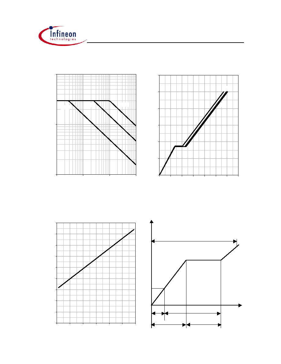
13 Avalanche characteristics
14 Typ. gate charge
I
AS
=f(t
AV
); R
GS
=25
V
GS
=f(Q
gate
); I
D
=25 A pulsed
parameter: T
j(start)
parameter: V
DD
15 Drain-source breakdown voltage
16 Gate charge waveforms
V
BR(DSS)
=f(T
j
); I
D
=1 mA
5 V
15 V
20 V
0
2
4
6
8
10
12
0
2
4
6
8
10
12
14
Q
gate
[nC]
V
GS
[V]
20
21
22
23
24
25
26
27
28
29
-60
-20
20
60
100
140
180
T
j
[°C]
V
BR(DS
S
)
[V]
V
GS
Q
gate
V
g s(th)
Q
g(th)
Q
g s
Q
g d
Q
sw
Q
g
25 °C
100 °C
150 °C
1
10
100
1
10
100
1000
t
AV
[µs]
I
AV
[A]
Rev. 1.7
page 7
2004-05-24
IPD13N03LA IPF13N03LA
IPS13N03LA IPU13N03LA
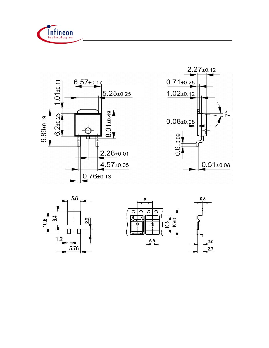
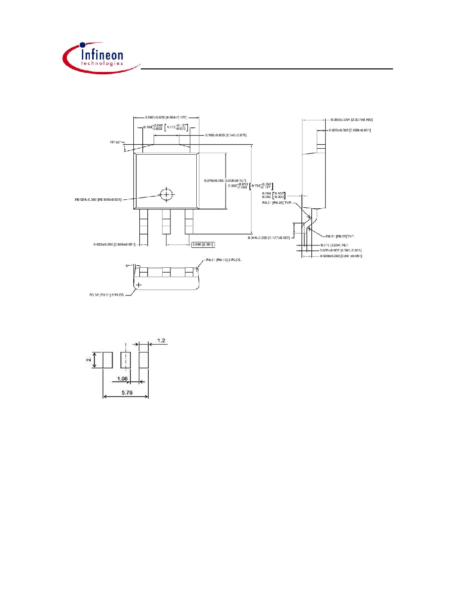
Package Outline
P-TO252-3-11: Outline
Footprint:
Packaging:
Dimensions in mm
Rev. 1.7
page 8
2004-05-24
IPD13N03LA IPF13N03LA
IPS13N03LA IPU13N03LA
Package Outline
P-TO252-3-23: Outline
Footprint:
Dimensions in inch [mm]
Rev. 1.7
page 9
2004-05-24
IPD13N03LA IPF13N03LA
IPS13N03LA IPU13N03LA
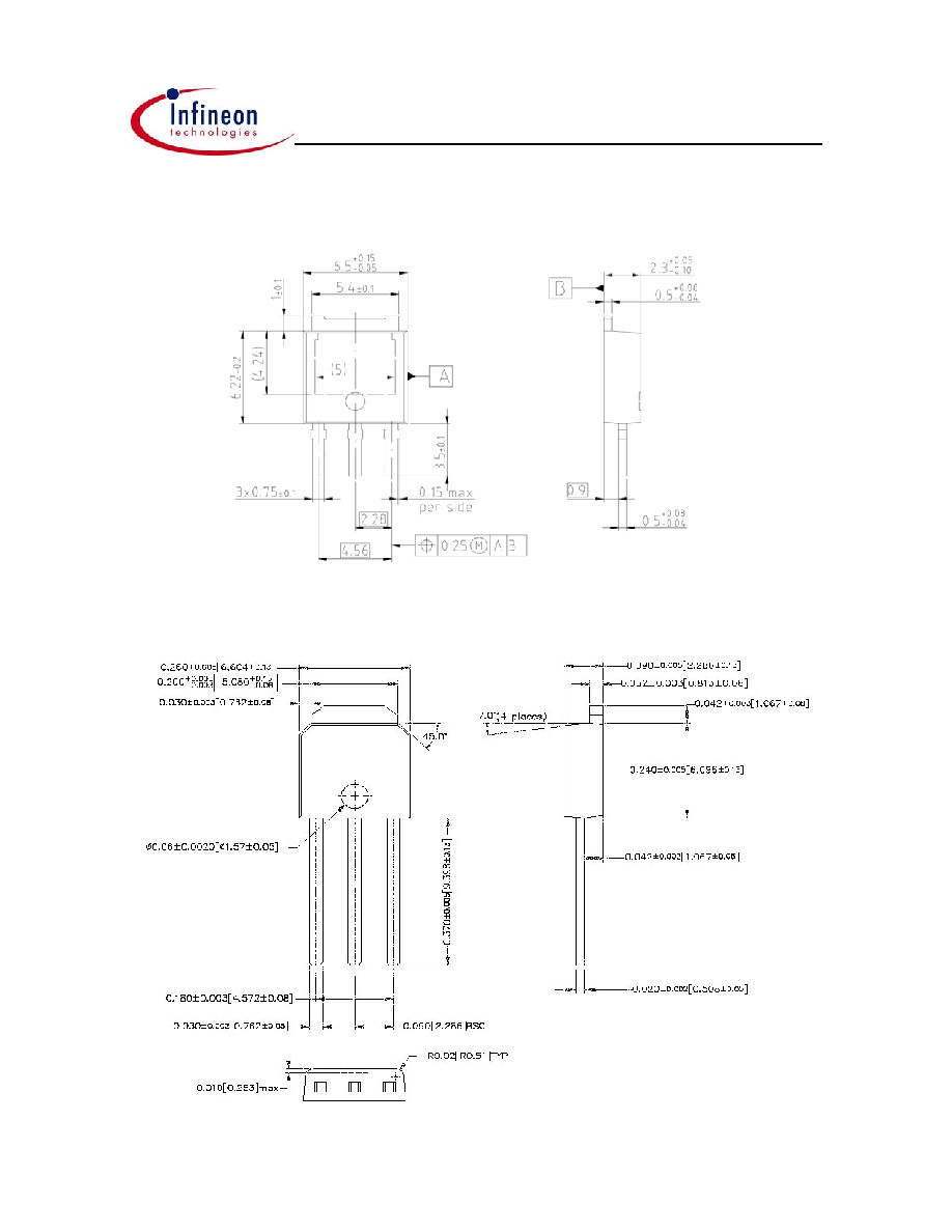
Package Outline
P-TO251-3-11: Outline
P-TO251-3-21: Outline
Dimensions in inch [mm]
Rev. 1.7
page 10
2004-05-24

IPD13N03LA IPF13N03LA
IPS13N03LA IPU13N03LA
Published by
Infineon Technologies AG
Bereich Kommunikation
St.-Martin-Straße 53
D-81541 München
© Infineon Technologies AG 1999
All Rights Reserved.
Attention please!
The information herein is given to describe certain components and shall not be considered as
warranted characteristics.
Terms of delivery and rights to technical change reserved.
We hereby disclaim any and all warranties, including but not limited to warranties of non-infringement,
regarding circuits, descriptions and charts stated herein.
Infineon Technologies is an approved CECC manufacturer.
Information
For further information on technology, delivery terms and conditions and prices, please contact your
nearest Infineon Technologies office in Germany or our Infineon Technologies representatives worldwide
(see address list).
Warnings
Due to technical requirements, components may contain dangerous substances.
For information on the types in question, please contact your nearest Infineon Technologies office.
Infineon Technologies' components may only be used in life-support devices or systems with the
expressed written approval of Infineon Technologies if a failure of such components can reasonably
be expected to cause the failure of that life-support device or system, or to affect the safety or
effectiveness of that device or system. Life support devices or systems are intended to be implanted
in the human body, or to support and/or maintain and sustain and/or protect human life. If they fail,
it is reasonable to assume that the health of the user or other persons may be endangered.
Rev. 1.7
page 11
2004-05-24