Äîêóìåíòàöèÿ è îïèñàíèÿ www.docs.chipfind.ru
IPB60R165CP
CoolMOS
TM
Power Transistor
Features
· Lowest figure-of-merit R
ON
xQ
g
· Ultra low gate charge
· Extreme dv/dt rated
· High peak current capability
· Qualified according to JEDEC
1)
for target applications
· Pb-free lead plating; RoHS compliant
CoolMOS CP is specially designed for:
· Hard switching topologies for Server and Telecom
Maximum ratings, at T
j
=25 °C, unless otherwise specified
Parameter
Symbol Conditions
Unit
Continuous drain current
I
D
T
C
=25 °C
A
T
C
=100 °C
Pulsed drain current
2)
I
D,pulse
T
C
=25 °C
Avalanche energy, single pulse
E
AS
I
D
=7.9 A, V
DD
=50 V
522
mJ
Avalanche energy, repetitive t
AR
2),3)
E
AR
I
D
=7.9 A, V
DD
=50 V
Avalanche current, repetitive t
AR
2),3)
I
AR
A
MOSFET dv /dt ruggedness
dv /dt
V
DS
=0...480 V
V/ns
Gate source voltage
V
GS
static
V
AC (f >1 Hz)
Power dissipation
P
tot
T
C
=25 °C
W
Operating and storage temperature
T
j
, T
stg
°C
Value
21
13
61
±30
192
-55 ... 150
0.79
7.9
50
±20
V
DS
@ T
j,max
650
V
R
DS(on),max
0.165
Q
g,typ
39
nC
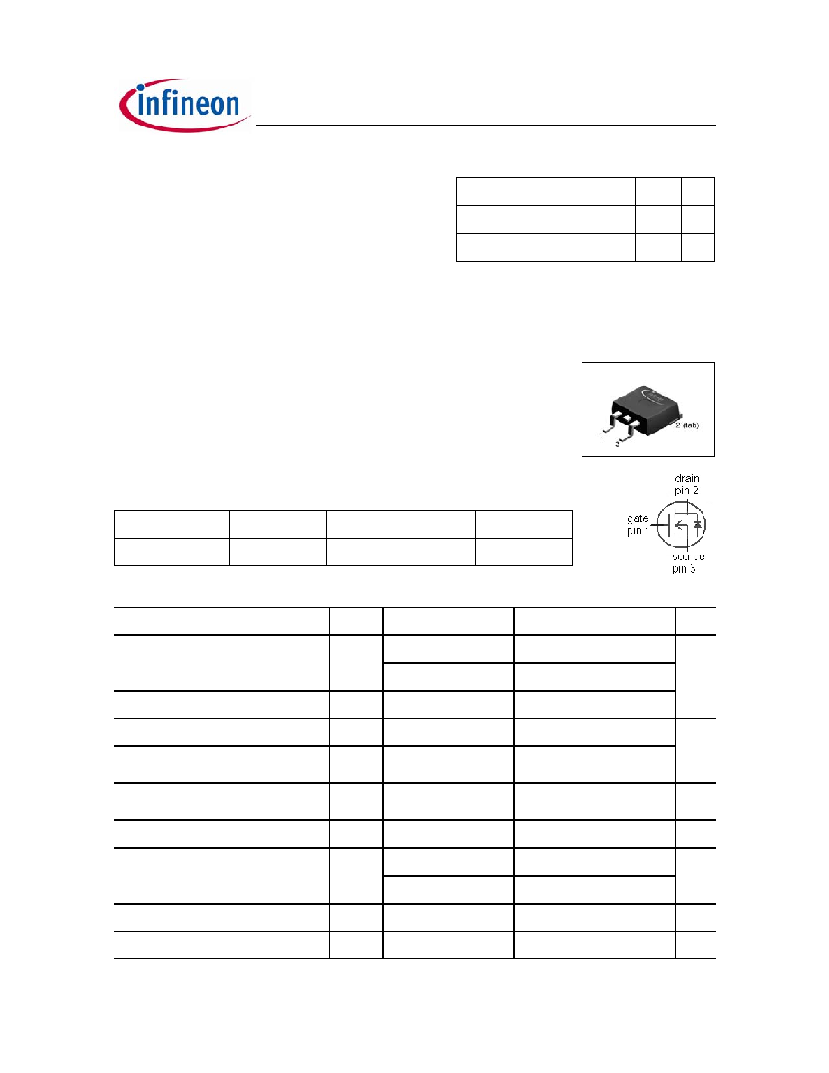
Product Summary
Type
Package
Ordering Code
Marking
IPP60R165CP
PG-TO263
SP000096439
6R165P
PG-TO263
Rev. 2.0
page 1
2006-06-19

IPB60R165CP
Maximum ratings, at T
j
=25 °C, unless otherwise specified
Parameter
Symbol Conditions
Unit
Continuous diode forward current
I
S
A
Diode pulse current
2)
I
S,pulse
61
Reverse diode dv /dt
4)
dv /dt
15
V/ns
Parameter
Symbol Conditions
Unit
min.
typ.
max.
Thermal characteristics
Thermal resistance, junction - case
R
thJC
-
-
0.65
K/W
R
thJA
SMD version, device
on PCB, minimal
footprint
-
-
62
SMD version, device
on PCB, 6 cm
2
cooling
area
5)
35
Soldering temperature,
reflowsoldering
T
sold
reflow MSL 1
-
-
260
°C
Electrical characteristics, at T
j
=25 °C, unless otherwise specified
Static characteristics
Drain-source breakdown voltage
V
(BR)DSS
V
GS
=0 V, I
D
=250 µA
600
-
-
V
Gate threshold voltage
V
GS(th)
V
DS
=V
GS
, I
D
=0.79 mA
2.5
3
3.5
Zero gate voltage drain current
I
DSS
V
DS
=600 V, V
GS
=0 V,
T
j
=25 °C
-
-
1
µA
V
DS
=600 V, V
GS
=0 V,
T
j
=150 °C
-
10
-
Gate-source leakage current
I
GSS
V
GS
=20 V, V
DS
=0 V
-
-
100
nA
Drain-source on-state resistance
R
DS(on)
V
GS
=10 V, I
D
=12 A,
T
j
=25 °C
-
0.15
0.165
V
GS
=10 V, I
D
=12 A,
T
j
=150 °C
-
0.40
-
Gate resistance
R
G
f =1 MHz, open drain
-
1.9
-
Values
Thermal resistance, junction -
ambient
Value
T
C
=25 °C
12
Rev. 2.0
page 2
2006-06-19

IPB60R165CP
Parameter
Symbol Conditions
Unit
min.
typ.
max.
Dynamic characteristics
Input capacitance
C
iss
-
2000
-
pF
Output capacitance
C
oss
-
100
-
Effective output capacitance, energy
related
6)
C
o(er)
-
83
-
Effective output capacitance, time
related
7)
C
o(tr)
-
220
-
Turn-on delay time
t
d(on)
-
12
-
ns
Rise time
t
r
-
5
-
Turn-off delay time
t
d(off)
-
50
-
Fall time
t
f
-
5
-
Gate Charge Characteristics
Gate to source charge
Q
gs
-
9
-
nC
Gate to drain charge
Q
gd
-
13.0
-
Gate charge total
Q
g
-
39
52
Gate plateau voltage
V
plateau
-
5.0
-
V
Reverse Diode
Diode forward voltage
V
SD
V
GS
=0 V, I
F
=12 A,
T
j
=25 °C
-
0.9
1.2
V
Reverse recovery time
t
rr
-
390
-
ns
Reverse recovery charge
Q
rr
-
7.5
-
µC
Peak reverse recovery current
I
rrm
-
38
-
A
1)
J-STD20 and JESD22
2)
Pulse width t
p
limited by T
j,max
Values
V
GS
=0 V, V
DS
=100 V,
f =1 MHz
V
DD
=400 V,
V
GS
=10 V, I
D
=12 A,
R
G
=3.3
V
DD
=400 V, I
D
=12 A,
V
GS
=0 to 10 V
V
GS
=0 V, V
DS
=0 V
to 480 V
7)
C
o(tr)
is a fixed capacitance that gives the same charging time as C
oss
while V
DS
is rising from 0 to 80% V
DSS.
4)
I
SD
=I
D
, di/dt<=200A/µs,V
DClink
=400V, V
peak
>V
(BR)DSS
, T
j
<T
jmax
, identical low side and high side switch.
V
R
=400 V, I
F
=I
S
,
di
F
/dt =100 A/µs
5)
Device on 40mm*40mm*1.5 epoxy PCB FR4 with 6cm2 (one layer, 70µm thick) copper area for drain connection. PCB
is vertical without blown air
6)
C
o(er)
is a fixed capacitance that gives the same stored energy as C
oss
while V
DS
is rising from 0 to 80% V
DSS.
3)
Repetitive avalanche causes additional power losses that can be calculated as P
AV
=E
AR
*f.
Rev. 2.0
page 3
2006-06-19
IPB60R165CP
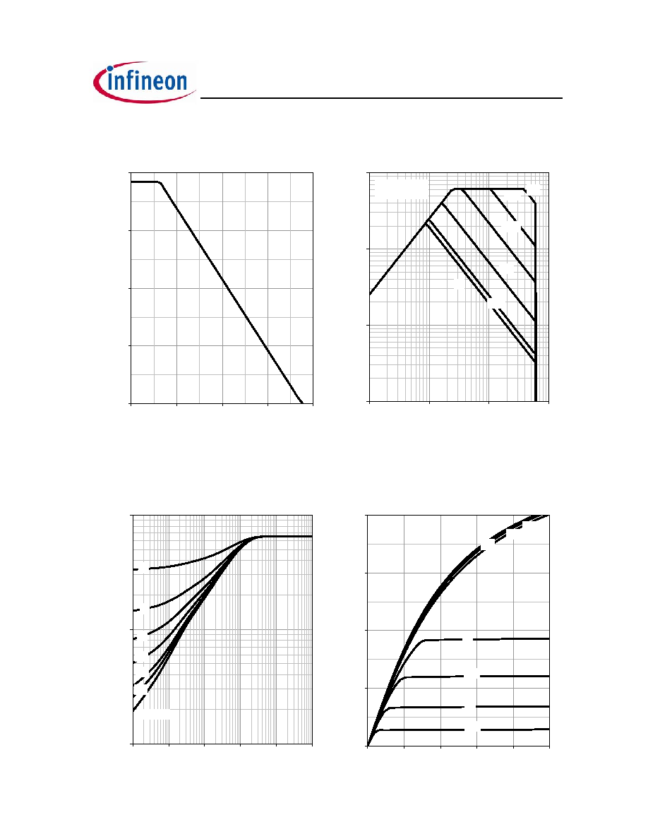
1 Power dissipation
2 Safe operating area
P
tot
=f(T
C
)
I
D
=f(V
DS
); T
C
=25 °C; D =0
parameter: t
p
3 Max. transient thermal impedance
4 Typ. output characteristics
Z
thJC
=f(t
p
)
I
D
=f(V
DS
); T
j
=25 °C
parameter: D=t
p
/T
parameter: V
GS
0
50
100
150
200
0
40
80
120
160
T
C
[°C]
P
tot
[W]
1 µs
10 µs
100 µs
1 ms
10 ms
DC
10
3
10
2
10
1
10
0
10
2
10
1
10
0
10
-1
V
DS
[V]
I
D
[A]
single pulse
0.01
0.02
0.05
0.1
0.2
0.5
10
0
10
-1
10
-2
10
-3
10
-4
10
-5
10
0
10
-1
10
-2
t
p
[s]
Z
thJ
C
[K/W]
4.5 V
5 V
5.5 V
6 V
8 V
10V
12 V
20 V
0
20
40
60
80
0
5
10
15
20
25
V
DS
[V]
I
D
[A]
limited by on-state
resistance
Rev. 2.0
page 4
2006-06-19
IPB60R165CP
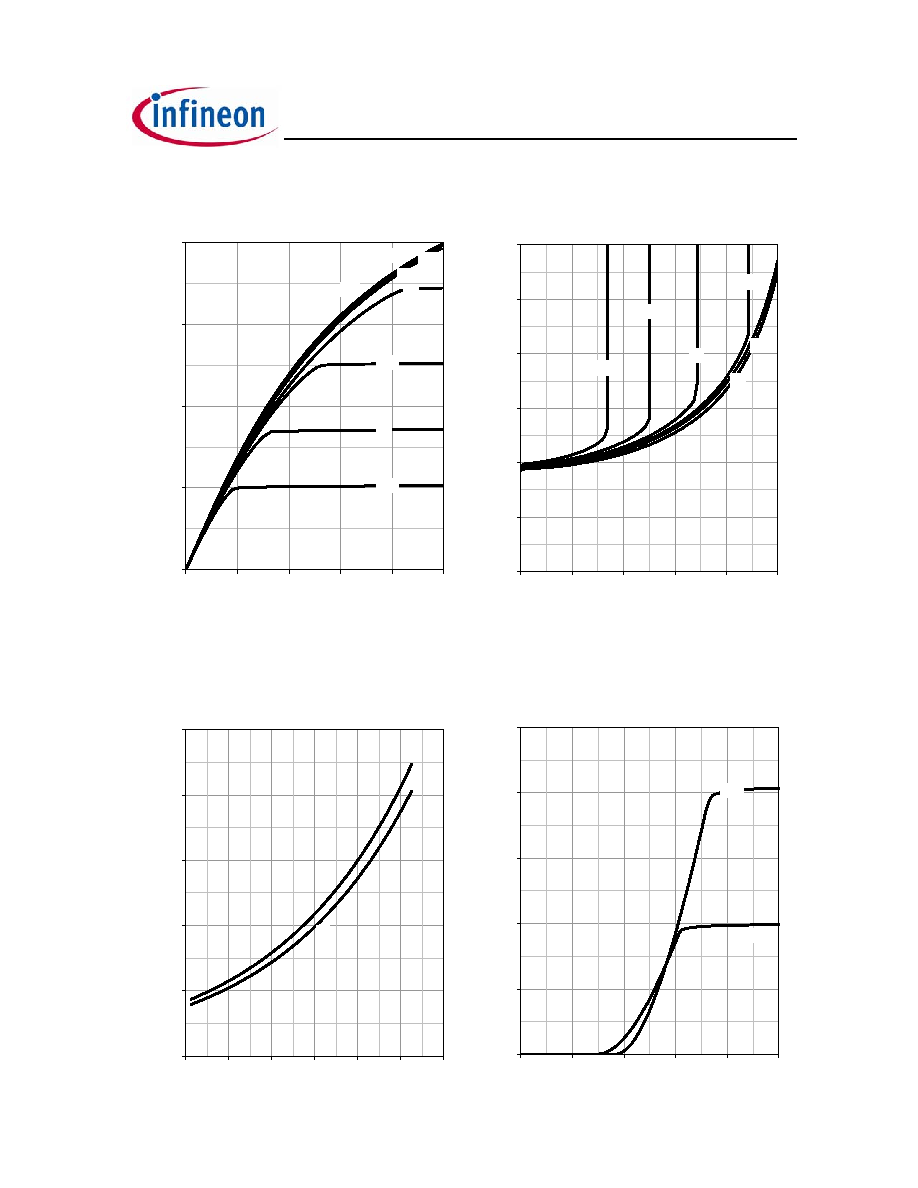
5 Typ. output characteristics
6 Typ. drain-source on-state resistance
I
D
=f(V
DS
); T
j
=150 °C
R
DS(on)
=f(I
D
); T
j
=150 °C
parameter: V
GS
parameter: V
GS
7 Drain-source on-state resistance
8 Typ. transfer characteristics
R
DS(on)
=f(T
j
); I
D
=12 A; V
GS
=10 V
I
D
=f(V
GS
); |V
DS
|>2|I
D
|R
DS(on)max
parameter: T
j
typ
98%
0
0.1
0.2
0.3
0.4
0.5
-60
-20
20
60
100
140
180
T
j
[°C]
R
DS
(on)
[
]
C °25
C °150
0
20
40
60
80
100
0
2
4
6
8
10
V
GS
[V]
I
D
[A]
4.5 V
5 V
5.5 V
6 V
8 V
10 V
12 V
20 V
0
10
20
30
40
0
5
10
15
20
25
V
DS
[V]
I
D
[A]
5 V
5.5 V
6 V
6.5 V
7 V
10 V
0
0.2
0.4
0.6
0.8
1
1.2
0
10
20
30
40
50
I
D
[A]
R
DS
(on)
[
]
Rev. 2.0
page 5
2006-06-19