Data Sheet
1
2001-01-01
GaAs MMIC
CMY 210
Data Sheet
·
Ultralinear Mixer with integrated LO-Buffer
·
Very high Input-IP3 of typical 24 dBm
·
Very low LO-Power demand of typ. 0 dBm
·
Suited for Up- and Down-Conversion
·
Wide LO-Frequency Range < 500 MHz to
> 2.5 GHz
·
Wide LO-Level Range
·
Single ended Ports
·
RF- and IF-Port Impedance 50
·
Operating Voltage Range: < 3 to 6 V
·
Very low Current Consumption of typical 6 mA
·
All Gold Metallization
ESD: Electrostatic discharge sensitive device
Observe handling Precautions!
Type
Marking
Ordering Code
(tape and reel)
Package
1)
1)
For detailed dimensions see Page 10.
CMY 210
M3
Q62702-M0016
MW-6
Maximum Ratings
Parameter
Port
Symbol
Limit Values
Unit
min.
max.
Supply Voltage
4
V
DD
0
6
V
DC-Voltage at LO Input
3
V
3
3
0.5
V
DC-Voltage at RF-IF Ports
1)
1)
For DC test purposes only, no DC voltages at pins 1, 6 in application.
1, 6
V
1, 6
0.5
+ 0.5
V
Power into RF-IF Ports
1, 6
P
IN,RF
17
dBm
Power into LO Input
3
P
IN,LO
10
dBm
Channel Temperature
T
Ch
150
°
C
Storage Temperature
T
stg
55
150
°
C
MW-6

GaAs Components
CMY 210
Data Sheet
2
2001-01-01
Thermal Resistance
Parameter
Symbol
Value
Unit
Channel to Soldering Point (GND)
R
thChS
100
K/W
Electrical Characteristics
T
A
= 25
°
C;
V
DD
= 3 V, see test circuit;
f
RF
= 808 MHz;
f
LO
= 965 MHz;
P
LO
= 0 dBm;
f
IF
= 157 MHz, unless otherwise specified.
Parameters
Symbol
Limit Values
Unit
Test
Conditions
min.
typ.
max.
Operating Current
I
OP
6.0
8.0
mA
Conversion Loss
L
C
5.7
7.0
dB
SSB Noise Figure
F
SSB
6.0
dB
2 Tone 3
rd
Order
IMD
d
IM3
54
dBc
P
RF1
= 3 dBm
P
RF2
= 3 dBm
f
RF1
= 806 MHz;
f
RF2
= 810 MHz;
f
LO
= 965 MHz
3
rd
Order Input
Intercept Point
IP3
IN
20
24
dBm
Input Power
P
1 dB
14
dBm
LO Leakage at
RF/IF-Port (1, 6)
P
LO 1, 6
8
dBm
GaAs Components
CMY 210
Data Sheet
3
2001-01-01
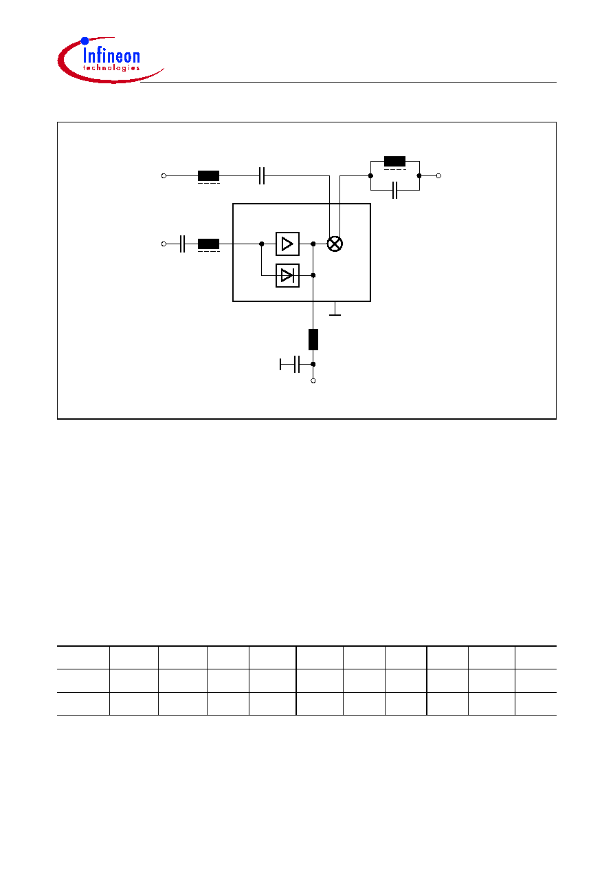
Figure 1
Test Circuit/Application Example
Notes for External Elements
L
1
,
C
1
: Filter for upper frequency.
C
2
,
L
2
: Filter for lower frequency.
Each filter is a throughpath for the desired frequency (RF or IF) and isolates the other
frequency (IF or RF) and its harmonics.
These two filters must be connected to pin 1 and pin 6 directly.
Parasitic capacitances at the ports 1 and 6 must be as small as possible.
L
4
and
C
4
are optimized by indicating lowest
I
OP
at used LO-frequency; same procedure
for
L
3
.
The ports 1, 3 and 6 must be DC open.
Lumped Element Values for 800 MHz Test and Application Circuit
f
LO
F
RF
F
IF
L
1
C
1
L
2
C
2
L
3
C
3
L
4
C
4
MHz
MHz
MHz
nH
pF
nH
pF
nH
pF
nH
pF
965
808
157
8.2
3.9
8.2
3.3
6.8
47
15
33
EHT08981
1
6
2, 5
3
4
CMY 210
LO IN
3
C
L
3
4
L
DD
V
C
4
C
1
1
L
RF
IN / OUT
50
L
2
C
2
OUT / IN
IF
50

GaAs Components
CMY 210
Data Sheet
4
2001-01-01
Figure 2
PCB-Layout for 800 MHz Test and Application Circuit
Typical Lumped Element Values for Different RF-Frequencies
f
RF
L
1
C
1
L
2
C
2
MHz
nH
pF
nH
pF
400
12
15
12
12
450
12
12
12
10
900
8.2
3.9
8.2
3.3
1500
3.3
2.7
3.3
2.2
1800
3.3
2.2
3.3
1.8
2000
3.3
1.8
3.3
1.2
2400
1.8
2.7
1.8
1.5
Typical Lumped Element Values for Different LO-Frequencies
f
LO
L
3
C
3
L
4
C
4
MHz
nH
pF
nH
pF
500
15
82
47
82
750
6.8
33
22
33
800
6.8
33
18
33
950
6.8
27
15
27
Actual size
RF
EHT08982
CMY 210
8.2 nH
IF
3.3 pF
15 nH
3.9 pF
8.2 nH
6.8 nH
33 pF
V
D
LO
33 pF
+
EHT08983
IF
V
D
RF
LO
+

GaAs Components
CMY 210
Data Sheet
5
2001-01-01
General Description and Notes
The CMY 210 is an all port single ended general purpose Up- and Down-Converter.
It combines small conversion losses and excellent intermodulation characteristics with a
low demand of LO- and DC-power.
The internal level controlled LO-Buffer enables a good performance over a wide LO level
range.
The internal mixers principle with one port RF and IF requires a frequency separation at
pin 1 and 6 respectively.
Note 1
Best performance with lowest conversion loss is achieved when each circuit or device
for the frequency separation meets the following requirements:
Input Filter:
Throughpass for the signal to be mixed; reflection of the mixed signal
and the harmonics of both.
Output Filter:
Throughpass for the mixed signal and reflection of the signal to be
mixed and the harmonics of both.
The impedance for the reflecting frequency range of each filter toward the ports 1 and 6
should be as high as possible.
In the simplest case a series- and a parallel- resonator circuit will meet these require-
ments but also others as appropriate drop in filters or micro stripline elements can be
used.
The two branches with filters should meet immediately at the package leads of the port 1
and 6.
Parasitic capacitances at these ports must be kept as small as possible.
The mixer also can be driven with a source- and a load impedance different to 50
, but
performance will degrade at larger deviations.
1100
6.8
27
12
27
1400
6.8
22
6.8
22
1600
6.8
18
4.7
18
1800
6.8
15
3.3
15
2000
6.8
12
2.2
12
2100
6.8
12
1.8
12
2300
4.7
12
1.2
12
Typical Lumped Element Values for Different LO-Frequencies (cont'd)
f
LO
L
3
C
3
L
4
C
4
MHz
nH
pF
nH
pF

GaAs Components
CMY 210
Data Sheet
6
2001-01-01
Note 2
The LO-Buffer needs an external inductor
L
4
at port 4; the value of inductance depends
on the LO frequency. It is tuned for minimum
I
OP
consumption into port 4.
At lower LO frequencies it can be reduced by an additional capacitor
C
5
.
Note 3
The LO Input impedance at Port 3 can be matched with a series inductor. It also can be
tuned for a minimum current
I
OP
into port 4.
C
3
is a DC blocking capacitor.
Since the input impedance of port 3 can be slightly negative at lower frequencies, the
source reflection coefficient should be kept below 0.8 (
Z
0
= 50
) within this frequency
range.
The Conversion Noise Figure
F
SSB
is corresponding with the value of Conversion Loss
L
C
. The LO signal must be clean of noise and spurious at the frequencies
f
LO
±
f
IF
.

Data Sheet
7
2001-01-01
GaAs Components
CMY 210
Operating Current
I
OP
=
f
(
P
LO
),
V
DD
= 3 V,
f
LO
= Parameter
Conversion Loss
L
C
=
f
(
V
DD
),
P
LO
= 0 dBm,
f
LO
= 1500 MHz;
f
IF
= 120 MHz
-10
0
EHT08984
OP
I
-8 -6 -4 -2 0
2
4
6 dBm 10
2
4
6
8
10
12
14
16
mA
20
2.5 GHz
2.0 GHz
1.5 GHz
1.0 GHz
0.5 GHz
LO
P
0
0
EHT08986
C
L
1
2
3
4
5
6
7
8
V 10
1
2
3
4
5
6
7
8
dB
10
DD
V
Conversion Loss
L
C
=
f
(
P
LO
),
V
DD
= 3 V,
f
IF
= 120 MHz,
f
LO
= Parameter
Third Order IP3
IP3
IN
=
f
(
P
LO
),
P
IN
= 2
×
3 dBm;
f
IF
= 40/45 MHz,
V
DD
= 3 V;
f
LO
= Parameter
-10
0
EHT08985
C
L
-8 -6 -4 -2 0
2
4
6 dBm 10
1
2
3
4
5
6
7
8
dB
10
LO
P
2.5 GHz
2.0 GHz
1.5 GHz
-10
10
EHT08987
-8 -6 -4 -2 0
2
4
6 dBm 10
15
20
25
30
dBm
40
LO
P
0.5 GHz
1.5 GHz
2.0 GHz
2.5 GHz
IP3
IN

Data Sheet
8
2001-01-01
GaAs Components
CMY 210
Operating Current
I
OP
=
f
(
V
DD
),
P
LO
= 0 dBm,
f
LO
= 1500 MHz
0
0
EHT08988
1
2
3
4
5
6
7
8
V 10
4
8
12
16
mA
20
DD
V
OP
I
2
6
10
14
LO-Leakage at Port 1, 6
P
LO1, 6
=
f
(
f
LO
),
P
LO
= 0 dBm,
V
DD
= 3 V
-20
EHT08989
LO1, 6
P
0
-18
-16
-14
-12
-10
-8
-6
-4
dBm
0
LO
f
0.5
1
1.5
2 GHz 2.5

GaAs Components
CMY 210
Data Sheet
9
2001-01-01
Package Parameters
Dim.
min.
nom.
max.
Gradient
Remark
A
1.1
A
1
0.1
A
2
1.0
b
0.3
b
1
0.6
c
0.08
0.15
D
2.8
3.0
E
1.2
1.4
|e|
0.95
|e
1
|
1.9
H
E
2.6
L
E
0.6
a
max. 10
°
1)
q
2
°
... 30
°
1)
Applicable on all case top sides.

GaAs Components
CMY 210
Data Sheet
10
2001-01-01
Package Outlines
0.3
-0.05
+0.1
+0.1
-0.05
0.6
6
4
1
B
A
0.25
M
B
2.9
±0.1
2
3
5
1.9
acc. to
+0.2
DIN 6784
1.1 max
2°... 30°
2.6
max
10°max
10°max
0.1 max
1.3
±0.1
0.08...0.15
A
M
0.20
MW-6
(Special Package)
GP
W
057
94
Sorts of Packing
Package outlines for tubes, trays etc. are contained in
our Data Book "Package Information".
Dimensions in mm
SMD = Surface Mounted Device