
PROFET® BTS 728 L2
Semiconductor Group
1 of 14
2003-Oct-01
Smart High-Side Power Switch
Two Channels: 2 x 60m
Status Feedback
Product Summary Package
Operating Voltage
V
bb(on)
4.75...41V
Active channels one
two parallel
On-state Resistance
R
ON
60m
30m
Nominal load current
I
L(NOM)
4.0A
6.0A
Current limitation
I
L(SCr)
17A
17A
General Description
·
N channel vertical power MOSFET with charge pump, ground referenced CMOS compatible input and
diagnostic feedback, monolithically integrated in Smart SIPMOS
technology.
·
Providing embedded protective functions
Applications
·
µC compatible high-side power switch with diagnostic feedback for 5V, 12V and 24V grounded loads
·
All types of resistive, inductive and capacitve loads
·
Most suitable for loads with high inrush currents, so as lamps
·
Replaces electromechanical relays, fuses and discrete circuits
Basic Functions
·
Very low standby current
·
CMOS compatible input
·
Improved electromagnetic compatibility (EMC)
·
Fast demagnetization of inductive loads
·
Stable behaviour at undervoltage
·
Wide operating voltage range
·
Logic ground independent from load ground
Protection Functions
·
Short circuit protection
·
Overload protection
·
Current
limitation
·
Thermal
shutdown
·
Overvoltage protection (including load dump) with external
resistor
·
Reverse battery protection with external resistor
·
Loss of ground and loss of V
bb
protection
·
Electrostatic discharge protection (ESD)
Diagnostic Function
·
Diagnostic feedback with open drain output
·
Open load detection in ON-state
·
Feedback of thermal shutdown in ON-state
Block Diagram
P-DSO-20-9
Vbb
Logic
Channel
1
Logic
Channel
2
IN1
ST1
IN2
ST2
GND
Load 1
Load 2
PROFET
OUT 1
OUT 2
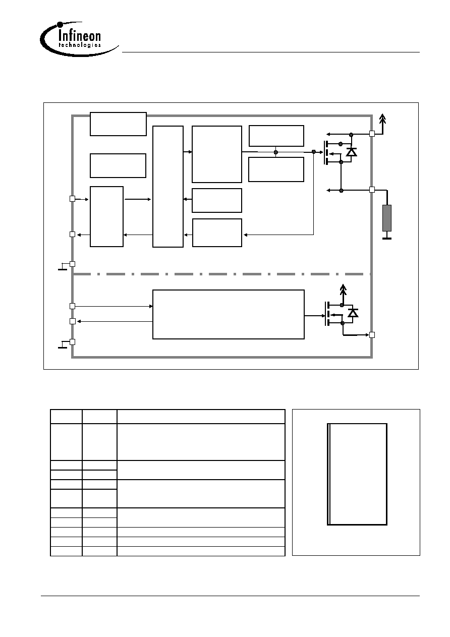
BTS 728 L2
Semiconductor Group
2
2003-Oct-01
Functional diagram
Pin Definitions and Functions
Pin
Symbol Function
1,10,
11,12,
15,16,
19,20
V
bb
Positive power supply voltage. Design the
wiring for the simultaneous max. short circuit
currents from channel 1 to 2 and also for low
thermal resistance
3 IN1
Input 1,2, activates channel 1,2 in case of
7
IN2
logic high signal
17,18 OUT1 Output 1,2, protected high-side power output
13,14
OUT2
of channel 1,2. Design the wiring for the max.
short circuit current
4 ST1
Diagnostic feedback 1,2 of channel 1,2,
8
ST2
open drain, low on failure
2 GND1
Ground 1 of chip 1 (channel 1)
6 GND2
Ground 2 of chip 2 (channel 2)
5,9 N.C. Not Connected
Pin configuration
(top view)
V
bb
1
·
20 V
bb
GND1 2
19 V
bb
IN1 3
18 OUT1
ST1 4
17 OUT1
N.C. 5
16 V
bb
GND2 6
15 V
bb
IN2 7
14 OUT2
ST2 8
13 OUT2
N.C. 9
12 V
bb
V
bb
10
11 V
bb
OUT1
GND1
overvoltage
protection
logic
internal
voltage supply
ESD
temperature
sensor
clamp for
inductive load
gate
control
+
charge
pump
current limit
Open load
detection
ST1
VBB
LOAD
IN1
PROFET
Control and protection circuit
of
channel 2
IN2
ST2
OUT2
Channel 1
GND2

BTS 728 L2
Semiconductor Group
3
2003-Oct-01
Maximum Ratings
at T
j
= 25°C unless otherwise specified
Parameter Symbol
Values
Unit
Supply voltage (overvoltage protection see page 4)
V
bb
43
V
Supply voltage for full short circuit protection
T
j,start
=
-40 ...+150°C
V
bb
24
V
Load current (Short-circuit current, see page 5)
I
L
self-limited
A
Load dump protection
1
)
V
LoadDump
= V
A
+ V
s
, V
A
= 13.5 V
R
I
2
)
= 2
, t
d
= 200
ms; IN
= low or high,
each channel loaded with R
L
=
8.0
,
V
Load
dump
3
)
60
V
Operating temperature range
Storage temperature range
T
j
T
stg
-40 ...+150
-55 ...+150
°C
Power dissipation (DC)
4)
T
a
= 25°C:
(all channels active)
T
a
= 85°C:
P
tot
3.7
1.9
W
Maximal switchable inductance, single pulse
V
bb
=
12V, T
j,start
=
150°C
4)
,
I
L
=
4.0
A, E
AS
=
220 mJ, 0
one
channel:
I
L
=
6.0
A, E
AS
=
540 mJ, 0
two parallel channels:
see diagrams on page 9
Z
L
19.9
22.3
mH
Electrostatic discharge capability (ESD)
IN:
(Human Body Model)
ST:
out to all other pins shorted:
acc. MIL-STD883D, method 3015.7 and ESD assn. std. S5.1-1993
R=1.5k
; C=100pF
V
ESD
1.0
4.0
8.0
kV
Input voltage (DC)
V
IN
-10 ... +16
V
Current through input pin (DC)
Current through status pin (DC)
see internal circuit diagram page 8
I
IN
I
ST
±
2.0
±
5.0
mA
Thermal Characteristics
Parameter and Conditions Symbol
Values
Unit
min typ
Max
Thermal resistance
junction - soldering point
4),5)
each
channel:
R
thjs
-- --
13.5
K/W
junction - ambient
4)
one channel active:
all channels active:
R
thja
--
--
41
34
--
--
1
) Supply voltages higher than V
bb(AZ)
require an external current limit for the GND and status pins (a 150
resistor for the GND connection is recommended.
2)
R
I
= internal resistance of the load dump test pulse generator
3)
V
Load dump
is setup without the DUT connected to the generator per ISO 7637-1 and DIN 40839
4
) Device on 50mm*50mm*1.5mm epoxy PCB FR4 with 6cm
2
(one layer, 70
µ
m thick) copper area for Vbb
connection. PCB is vertical without blown air. See page 14
5
) Soldering point: upper side of solder edge of device pin 15. See page 14
BTS 728 L2
Semiconductor Group
4
2003-Oct-01
Electrical Characteristics
Parameter and Conditions,
each of the two channels
Symbol
Values
Unit
at T
j
= -40...+150°C, V
bb
= 12 V unless otherwise specified
min typ
Max
Load Switching Capabilities and Characteristics
On-state resistance (Vbb to OUT);
IL = 2 A, V
bb
7V
each channel, T
j
= 25°C:
T
j
= 150°C:
two parallel channels, T
j
= 25°C:
see diagram, page 10
R
ON
--
50
100
25
60
120
30
m
Nominal load current
one channel active:
two parallel channels active:
Device on PCB
6
), Ta
=
85°C, Tj
150°C
I
L(NOM)
3.6
5.5
4.0
6.0
--
A
Output current
while GND disconnected or pulled
up
7
)
;
Vbb = 30 V, VIN = 0, see diagram page 8
I
L(GNDhigh)
-- -- 2
mA
Turn-on time
8
)
IN
to 90% V
OUT
:
Turn-off time
IN
to 10% V
OUT
:
R
L
=
12
t
on
t
off
30
30
100
100
200
200
µ
s
Slew rate on
8)
T
j
= -40°C:
10 to 30% V
OUT
,
R
L
=
12
T
j
= 25°C...150°C:
dV/dt
on
0.15
0.15
--
--
1
0.8
V/
µ
s
Slew rate off
8)
T
j
= -40°C:
70 to 40% V
OUT
, R
L
=
12
T
j
= 25°C...150°C:
-dV/dt
off
0.15
0.15
--
--
1
0.8
V/
µ
s
Operating Parameters
Operating voltage
Tj=-40
T
j
=25...150°C:
V
bb(on)
4.75 --
--
41
43
V
Overvoltage protection
9
)
T
j
=-40°C:
I
bb
=
40 mA
T
j
=25...150°C:
V
bb(AZ)
41
43
--
47
--
52
V
Standby current
10
)
T
j
=-40°C...25°C
:
V
IN
=
0;
see diagram page 10
T
j
=150°C:
I
bb(off)
--
--
10
--
18
50
µ
A
Leakage output current (included in I
bb(off)
)
V
IN
=
0
I
L(off)
-- 1
10
µ
A
Operating current
11)
, V
IN
=
5V,
I
GND
= I
GND1
+ I
GND2
,
one channel on:
two channels on:
I
GND
--
--
0.8
1.6
1.5
3.0
mA
6
) Device on 50mm*50mm*1.5mm epoxy PCB FR4 with 6cm
2
(one layer, 70
µ
m thick) copper area for Vbb
connection. PCB is vertical without blown air. See page 14
7
) not subject to production test, specified by design
8
) See timing diagram on page 11.
9)
Supply voltages higher than V
bb(AZ)
require an external current limit for the GND and status pins (a 150
resistor for the GND connection is recommended). See also V
ON(CL)
in table of protection functions and
circuit diagram on page 8.
10
) Measured with load; for the whole device; all channels off
11
)
Add I
ST
, if I
ST
> 0

BTS 728 L2
Parameter and Conditions,
each of the two channels
Symbol
Values
Unit
at T
j
= -40...+150°C, V
bb
= 12 V unless otherwise specified
min typ
Max
Semiconductor Group
5
2003-Oct-01
Protection Functions
12)
Current limit,
(see timing diagrams, page 12)
T
j
=-40°C:
T
j
=25°C:
T
j
=+150°C:
I
L(lim)
21
17
12
28
22
16
36
31
24
A
Repetitive short circuit current limit,
T
j
= T
jt
each channel
two parallel channels
(see timing diagrams, page 12)
I
L(SCr)
--
--
17
17
--
--
A
Initial short circuit shutdown time
T
j,start
=25°C:
(see timing diagrams on page 12)
t
off(SC)
--
2.4
--
ms
Output clamp (inductive load switch off)
13)
at VON(CL) = Vbb - VOUT
,
IL= 40 mA
T
j
=-40°C:
T
j
=25°C...150°C:
V
ON(CL)
41
43
--
47
--
52
V
Thermal overload trip temperature
T
jt
150 -- --
°C
Thermal hysteresis
T
jt
-- 10 --
K
Reverse Battery
Reverse battery voltage
14
)
-V
bb
--
--
32
V
Drain-source diode voltage
(V
out
> V
bb
)
I
L
=
-
4.0
A, T
j
=
+150°C
-V
ON
--
600
--
mV
12
) Integrated protection functions are designed to prevent IC destruction under fault conditions described in the
data sheet. Fault conditions are considered as "outside" normal operating range. Protection functions are not
designed for continuous repetitive operation.
13
)
If channels are connected in parallel, output clamp is usually accomplished by the channel with the lowest
V
ON(CL)
14
) Requires a 150
resistor in GND connection. The reverse load current through the intrinsic drain-source
diode has to be limited by the connected load. Power dissipation is higher compared to normal operating
conditions due to the voltage drop across the drain-source diode. The temperature protection is not active
during reverse current operation! Input and Status currents have to be limited (see max. ratings page 3 and
circuit page 8).

BTS 728 L2
Parameter and Conditions,
each of the two channels
Symbol
Values
Unit
at T
j
= -40...+150°C, V
bb
= 12 V unless otherwise specified
min typ
Max
Semiconductor Group
6
2003-Oct-01
Diagnostic Characteristics
Open load detection current,
(on-condition)
each channel
I
L (OL)
1
10
-- 500
mA
Input and Status Feedback
15
)
Input resistance
(see circuit page 8)
R
I
2.5
3.5 6
k
Input turn-on threshold voltage
V
IN(T+)
1.7 --
3.2
V
Input turn-off threshold voltage
V
IN(T-)
1.5 -- --
V
Input threshold hysteresis
V
IN(T)
-- 0.5 --
V
Off state input current
V
IN
= 0.4 V: I
IN(off)
1
-- 50
µ
A
On state input current
V
IN
= 5 V: I
IN(on)
20 50 90
µ
A
Delay time for status with open load after switch
off; (
see diagram on page 13)
t
d(ST OL4)
100 520 900
µ
s
Status invalid after positive input slope
(open load)
t
d(ST)
-- --
500
µ
s
Status output (open drain)
Zener limit voltage
I
ST
= +1.6 mA:
ST low voltage
I
ST
= +1.6 mA:
V
ST(high)
V
ST(low)
5.4
--
6.1
--
--
0.4
V
15)
If ground resistors R
GND
are used, add the voltage drop across these resistors.

BTS 728 L2
Semiconductor Group
7
2003-Oct-01
Truth Table
Channel 1
Input 1 Output 1
Status 1
Channel 2
Input 2 Output 2
Status 2
level
level
BTS 728L2
Normal
operation
L
H
L
H
H
H
Open load
L
H
Z
H
H
L
Overtem-
perature
L
H
L
L
H
L
L = "Low" Level
X = don't care
Z = high impedance, potential depends on external circuit
H = "High" Level
Status signal valid after the time delay shown in the timing diagrams
Parallel switching of channel 1 and 2 is easily possible by connecting the inputs and outputs in parallel. The
status outputs ST1 and ST2 have to be configured as a 'Wired OR' function with a single pull-up resistor.
Terms
PROFET
IN1
ST1
OUT1
GND1
Vbb
VST1
V IN1
I IN1
V
bb
I L1
VOUT1
IGND1
VON1
2
3
4
Leadframe
17,18
Ibb
I ST1
R GND1
Chip 1
PROFET
IN2
ST2
OUT2
GND2
Vbb
VST2
V
IN2
I IN2
I L2
VOUT2
IGND2
VON2
6
7
8
Leadframe
13,14
I ST2
R GND2
Chip 2
Leadframe (V
bb
) is connected to pin 1,10,11,12,15,16,19,20
External R
GND
optional; two resistors R
GND1
, R
GND2
=
150
or a single resistor R
GND
=
75
for reverse
battery protection up to the max. operating voltage.

BTS 728 L2
Semiconductor Group
8
2003-Oct-01
Input circuit (ESD protection),
IN1 or IN2
IN
GND
I
R
ESD-ZD
I
I
I
The use of ESD zener diodes as voltage clamp at DC
conditions is not recommended.
Status output,
ST1 or ST2
ST
GND
ESD-
ZD
+5V
R
ST(ON)
ESD-Zener diode: 6.1
V typ., max 5.0 mA; R
ST(ON)
< 375
at 1.6 mA. The use of ESD zener diodes as voltage clamp at
DC conditions is not recommended.
Inductive and overvoltage output clamp,
OUT1 or OUT2
+Vbb
OUT
VZ
V
ON
Power GND
V
ON
clamped to V
ON(CL)
= 47 V typ.
Overvolt. and reverse batt. protection
+ Vbb
IN
ST
ST
R
GND
GND
R
Signal GND
Logic
PROFET
VZ2
I
R
VZ1
Load GND
Load
R
OUT
ST
R
+ 5V
V
Z1
= 6.1 V typ., V
Z2
= 47 V typ., R
GND
= 150
,
R
ST
= 15 k
, R
I
= 3.5 k
typ.
In case of reverse battery the load current has to be
limited by the load. Temperature protection is not
active
Open-load detection
OUT1 or OUT2
ON-state diagnostic
Open load, if V
ON
< R
ON
·
I
L(OL)
; IN high
Open load
detection
Logic
unit
+ Vbb
OUT
ON
V
ON
GND disconnect
PROFET
V
IN
ST
OUT
GND
bb
V
bb
V
IN
V
ST
V
GND
Any kind of load. In case of IN
=
high is V
OUT
V
IN
-
V
IN(T+)
.
Due to V
GND
>
0, no V
ST
= low signal available.
BTS 728 L2
Semiconductor Group
9
2003-Oct-01
GND disconnect with GND pull up
PROFET
V
IN
ST
OUT
GND
bb
V
bb
V
GND
V
IN
V
ST
Any kind of load. If V
GND
> V
IN
- V
IN(T+)
device stays off
Due to V
GND
>
0, no V
ST
= low signal available.
V
bb
disconnect with energized inductive
load
PROFET
V
IN
ST
OUT
GND
bb
V
bb
high
For inductive load currents up to the limits defined by Z
L
(max. ratings and diagram on page 9) each switch is
protected against loss of Vbb.
Consider at your PCB layout that in the case of Vbb dis-
connection with energized inductive load all the load current
flows through the GND connection.
Inductive load switch-off energy
dissipation
PROFET
V
IN
ST
OUT
GND
bb
=
E
E
E
EAS
bb
L
R
ELoad
RL
L
{
L
Z
Energy stored in load inductance:
E
L
=
1/2
·
L
·
I
2
L
While demagnetizing load inductance, the energy
dissipated in PROFET is
E
AS
= E
bb
+ E
L
- E
R
=
V
ON(CL)
·
i
L
(t) dt,
with an approximate solution for RL
>
0
:
E
AS
=
I
L
·
L
2
·
R
L
(
V
bb
+
|V
OUT(CL)
|)
ln
(1+
I
L
·
R
L
|V
OUT(CL)
|
)
Maximum allowable load inductance for
a single switch off
(one channel)
4)
L = f (IL );
Tj,start =
150°C, Vbb =
12
V, RL =
0
ZL [mH]
1
10
100
1000
2
3
4
5
6
7
8
9
10 11 12
IL [A]
BTS 728 L2
Semiconductor Group
10
2003-Oct-01
Typ. on-state resistance
R
ON
= f (Vbb,Tj )
; I
L
=
2
A, IN
= high
R
ON
[mOhm]
125
100
75
50
25
0
3 5 7 9
30
40
Tj = 150°C
25°C
-40°C
V
bb
[V]
Typ. standby current
I
bb(off)
= f (T
j
)
; V
bb
= 9...34 V, IN1,2
= low
I
bb(off)
[
µ
A]
0
5
10
15
20
25
30
35
40
45
-50
0
50
100
150
200
T
j
[°C]

BTS 728 L2
Semiconductor Group
11
2003-Oct-01
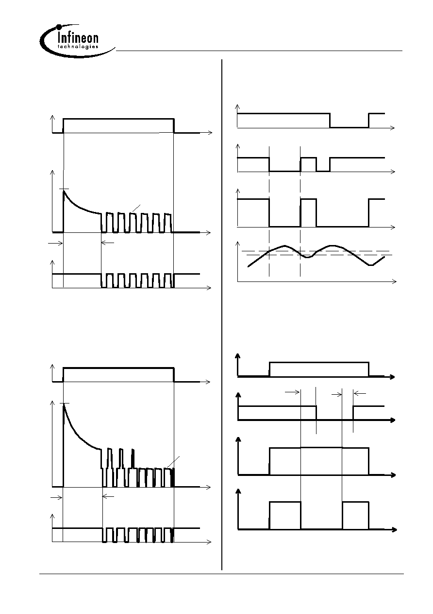
Figure 1a: V
bb
turn on:
IN2
V
OUT1
t
V
bb
ST1 open drain
IN1
V
OUT2
ST2 open drain
Figure 2a: Switching a resistive load,
turn-on/off time and slew rate definition:
IN
t
V
OUT
I
L
t
t
on
off
90%
dV/dton
dV/dtoff
10%
Figure 2b: Switching a lamp:
IN
ST
OUT
L
t
V
I
The initial peak current should be limited by the lamp and not by the
current limit of the device.
Figure 2c: Switching an inductive load
IN
ST
L
t
V
I
OUT
I
L(OL)
Timing diagrams
Both channels are symmetric and consequently the diagrams are valid for channel 1 and
channel 2
BTS 728 L2
Semiconductor Group
12
2003-Oct-01
*) if the time constant of load is too large, open-load-status may
occur
Figure 3a: Turn on into short circuit:
shut down by overtemperature, restart by cooling
other channel: normal operation
t
I
ST
IN1
L1
L(SCr)
I
I
L(lim)
toff(SC)
Heating up of the chip may require several milliseconds, depending
on external conditions
Figure 3b: Turn on into short circuit:
shut down by overtemperature, restart by cooling
(two parallel switched channels 1 and 2)
t
ST1/2
IN1/2
L1 L2
L(SCr)
I
2xIL(lim)
I + I
toff(SC)
ST1 and ST2 have to be configured as a 'Wired OR' function
ST1/2 with a single pull-up resistor.
Figure 4a: Overtemperature:
Reset if T
j
<T
jt
IN
ST
OUT
J
t
V
T
Figure 5a: Open load: detection in ON-state, open
load occurs in on-state
IN
ST
OUT
L
t
V
I
open
normal
normal
t
d(ST OL)
t
d(ST OL)
t
d(ST OL)
= 10
µ
s typ.
BTS 728 L2
Semiconductor Group
13
2003-Oct-01
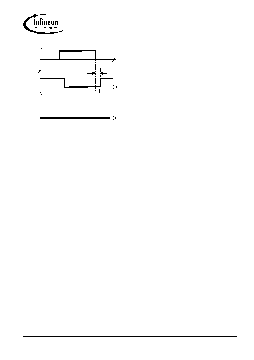
Figure 5b: Open load: turn on/off to open load
IN
ST
L
t
I
t
d(STOL4)
BTS 728 L2
Semiconductor Group
14
2003-Oct-01
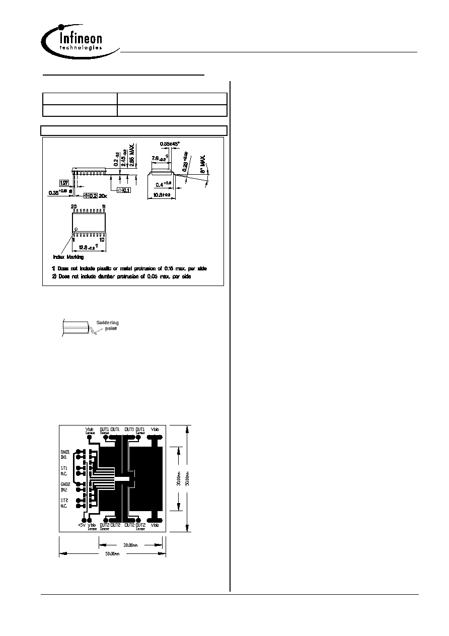
Package and Ordering Code
Standard: P-DSO-20-9
Sales Code
BTS 728 L2
Ordering
Code Q67060-S7014-A2
All dimensions in millimetres
Definition of soldering point with temperature T
s
:
upper side of solder edge of device pin 15.
Pin 15
Printed circuit board (FR4, 1.5mm thick, one layer
70
µ
m, 6cm
2
active heatsink area) as a reference for
max. power dissipation P
tot
, nominal load current
I
L(NOM)
and thermal resistance R
thja
Published by
Infineon Technologies AG,
St.-Martin-Strasse 53,
D-81669 München
© Infineon Technologies AG 2001
All Rights Reserved.
Attention please!
The information herein is given to describe certain components and
shall not be considered as a guarantee of characteristics.
Terms of delivery and rights to technical change reserved.
We hereby disclaim any and all warranties, including but not limited
to warranties of non-infringement, regarding circuits, descriptions
and charts stated herein.
Infineon Technologies is an approved CECC manufacturer.
Information
For further information on technology, delivery terms and conditions
and prices please contact your nearest Infineon Technologies Office
in Germany or our Infineon Technologies Representatives worldwide
(see address list).
Warnings
Due to technical requirements components may contain dangerous
substances. For information on the types in question please contact
your nearest Infineon Technologies Office.
Infineon Technologies Components may only be used in life-support
devices or systems with the express written approval of Infineon
Technologies, if a failure of such components can reasonably be
expected to cause the failure of that life-support device or system, or
to affect the safety or effectiveness of that device or system. Life
support devices or systems are intended to be implanted in the
human body, or to support and/or maintain and sustain and/or
protect human life. If they fail, it is reasonable to assume that the
health of the user or other persons may be endangered.