
D a t a S h e e t , V 1 . 0 , J a n u a r y 2 0 0 4
N e v e r s t o p t h i n k i n g .
B T S 5 2 3 4 G
S m a r t H i g h - S i d e P o w e r S w i t c h
P R O F E T
T w o C h a n n e l s , 6 0 m
A u t o m o t i v e P o w e r

Smart High-Side Power Switch
BTS 5234G
Table of Contents
Page
Data Sheet
2
V1.0, 2004-01-23
Product Summary . . . . . . . . . . . . . . . . . . . . . . . . . . . . . . . . . . . . . . . . . . . . . . . . . . . .3
1 Overview . . . . . . . . . . . . . . . . . . . . . . . . . . . . . . . . . . . . . . . . . . . . . . . . . . . . . . . . .5
1.1 Block Diagram . . . . . . . . . . . . . . . . . . . . . . . . . . . . . . . . . . . . . . . . . . . . . . . . . . .5
1.2 Terms . . . . . . . . . . . . . . . . . . . . . . . . . . . . . . . . . . . . . . . . . . . . . . . . . . . . . . . . .6
2 Pin Configuration . . . . . . . . . . . . . . . . . . . . . . . . . . . . . . . . . . . . . . . . . . . . . . . . . .7
2.1 Pin Assignment BTS 5234G . . . . . . . . . . . . . . . . . . . . . . . . . . . . . . . . . . . . . . . .7
2.2 Pin Definitions and Functions . . . . . . . . . . . . . . . . . . . . . . . . . . . . . . . . . . . . . . .7
3 Electrical Characteristics . . . . . . . . . . . . . . . . . . . . . . . . . . . . . . . . . . . . . . . . . . . .8
3.1 Maximum Ratings . . . . . . . . . . . . . . . . . . . . . . . . . . . . . . . . . . . . . . . . . . . . . . . .8
4 Block Description and Electrical Characteristics . . . . . . . . . . . . . . . . . . . . . . .10
4.1 Power Stages . . . . . . . . . . . . . . . . . . . . . . . . . . . . . . . . . . . . . . . . . . . . . . . . . .10
4.1.1
Output On-State Resistance . . . . . . . . . . . . . . . . . . . . . . . . . . . . . . . . . . 10
4.1.2
Input Circuit . . . . . . . . . . . . . . . . . . . . . . . . . . . . . . . . . . . . . . . . . . . . . . . 10
4.1.3
Inductive Output Clamp . . . . . . . . . . . . . . . . . . . . . . . . . . . . . . . . . . . . . . 11
4.1.4
Electrical Characteristics . . . . . . . . . . . . . . . . . . . . . . . . . . . . . . . . . . . . 13
4.2 Protection Functions . . . . . . . . . . . . . . . . . . . . . . . . . . . . . . . . . . . . . . . . . . . . .15
4.2.1
Over Load Protection . . . . . . . . . . . . . . . . . . . . . . . . . . . . . . . . . . . . . . . . 15
4.2.2
Reverse Polarity Protection . . . . . . . . . . . . . . . . . . . . . . . . . . . . . . . . . . . 16
4.2.3
Over Voltage Protection . . . . . . . . . . . . . . . . . . . . . . . . . . . . . . . . . . . . . 16
4.2.4
Loss of Ground Protection . . . . . . . . . . . . . . . . . . . . . . . . . . . . . . . . . . . . 16
4.2.5
Electrical Characteristics . . . . . . . . . . . . . . . . . . . . . . . . . . . . . . . . . . . . 17
4.3 Diagnosis . . . . . . . . . . . . . . . . . . . . . . . . . . . . . . . . . . . . . . . . . . . . . . . . . . . . . .18
4.3.1
ON-State Diagnosis . . . . . . . . . . . . . . . . . . . . . . . . . . . . . . . . . . . . . . . . . 19
4.3.2
OFF-State Diagnosis . . . . . . . . . . . . . . . . . . . . . . . . . . . . . . . . . . . . . . . . 20
4.3.3
Sense Enable Function . . . . . . . . . . . . . . . . . . . . . . . . . . . . . . . . . . . . . . 21
4.3.4
Electrical Characteristics . . . . . . . . . . . . . . . . . . . . . . . . . . . . . . . . . . . . 22
5 Package Outlines BTS 5234G . . . . . . . . . . . . . . . . . . . . . . . . . . . . . . . . . . . . . . .24
6 Revision History . . . . . . . . . . . . . . . . . . . . . . . . . . . . . . . . . . . . . . . . . . . . . . . . . .25
Data Sheet
3
V1.0, 2004-01-23
Type
Ordering Code
Package
BTS 5234G
Q67060-S6156
P-DSO-20-21
Smart High-Side Power Switch
PROFET
BTS 5234G
Product Summary
The BTS 5234G is a dual channel high-side power
switch in P-DSO-20-21 package providing embedded
protective functions.
The power transistor is built by a N-channel vertical
power MOSFET with charge pump. The device is
monolithically integrated in Smart SIPMOS
technology.
Basic Features
· Very low standby current
· 3.3 V and 5 V compatible logic pins
· Improved electromagnetic compatibility (EMC)
· Stable behavior at under voltage
· Logic ground independent from load ground
· Secure load turn-off while logic ground disconnected
· Optimized inverse current capability
Operating voltage
V
bb(on)
4.5 .. 28 V
Over voltage protection
V
bb(AZ)
41 V
On-State resistance
R
DS(ON)
60 m
Nominal load current (one channel active)
I
L(nom)
3.3 A
Current limitation
I
L(LIM)
23 A
Current limitation repetitive
I
L(SCr)
6 A
Standby current for whole device with load
I
bb(OFF)
2.5 µA
P-DSO-20-21

Smart High-Side Power Switch
BTS 5234G
Data Sheet
4
V1.0, 2004-01-23
Protective Functions
· Reverse battery protection without external components
· Short circuit protection
· Overload protection
· Multi-step current limitation
· Thermal shutdown with restart
· Thermal restart at reduced current limitation
· Over voltage protection without external resistor
· Loss of ground protection
· Electrostatic discharge protection (ESD)
Diagnostic Functions
· Enhanced IntelliSense signal for each channel
· Enable function for diagnosis pins (IS1 and IS2)
· Proportional load current sense signal by current source
· High accuracy of current sense signal at wide load current range
· Open load detection in ON-state by load current sense
· Open load detection in OFF-state by voltage source
· Feedback on over temperature and current limitation in ON-state
Applications
· µC compatible high-side power switch with diagnostic feedback for 12 V grounded
loads
· All types of resistive, inductive and capacitive loads
· Suitable for loads with high inrush currents, so as lamps
· Suitable for loads with low currents, so as LEDs
· Replaces electromechanical relays, fuses and discrete circuits
Smart High-Side Power Switch
BTS 5234G
Overview
Data Sheet
5
V1.0, 2004-01-23
1
Overview
The BTS 5234G is a dual channel high-side power switch (two times 60 m
) in
P-DSO-20-21 package providing embedded protective functions.
The Enhanced IntelliSense pins IS1 and IS2 provide a sophisticated diagnostic feedback
signal including current sense function and open load in off state. The diagnosis signals
can be switched on and off by the sense enable pin SEN.
An integrated ground resistor as well as integrated resistors at each input pin (IN1, IN2,
SEN) reduce external components to a minimum.
The power transistor is built by a N-channel vertical power MOSFET with charge pump.
The inputs are ground referenced CMOS compatible. The device is monolithically
integrated in Smart SIPMOS technology.
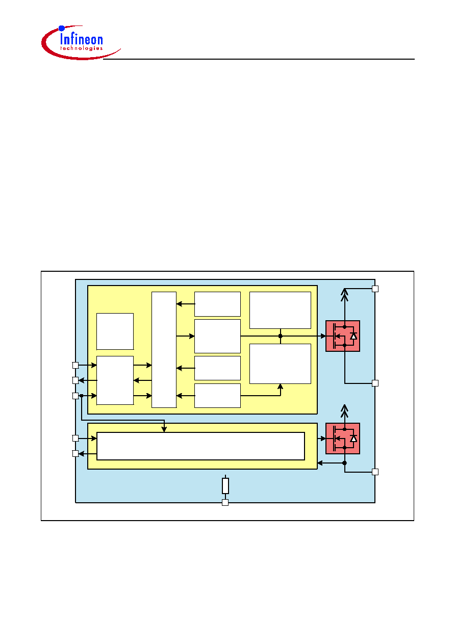
1.1
Block Diagram
Figure 1
Block Diagram
channel 1
internal
power
supply
ESD
protection
OUT2
channel 2
control and protection circuit
equivalent to
channel 1
IN1
IS1
SEN
GND
R
GND
IS2
IN2
open load
detection
logic
gate control
&
charge pump
VBB
OUT1
clamp for
inductive load
multi step
load current
limitation
load current
sense
temperature
sensor