2004-01-27
Page 1
BTS 452 T
Smart Power High-Side-Switch
Features
À
Overload protection
À
Current limitation
À
Short circuit protection
À
Thermal shutdown with restart
À
Overvoltage protection
(including load dump)
À
Fast demagnetization of inductive loads
À
Reverse battery protection
with external resistor
À
CMOS compatible input
À
Loss of GND and loss of V
bb
protection
À
ESD - Protection
À
Very low standby current
Product Summary
Overvoltage protection
V
bb(AZ)
62
V
Operating voltage
V
bb(on)
6...52 V
On-state resistance
R
ON
200
m
Nominal load current
I
L(ISO)
1.8
A
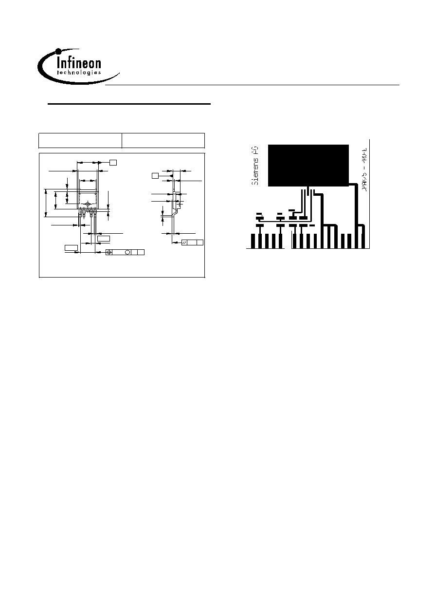
P-TO252-5-11
Application
À
All types of resistive, inductive and capacitive loads
À
ÁC compatible power switch for 12 V, 24 V and 42 V DC applications
À
Replaces electromechanical relays and discrete circuits
General Description
N channel vertical power FET with charge pump, ground referenced CMOS compatible input,
monolithically integrated in Smart SIPMOS
technology.
Providing embedded protective functions.

2004-01-27
Page 2
BTS 452 T
Block Diagram
+ Vbb
IN
Signal GND
ESD
miniPROFET
OUT
GND
Logic
Voltage
source
Charge pump
Level shifter
Temperature
sensor
Rectifier
Limit for
unclamped
ind. loads
Gate
protection
Current
limit
Load GND
Load
V
Logic
Overvoltage
protection
Pin
Symbol
Function
1
GND
Logic ground
2
IN
Input, activates the power switch in case of logic high signal
3
Vbb
Positive power supply voltage
4
NC
not connected
5
OUT
Output to the load
TAB
Vbb
Positive power supply voltage
Pin configuration
Tab = V
BB
1 2 (3) 4 5
GND IN NC OUT
Top view

2004-01-27
Page 3
BTS 452 T
Maximum Ratings at T
j
= 25░C, unless otherwise specified
Parameter
Symbol
Value
Unit
Supply voltage
V
bb
52
V
Supply voltage for full short circuit protection
V
bb(SC)
50
Continuous input voltage
V
IN
-10 ... +16
Load current (Short - circuit current, see page 5) I
L
self limited
A
Current through input pin (DC)
I
IN
▒
5
mA
Operating temperature
T
j
-40 ...+150
░C
Storage temperature
T
stg
-55 ... +150
Power dissipation
1)
P
tot
41.6
W
Inductive load switch-off energy dissipation
1)2)
single pulse, (see page 8)
Tj =150 ░C, I
L
= 1 A
E
AS
150
mJ
Load dump protection
2)
V
LoadDump
3)
= V
A
+ V
S
R
I
=2
, t
d
=400ms, V
IN
= low or high, V
A
=13,5V
R
L
= 13.5
R
L
= 27
V
Loaddump
73.5
88.5
V
Electrostatic discharge voltage
(Human Body Model)
according to ANSI EOS/ESD - S5.1 - 1993
ESD STM5.1 - 1998
Input pin
all other pins
V
ESD
▒
1
▒
5
kV
Thermal Characteristics
junction - case:
R
thJC
-
-
3
K/W
Thermal resistance @ min. footprint
R
th(JA)
-
80
-
K/W
Thermal resistance @ 6 cm
2
cooling area
1)
R
th(JA)
-
45
60
1Device on 50mm*50mm*1.5mm epoxy PCB FR4 with 6 cm2 (one layer, 70Ám thick) copper area for drain
connection. PCB is vertical without blown air. (see page 16)
2not subject to production test, specified by design
3VLoaddump is setup without the DUT connected to the generator per ISO 7637-1 and DIN 40839 .
Supply voltages higher than Vbb(AZ) require an external current limit for the GND pin, e.g. with a
150
resistor in GND connection. A resistor for the protection of the input is integrated.

2004-01-27
Page 4
BTS 452 T
Electrical Characteristics
Parameter and Conditions
Symbol
Values
Unit
at T
j
= -40...150░C, V
bb
= 12..42V,
unless otherwise specified
min.
typ.
max.
Load Switching Capabilities and Characteristics
On-state resistance
T
j
= 25 ░C, I
L
= 1 A, V
bb
= 9...52 V
T
j
= 150 ░C
R
ON
-
-
150
270
200
380
m
Nominal load current; Device on PCB
1)
T
C
= 85 ░C, V
ON
= 0.5 V
I
L(ISO)
1.8
2.2
-
A
Turn-on time to 90%
V
OUT
R
L
= 47
t
on
-
80
180
Ás
Turn-off time to 10%
V
OUT
R
L
= 47
t
off
-
80
200
Slew rate on 10 to 30% V
OUT
,
R
L
= 47
, V
bb
= 13.5 V
dV/dt
on
-
0.7
2
V/Ás
Slew rate off 70 to 40% V
OUT
,
R
L
= 47
, V
bb
= 13.5 V
-dV/dt
off
-
0.9
2
Operating Parameters
Operating voltage
V
bb(on)
6
-
52
V
Undervoltage shutdown of charge pump
T
j
= -40...+85 ░C
T
j
= 150 ░C
V
bb(under)
-
-
-
-
4
5.5
Undervoltage restart of charge pump
V
bb(u cp)
-
4
5.5
Standby current
T
j
= -40...+85 ░C, V
IN
= low
T
j
= +150 ░C
2)
, V
IN
= low
I
bb(off)
-
-
-
-
15
18
ÁA
Leakage output current (included in
I
bb(off)
)
V
IN
= low
I
L(off)
-
-
5
Operating current
V
IN
= high
I
GND
-
0.8
2
mA
1Device on 50mm*50mm*1.5mm epoxy PCB FR4 with 6 cm2 (one layer, 70Ám thick) copper area for drain
connection. PCB is vertical without blown air. (see page 16)
2higher current due temperature sensor

2004-01-27
Page 5
BTS 452 T
Electrical Characteristics
Parameter and Conditions
Symbol
Values
Unit
at T
j
= -40...150░C, V
bb
= 12..42V,
unless otherwise specified
min.
typ.
max.
Protection Functions
1)
Initial peak short circuit current limit (pin 3 to 5)
T
j
= -40 ░C, V
bb
= 20 V, t
m
= 150 Ás
T
j
= 25 ░C
T
j
= 150 ░C
T
j
= -40...+150 ░C, V
bb
> 40 V , ( see page 11 )
I
L(SCp)
-
-
4
-
-
6.5
-
5
2)
9
-
-
-
A
Repetitive short circuit current limit
T
j
= T
jt
(see timing diagrams)
V
bb
< 40 V
V
bb
> 40 V
I
L(SCr)
-
-
6
4.5
-
-
Output clamp (inductive load switch off)
at V
OUT
= V
bb
- V
ON(CL)
,
I
bb
= 4 mA
V
ON(CL)
59
63
-
V
Overvoltage protection
3)
I
bb
= 4 mA
V
bb(AZ)
62
-
-
Thermal overload trip temperature
T
jt
150
-
-
░C
Thermal hysteresis
T
jt
-
10
-
K
Reverse Battery
Reverse battery
4)
-V
bb
-
-
52
V
Drain-source diode voltage (V
OUT
> V
bb
)
T
j
= 150 ░C
-V
ON
-
600
-
mV
1Integrated protection functions are designed to prevent IC destruction under fault conditions
described in the data sheet. Fault conditions are considered as "outside" normal operating range.
Protection functions are not designed for continuous repetitive operation .
2not subject to production test, specified by design
3 see also VON(CL) in circuit diagram on page 7
4Requires a 150
resistor in GND connection. The reverse load current through the intrinsic drain-source diode has
to be limited by the connected load. Power dissipation is higher compared to normal operating conditions due to the
voltage drop across the drain-source diode. The temperature protection is not active during reverse current operation!
Input current has to be limited (see max. ratings page 3).

2004-01-27
Page 6
BTS 452 T
Parameter and Conditions
Symbol
Values
Unit
at T
j
= -40...150░C, V
bb
= 12..42V,
unless otherwise specified
min.
typ.
max.
Input
Input turn-on threshold voltage
V
IN(T+)
-
-
2.2
V
Input turn-off threshold voltage
V
IN(T-)
0.8
-
-
Input threshold hysteresis
V
IN(T)
-
0.4
-
Off state input current
V
IN
= 0.7 V
I
IN(off)
1
-
25
ÁA
On state input current
V
IN
= 5 V
I
IN(on)
3
-
25
Input resistance (see page 7)
R
I
2
3.5
5
k

2004-01-27
Page 7
BTS 452 T
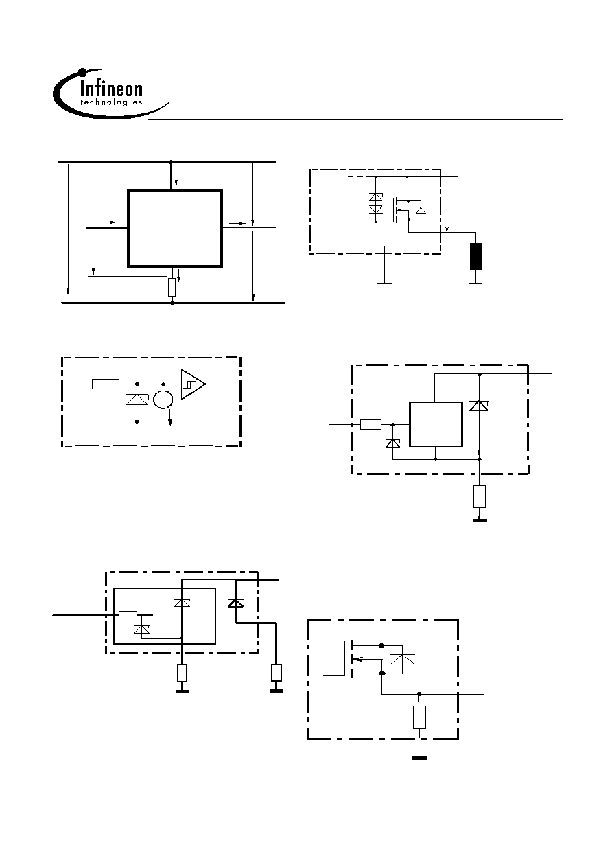
Terms
Inductive and overvoltage output clamp
+ Vbb
OUT
GND
VZ
VON
PROFET
V
IN
OUT
GND
bb
V IN
IIN
V
bb
Ibb
IL
VOUT
IGND
VON
RGND
VON clamped to 59V min.
Overvoltage protection of logic part
Input circuit (ESD protection)
+ Vbb
IN
GND
GND
R
Signal GND
Logic
V
Z2
I
R
V
Z1
IN
GND
I
R
ZD
I
I
I
ESD-
The use of ESD zener diodes as voltage clamp
at DC conditions is not recommended
V
Z1
=6.1V typ., V
Z2
=V
bb(AZ)
=62V min.,
R
I
=3.5 k
typ., R
GND
=150
Reverse battery protection
Internal output pull down
GND
Logic
IN
OUT
L
R
Power GND
GND
R
Signal GND
Power
Inverse
I
R
Vbb
-
Diode
V OUT
Signal G ND
R O
V
bb
R
GND
=150
, R
I
=3.5k
typ.,
Temperature protection is not active during
inverse current
R
O
= 200 k
typ.

2004-01-27
Page 8
BTS 452 T
Vbb disconnect with charged inductive
load
PROFET
V
IN
OUT
GND
bb
V
bb
high
GND disconnect
PROFET
V
IN
OUT
GND
bb
V
bb
V
IN
V
GND
Inductive Load switch-off energy
dissipation
PROFET
V
IN
OUT
GND
bb
=
E
E
E
EAS
bb
L
R
ELoad
RL
L
{
L
Z
GND disconnect with GND pull up
PROFET
V
IN
OUT
GND
bb
V
bb
V
GND
V
IN
Energy stored in load inductance: E
L
= ¢ * L * I
L
2
While demagnetizing load inductance,
the enÚrgy dissipated in PROFET is
E
AS
= E
bb
+ E
L
- E
R
=
V
ON(CL)
* i
L
(t) dt,
with an approximate solution for R
L
> 0
:
E
I
L
R
V
V
I
R
V
A S
L
L
b b
O U T C L
L
L
O U T C L
=
+
+
*
*
* (
|
) * ln (
*
|
|
)
(
)|
(
)
2
1

2004-01-27
Page 9
BTS 452 T
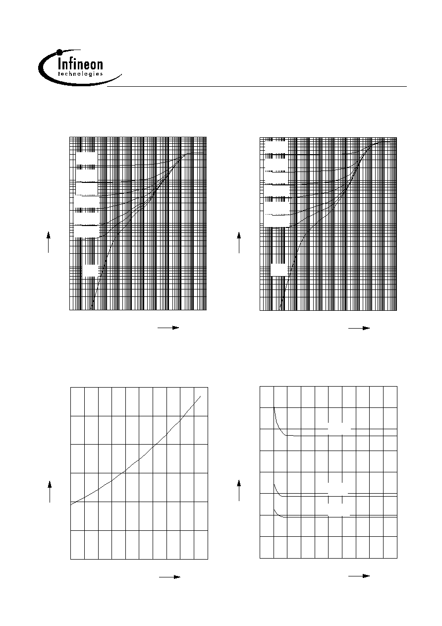
Typ. transient thermal impedance
Z
thJA
=f(t
p
) @ 6cm
2
heatsink area
Parameter: D=t
p
/T
10
-7
10
-6
10
-5
10
-4
10
-3
10
-2
10
-1
10
0
10
1
10
2
10
4
s
t
p
-2
10
-1
10
0
10
1
10
2
10
K/W
Z
thJA
D=0
D=0.01
D=0.02
D=0.05
D=0.1
D=0.2
D=0.5
Typ. transient thermal impedance
Z
thJA
=f(t
p
) @ min. footprint
Parameter: D=t
p
/T
10
-7
10
-6
10
-5
10
-4
10
-3
10
-2
10
-1
10
0
10
1
10
2
10
4
s
t
p
-2
10
-1
10
0
10
1
10
2
10
K/W
Z
thJA
D=0
D=0.01
D=0.02
D=0.05
D=0.1
D=0.2
D=0.5
Typ. on-state resistance
R
ON
= f(V
bb
); I
L
= 1 A ; V
in
= high
0
5
10
15
20
25
30
35
40
V
50
V
bb
0
50
100
150
200
250
300
m
400
R
ON
-40░C
25░C
150░C
Typ. on-state resistance
R
ON
= f(T
j
) ; V
bb
= 13,5V ; V
in
= high
-40 -20
0
20
40
60
80 100 120
░C
160
T
j
0
50
100
150
200
m
300
R
ON

2004-01-27
Page 10
BTS 452 T
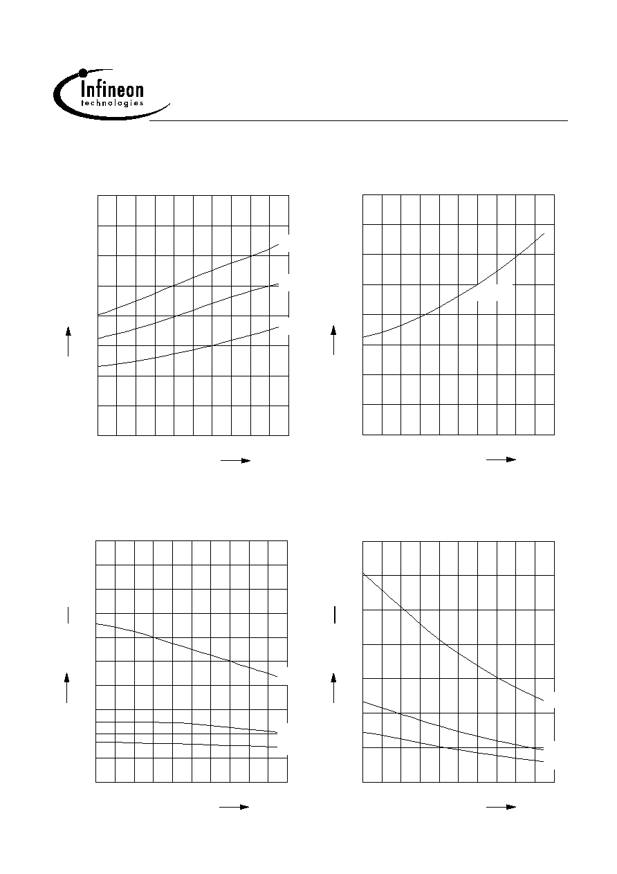
Typ. turn off time
t
off
= f(T
j
); R
L
= 47
-40 -20
0
20
40
60
80 100 120
░C
160
T
j
0
20
40
60
80
100
120
Ás
160
t
off
9...42V
Typ. turn on time
t
on
= f(T
j
); R
L
= 47
-40 -20
0
20
40
60
80 100 120
░C
160
T
j
0
20
40
60
80
100
120
Ás
160
t
on
9V
13.5V
42V
Typ. slew rate on
dV/dt
on
= f(T
j
) ; R
L
= 47
-40 -20
0
20
40
60
80 100 120
░C
160
T
j
0
0.2
0.4
0.6
0.8
1
1.2
1.4
1.6
V/Ás
2
d
V
d
t
on
9V
13.5V
42V
Typ. slew rate off
dV/dt
off
= f(T
j
); R
L
= 47
-40 -20
0
20
40
60
80 100 120
░C
160
T
j
0
0.5
1
1.5
2
2.5
V/Ás
3.5
-d
V
d
t
off
9V
13.5V
42V

2004-01-27
Page 11
BTS 452 T
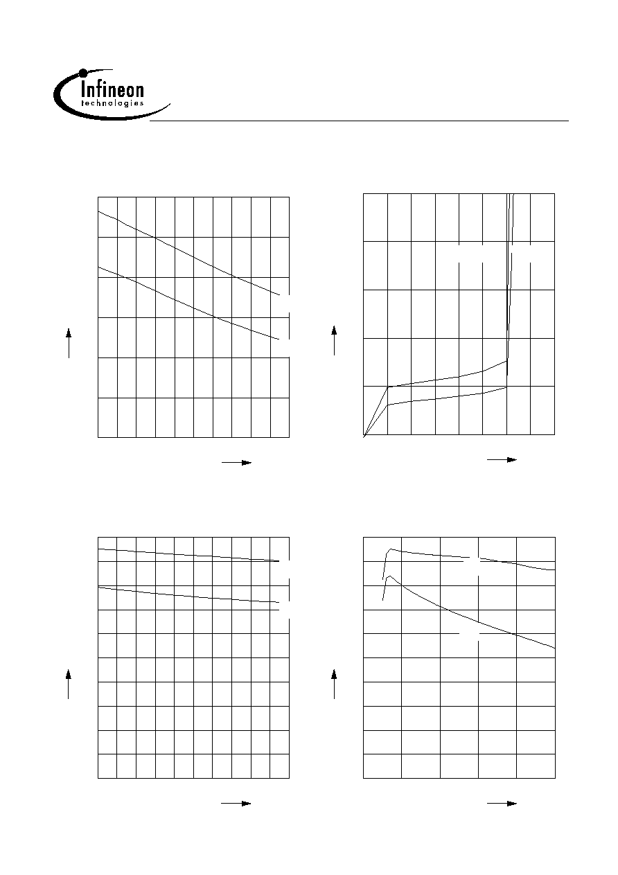
Typ. leakage current
I
L(off)
= f(T
j
) ; V
bb
= 42V ; V
IN
= low
-40 -20
0
20
40
60
80 100 120
░C
160
T
j
0
0.5
1
1.5
ÁA
2.5
I
L(off)
Typ. standby current
I
bb(off)
= f(T
j
) ; V
bb
= 42V ; V
IN
= low
-40 -20
0
20
40
60
80 100 120
░C
160
T
j
0
2
4
6
ÁA
10
I
bb(off)
Typ. initial peak short circuit current limit
I
L(SCp)
= f(V
bb
)
0
10
20
30
40
V
60
V
bb
0
2
4
6
A
10
I
L(SCp)
-40░C
25░C
150░C
Typ. initial short circuit shutdown time
t
off(SC)
= f(T
j,start
) ; V
bb
= 20V
-40 -20
0
20
40
60
80 100 120
░C
160
T
j
0
1
2
3
4
ms
6
t
off(SC)

2004-01-27
Page 12
BTS 452 T
Typ. input current
I
IN
= f(V
IN
); V
bb
= 13.5V
0
1
2
3
4
5
6
V
8
V
IN
0
10
20
30
ÁA
50
I
IN
-40...25░C
150░C
Typ. input current
I
IN(on/off)
= f(T
j
); V
bb
= 13,5V; V
IN
= low/high
V
IN
low
0,7V;
V
IN
high
= 5V
-40 -20
0
20
40
60
80 100 120
░C
160
T
j
0
2
4
6
8
ÁA
12
I
IN
on
off
Typ. input threshold voltage
V
IN(th)
= f(T
j
) ; V
bb
= 13,5V
-40 -20
0
20
40
60
80 100 120
░C
160
T
j
0
0.2
0.4
0.6
0.8
1
1.2
1.4
1.6
V
2
V
IN(th)
on
off
Typ. input threshold voltage
V
IN(th)
= f(V
bb
) ; T
j
= 25░C
0
10
20
30
V
50
V
bb
0
0.2
0.4
0.6
0.8
1
1.2
1.4
1.6
V
2
V
IN(th)
on
off

2004-01-27
Page 13
BTS 452 T
Maximum allowable load inductance
for a single switch off
L = f(I
L
); T
jstart
=150░C, R
L
=0
0
0.25
0.5
0.75
1
1.25
1.5
A
2
I
L
0
500
1000
1500
2000
2500
3000
3500
mH
4500
L
13.5V
42V
Maximum allowable inductive switch-off
energy, single pulse
E
AS
= f(I
L
); T
jstart
= 150░C, V
bb
= 13,5V
0
0.25
0.5
0.75
1
1.25
1.5
A
2
I
L
0
200
400
600
800
mJ
1200
E
AS

2004-01-27
Page 14
BTS 452 T
Timing diagrams
Figure 2b: Switching a lamp,
Figure 1a: Vbb turn on:
IN
OUT
L
t
I
IN
V
OUT
V
bb
t
Figure 2a: Switching a resistive load,
turn-on/off time and slew rate definition
Figure 2c: Switching an inductive load
IN
t
V
O U T
I
L
t
t
o n
o f f
9 0 %
d V /d t o n
d V /d to f f
1 0 %
IN
L
t
V
I
OUT

2004-01-27
Page 15
BTS 452 T
Figure 3a: Turn on into short circuit,
shut down by overtemperature, restart by cooling
t
I
IN
L
L(SCr)
I
I
L(SCp)
t
off(SC)
t
m
t
Figure 5: Undervoltage restart of charge pump
Heating up of the chip may require several milliseconds, depending
on external conditions.
V
o n
V
b b ( u n d e r )
V
b b ( u c p )
V
b b
Figure 4: Overtemperature:
Reset if Tj < Tjt
IN
OUT
J
t
V
T

2004-01-27
Page 16
BTS 452 T
Package and ordering code
all dimensions in mm
Package:
Ordering code:
P-TO252-5-11
Q67060-S7406
1) Includes mold flashes on each side.
4.56
0.25
M
A
6.5
5.7 MAX.
▒0.1
per side
0.15 MAX.
-0.2
6.22
▒0.5
9.98
(4.24)
1
A
1.14
5 x 0.6
▒0.15
0.8
▒0.1
+0.15
-0.05
0.1
B
-0.04
+0.08
0...0.15
0.51 MIN.
0.5
B
2.3
-0.10
0.5
+0.05
-0.04
+0.08
(5)
-0.01
0.9
+0.20
B
1)
All metal surfaces tin plated, except area of cut.
Printed circuit board (FR4, 1.5mm thick, one
layer 70Ám, 6cm2 active heatsink area ) as
a reference for max. power dissipation P
tot
nominal load current I
L(nom)
and thermal
resistance R
thja
Published by
Infineon Technologies AG,
St.-Martin-Strasse 53,
D-81669 M³nchen
® Infineon Technologies AG 2001
All Rights Reserved.
Attention please!
The information herein is given to describe certain components and shall not be considered as a guarantee
of characteristics.
Terms of delivery and rights to technical change reserved.
We hereby disclaim any and all warranties, including but not limited to warranties of non-infringement,
regarding circuits, descriptions and charts stated herein.
Infineon Technologies is an approved CECC manufacturer.
Information
For further information on technology, delivery terms and conditions and prices please contact your
nearest Infineon Technologies Office in Germany or our Infineon Technologies Representatives worldwide
(see address list).
Warnings
Due to technical requirements components may contain dangerous substances. For information on the
types in question please contact your nearest Infineon Technologies Office.
Infineon Technologies Components may only be used in life-support devices or systems with the express
written approval of Infineon Technologies, if a failure of such components can reasonably be expected to
cause the failure of that life-support device or system, or to affect the safety or effectiveness of that device
or system. Life support devices or systems are intended to be implanted in the human body, or to support
and/or maintain and sustain and/or protect human life. If they fail, it is reasonable to assume that the health
of the user or other persons may be endangered.


