Äîêóìåíòàöèÿ è îïèñàíèÿ www.docs.chipfind.ru
PROFET® BTS428L2
Infineon Technologies AG
Page 1 of 13
2003-Oct-01
Smart High-Side Power Switch
One Channel: 60m
Status Feedback
Product Summary
Package
On-state Resistance
R
ON
60m
Operating Voltage
V
bb(on)
4.75...41V
Nominal load current
I
L(NOM)
7.0A
Current limitation
I
L(SCr)
17A
General Description
·
N channel vertical power MOSFET with charge pump, ground referenced CMOS compatible input and
diagnostic feedback, monolithically integrated in Smart SIPMOS
technology.
·
Providing embedded protective functions
Applications
·
µC compatible high-side power switch with diagnostic feedback for 5V, 12V and 24V grounded loads
·
All types of resistive, inductive and capacitve loads
·
Most suitable for loads with high inrush currents, so as lamps
·
Replaces electromechanical relays, fuses and discrete circuits
Basic Functions
·
Very low standby current
·
CMOS compatible input
·
Improved electromagnetic compatibility (EMC)
·
Fast demagnetization of inductive loads
·
Stable behaviour at undervoltage
·
Wide operating voltage range
·
Logic ground independent from load ground
Protection Functions
·
Short circuit protection
·
Overload protection
·
Current
limitation
·
Thermal
shutdown
·
Overvoltage protection (including load dump) with external
resistor
·
Reverse battery protection with external resistor
·
Loss of ground and loss of V
bb
protection
·
Electrostatic discharge protection (ESD)
Diagnostic Function
·
Diagnostic feedback with open drain output
·
Open load detection in ON-state
·
Feedback of thermal shutdown in ON-state
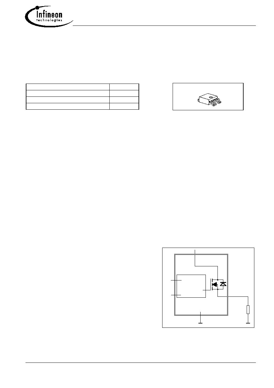
TO 252-5-11
Block Diagram
Vbb
Logic
with
protection
functions
IN
ST
GND
Load
PROFET
OUT
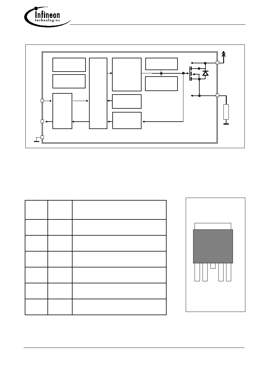
BTS428L2
Infineon Technologies AG
Page 2
2003-Oct-01
Functional diagram
Pin Definitions and Functions
Pin
Symbol
Function
1
GND
Logic ground
2 IN
Input, activates the power switch in
case of logical high signal
3 Vbb
Positive power supply voltage
The tab is shorted to pin 3
4 ST
Diagnostic feedback, low on failure
5 OUT
Output to the load
Tab Vbb
Positive power supply voltage
The tab is shorted to pin 3
Pin configuration
(top view)
Tab = V
BB
1 2 (3) 4 5
GND IN ST OUT
OUT
GND
overvoltage
protection
logic
internal
voltage supply
ESD
temperature
sensor
clamp for
inductive load
gate
control
+
charge
pump
current limit
Open load
detection
ST
VBB
LOAD
IN
PROFET
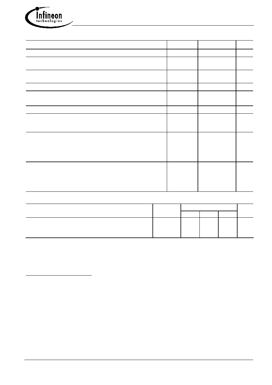
BTS428L2
Infineon Technologies AG
Page 3
2003-Oct-01
Maximum Ratings
at T
j
= 25 °C unless otherwise specified
Parameter Symbol
Values
Unit
Supply voltage
(overvoltage protection see page 4)
V
bb
43
V
Supply voltage for full short circuit protection
T
j Start
=-40 ...+150°C
V
bb
24
V
Load dump protection
1
)
V
LoadDump
= V
A
+ V
s
, V
A
= 13.5 V
R
I
2
)
= 2
, R
L
= 4.0
, t
d
= 200 ms, IN= low or high
V
Load dump
3
)
60
V
Load current
(Current limit, see page 5)
I
L
self-limited
A
Operating temperature range
Storage temperature range
T
j
T
stg
-40 ...+150
-55 ...+150
°C
Power dissipation (DC), T
C
25 °C
P
tot
75
W
Maximal switchable inductance, single pulse
Vbb = 12V, Tj,start = 150°C, TC = 150°C const.
(See diagram on page 9) IL(ISO) = 7 A, RL = 0
;
E
4
)
AS
=0.19J:
Z
L
5.6
mH
Electrostatic discharge capability (ESD)
IN:
(Human Body Model)
ST:
out to all other pins shorted:
acc. MIL-STD883D, method 3015.7 and
ESD assn. std. S5.1-1993; R=1.5k
; C=100pF
V
ESD
1.0
4.0
8.0
kV
Input voltage (DC)
V
IN
-10 ... +16
V
Current through input pin (DC)
Current through status pin (DC)
see internal circuit diagrams page 8
I
IN
I
ST
±
2.0
±
5.0
mA
Thermal Characteristics
Parameter and Conditions Symbol
Values
Unit
min typ max
Thermal resistance
chip - case:
junction - ambient (free air):
device on pcb
5
):
R
thJC
R
thJA
--
--
--
--
--
42
1.67
75
--
K/W
1
) Supply voltages higher than V
bb(AZ)
require an external current limit for the GND and status pins (a 150
resistor for the GND connection is recommended).
2
)
R
I
= internal resistance of the load dump test pulse generator
3
)
V
Load dump
is setup without the DUT connected to the generator per ISO 7637-1 and DIN 40839
4
)
E
AS
is the maximum inductive switch-off energy
5
) Device on 50mm*50mm*1.5mm epoxy PCB FR4 with 6cm
2
(one layer, 70
µ
m thick) copper area for Vbb
connection. PCB is vertical without blown air.
BTS428L2
Infineon Technologies AG
Page 4
2003-Oct-01
Electrical Characteristics
Parameter and Conditions Symbol
Values
Unit
at T
j
=-40...+150°C, V
bb
= 12 V unless otherwise specified
min typ max
Load Switching Capabilities and Characteristics
On-state resistance (pin 3 to 5)
IL = 2 A; V
BB
7V
T
j
=25 °C:
T
j
=150 °C:
see diagram, page 10
R
ON
--
50
100
60
120
m
Nominal load current, (pin 3 to 5)
ISO 10483-1, 6.7:V
ON
=0.5V, T
C
=85°C
I
L(ISO)
5.8
7.0 --
A
Output current (pin
5
) while GND disconnected or
GND pulled up
6
)
, V
bb
=30 V, V
IN
= 0,
see diagram page 8
I
L(GNDhigh)
-- -- 2
mA
Turn-on time
IN
to 90% V
OUT
:
Turn-off time
IN
to 10% V
OUT
:
R
L
= 12
,
t
on
t
off
30
30
100
100
200
200
µ
s
Slew rate on
10 to 30% V
OUT
,
R
L
= 12
,
dV /dt
on
0.1 -- 1 V/
µ
s
Slew rate off
70 to 40% V
OUT
, R
L
= 12
,
-dV/dt
off
0.1 -- 1 V/
µ
s
Operating Parameters
Operating voltage
T
j
=-40
T
j
=+25...+150°C:
V
bb(on)
4.75 --
--
41
43
V
Overvoltage protection
7
)
T
j
=-40°C:
I
bb
=40 mA
T
j
=25...+150°C:
V
bb(AZ)
41
43
--
47
--
52
V
Standby current (pin 3)
8)
T
j
=-40...+25°C
:
V
IN
=0;
see diagram on page 10
T
j
= 150°C:
I
bb(off)
--
--
5
--
9
25
µ
A
Off-State output current (included in I
bb(off)
)
V
IN
=0
I
L(off)
-- 1 10
µ
A
Operating current
9
)
, V
IN
=5 V
I
GND
-- 0.8 1.5
mA
6
) not subject to production test, specified by design
7
)
Supply voltages higher than V
bb(AZ)
require an external current limit for the GND and status pins (a 150
resistor for the GND connection is recommended. See also V
ON(CL)
in table of protection functions and
circuit diagram page 8.
8
) Measured with load
9
)
Add I
ST
, if I
ST
> 0, add I
IN
, if V
IN
>5.5 V
BTS428L2
Parameter and Conditions Symbol
Values
Unit
at T
j
=-40...+150°C, V
bb
= 12 V unless otherwise specified
min typ max
Infineon Technologies AG
Page 5
2003-Oct-01
Protection Functions
10)
Current limit (pin 3 to 5)
I
L(lim)
(see timing diagrams on page 12)
T
j
=-40°C:
T
j
=25°C:
T
j
=+150°C:
21
17
12
28
22
16
36
31
24
A
Repetitive short circuit shutdown current limit
I
L(SCr)
T
j
= T
jt
(see timing diagrams, page 12)
--
17
--
A
Thermal shutdown time
11
T
j,start
= 25°C:
(see timing diagrams on page 12)
t
off(SC)
--
7.5
--
ms
Output clamp (inductive load switch off)
at V
OUT
= V
bb
- V
ON(CL)
I
L
= 40 mA:
V
ON(CL)
41
43
47 52
V
Thermal overload trip temperature
T
jt
150 -- --
°C
Thermal hysteresis
T
jt
-- 10 --
K
Reverse battery (pin 3 to 1)
12
)
-V
bb
--
--
32
V
Reverse battery voltage drop
(V
out
> V
bb
)
13
)
I
L
= -2 A
T
j
=150 °C:
-V
ON(rev)
--
600 --
mV
Diagnostic Characteristics
Open load detection current
(on-condition)
I
L (OL)
10 --
500
mA
10
) Integrated protection functions are designed to prevent IC destruction under fault conditions described in the
data sheet. Fault conditions are considered as "outside" normal operating range. Protection functions are
not designed for continuous repetitive operation.
11
)
Device on 50mm*50mm*1.5mm epoxy PCB FR4 with 6cm
2
(one layer, 70
µ
m thick) copper area for Vbb
connection. PCB is vertical without blown air.
12
)
Requires
150
resistor in GND connection. The reverse load current through the intrinsic drain-source
diode has to be limited by the connected load. Note that the power dissipation is higher compared to normal
operating conditions due to the voltage drop across the intrinsic drain-source diode. The temperature
protection is not active during reverse current operation! Input and Status currents have to be limited (see
max. ratings page 3 and circuit page 8).
13
)
not subject to production test, specified by design