2002-07-25
Page 1
Preliminary data
BSS 192 P
SIPMOS
Small-Signal-Transistor
Product Summary
V
DS
-250
V
R
DS(on)
12
I
D
-0.19
A
Feature
·
P-Channel
·
Enhancement mode
·
Logic Level
·
dv/dt rated
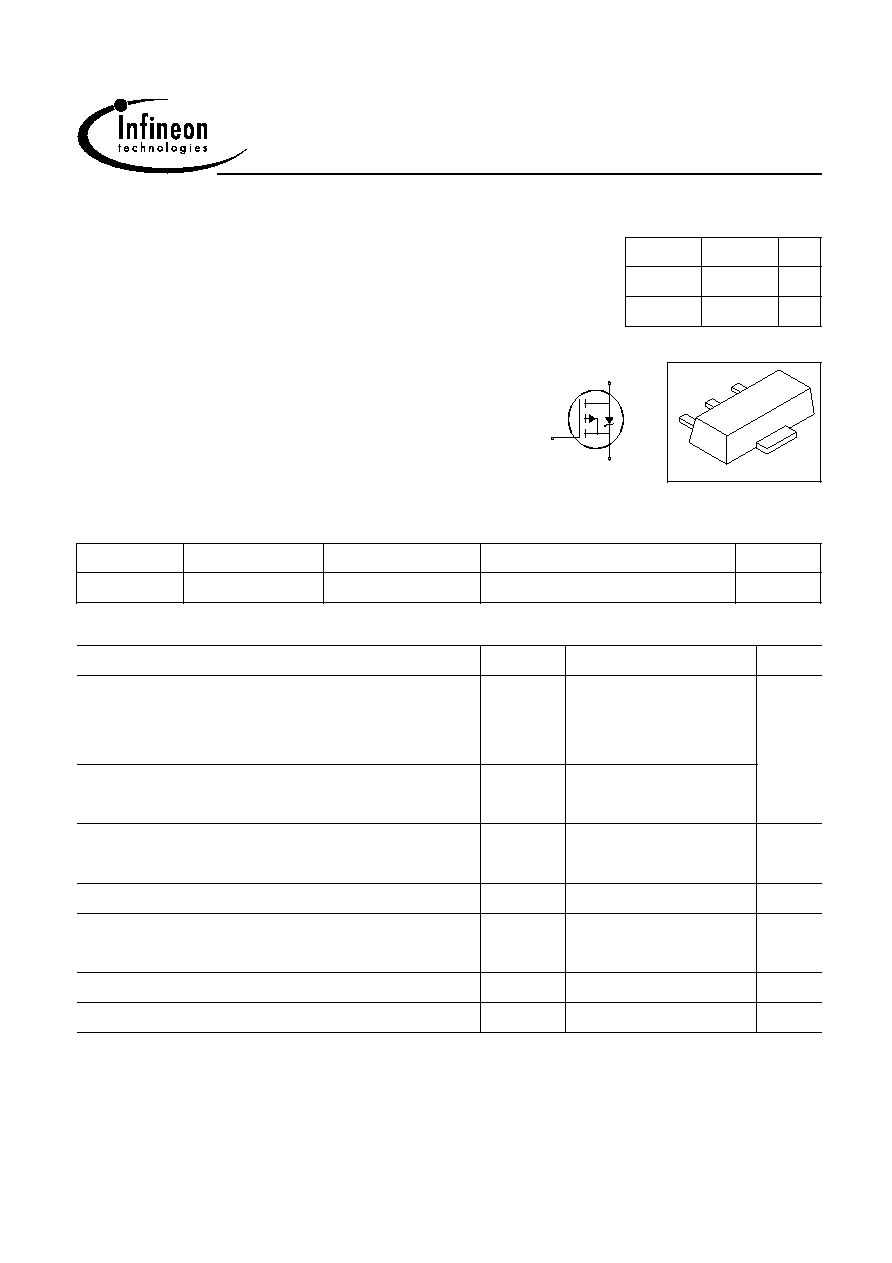
SOT89
2
1
3
VPS05162
2
Gate
pin1
Drain
pin 2
Source
pin 3
Marking
KC
Type
Package
Ordering Code
Tape and Reel Information
BSS 192 P SOT89
Q67042-S4168
-
Maximum Ratings, at T
j
= 25 °C, unless otherwise specified
Parameter
Symbol
Value
Unit
Continuous drain current
TA=25°C
T
A
=70°C
I
D
-0.19
-0.1
A
Pulsed drain current
T
A
=25°C
I
D puls
-0.76
Reverse diode dv/dt
I
S
=-0.19A, V
DS
=-200V, di/dt=-200A/µs, T
jmax
=150°C
dv/dt
6
kV/µs
Gate source voltage
V
GS
±20
V
Power dissipation
TA=25°C
P
tot
1
W
Operating and storage temperature
T
j ,
T
stg
-55... +150
°C
IEC climatic category; DIN IEC 68-1
55/150/56
2002-07-25
Page 2
Preliminary data
BSS 192 P
Thermal Characteristics
Parameter
Symbol
Values
Unit
min.
typ.
max.
Characteristics
Thermal resistance, junction - soldering point
(Pin 2)
R
thJS
-
-
10
K/W
Thermal resistance, junction - ambient, leaded
R
thJA
-
-
125
Electrical Characteristics, at T
j
= 25 °C, unless otherwise specified
Parameter
Symbol
Values
Unit
min.
typ.
max.
Static Characteristics
Drain-source breakdown voltage
V
GS
=0, I
D
=-250µA
V
(BR)DSS
-250
-
-
V
Gate threshold voltage, V
GS
= V
DS
I
D
=-130µA
V
GS(th)
-1
-1.5
-2
Zero gate voltage drain current
V
DS
=-250V, V
GS
=0, T
j
=25°C
V
DS
=-250V, V
GS
=0, T
j
=150°C
I
DSS
-
-
-0.1
-10
-0.2
-100
µA
Gate-source leakage current
V
GS
=-20V, V
DS
=0
I
GSS
-
-10
-100
nA
Drain-source on-state resistance
V
GS
=-2.8V, I
D
=-0.025A
R
DS(on)
-
10
20
Drain-source on-state resistance
V
GS
=-4.5V, I
D
=-0.1A
R
DS(on)
-
8.3
15
Drain-source on-state resistance
V
GS
=-10V, I
D
=-0.19A
R
DS(on)
-
7.7
12

2002-07-25
Page 3
Preliminary data
BSS 192 P
Electrical Characteristics, at T
j
= 25 °C, unless otherwise specified
Parameter
Symbol
Conditions
Values
Unit
min.
typ.
max.
Dynamic Characteristics
Transconductance
g
fs
|V
DS
|
2*|I
D
|*R
DS(on)max
,
I
D
=-0.1A
0.19
0.38
-
S
Input capacitance
C
iss
V
GS
=0, V
DS
=-25V,
f=1MHz
-
83
104
pF
Output capacitance
C
oss
-
13
16
Reverse transfer capacitance
C
rss
-
6
8
Turn-on delay time
t
d(on)
V
DD
=-125V, V
GS
=-10V,
I
D
=-0.19A, R
G
=2
-
4.7
7
ns
Rise time
t
r
-
5.2
8
Turn-off delay time
t
d(off)
-
72
108
Fall time
t
f
-
50
75
Gate Charge Characteristics
Gate to source charge
Q
gs
V
DD
=-200V, I
D
=-0.19A
-
-0.2
-0.25 nC
Gate to drain charge
Q
gd
-
-1.9
-2.4
Gate charge total
Q
g
V
DD
=-200V, I
D
=-0.19A,
V
GS
=0 to -10V
-
-4.9
-6.1
Gate plateau voltage
V
(plateau) V
DD
=-200V, I
D
=-0.19A
-
-2.63
-
V
Reverse Diode
Inverse diode continuous
forward current
I
S
T
A
=25°C
-
-
-0.19 A
Inv. diode direct current, pulsed I
SM
-
-
-0.76
Inverse diode forward voltage V
SD
V
GS
=0, I
F
=-0.19A
-
-0.78
-1.1
V
Reverse recovery time
t
rr
V
R
=-125V, I
F=
l
S
,
di
F
/dt=100A/µs
-
46
57
ns
Reverse recovery charge
Q
rr
-
72
90
nC

2002-07-25
Page 4
Preliminary data
BSS 192 P
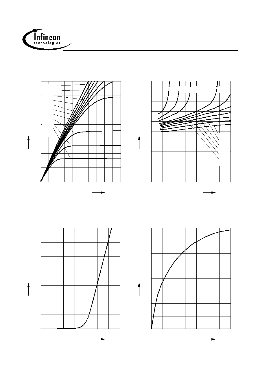
1 Power dissipation
P
tot
= f (TA)
0
20
40
60
80
100
120
°C
160
T
A
0
0.1
0.2
0.3
0.4
0.5
0.6
0.7
0.8
0.9
W
1.1
BSS 192 P
P
tot
2 Drain current
I
D
= f (TA)
parameter: |V
GS
|
10V
0
20
40
60
80
100
120
°C
160
T
A
0
-0.02
-0.04
-0.06
-0.08
-0.1
-0.12
-0.14
-0.16
A
-0.2
BSS 192 P
I
D
3 Safe operating area
I
D
= f ( V
DS
)
parameter : D = 0 , TA = 25°C
-10
-1
-10
0
-10
1
-10
2
-10
3
V
V
DS
-3
-10
-2
-10
-1
-10
0
-10
1
-10
A
BSS 192 P
I
D
R
D
S(
on
)
=
V
D
S
/
I
D
DC
10 ms
1 ms
tp = 240.0µs
4 Transient thermal impedance
Z
thJA
= f (t
p
)
parameter : D = t
p
/T
10
-7
10
-6
10
-5
10
-4
10
-3
10
-2
10
0
s
t
p
-4
10
-3
10
-2
10
-1
10
0
10
1
10
2
10
3
10
K/W
BSS 192 P
Z
thJA
single pulse
0.01
0.02
0.05
0.10
0.20
D = 0.50
2002-07-25
Page 5
Preliminary data
BSS 192 P
5 Typ. output characteristic
I
D
= f (V
DS
)
parameter: Tj =25°C, -V
GS
0
1
2
3
4
5
6
7
8
V
10
-V
DS
0
0.1
0.2
0.3
0.4
0.5
A
0.7
-
I
D
10V
6V
4.6V
4V
3.6V
3.4V
3.2V
2.8V
2.6V
2.4V
6 Typ. drain-source on resistance
R
DS(on)
= f (I
D
)
parameter: V
GS
; Tj =25°C, -V
GS
0
0.1
0.2
0.3
0.4
0.5
A
0.7
-I
D
0
1.5
3
4.5
6
7.5
9
10.5
12
15
R
DS(on)
2.4V 2.6V
2.8V
3.2V
10V
6V
4.6V
4V
3.6V
3.4V
7 Typ. transfer characteristics
I
D
= f ( V
GS
); |V
DS|
2 x |I
D
| x R
DS(on)max
parameter: T
j
= 25 °C
0
0.5
1
1.5
2
2.5
V
3.5
-V
GS
0
0.1
0.2
0.3
0.4
0.5
A
0.7
-
I
D
8 Typ. forward transconductance
g
fs
= f(I
D
)
parameter: Tj =25°C
0
0.1
0.2
0.3
0.4
0.5
A
0.7
-I
D
0
0.1
0.2
0.3
0.4
0.5
0.6
S
0.8
g
fs