miniPROFET
Û
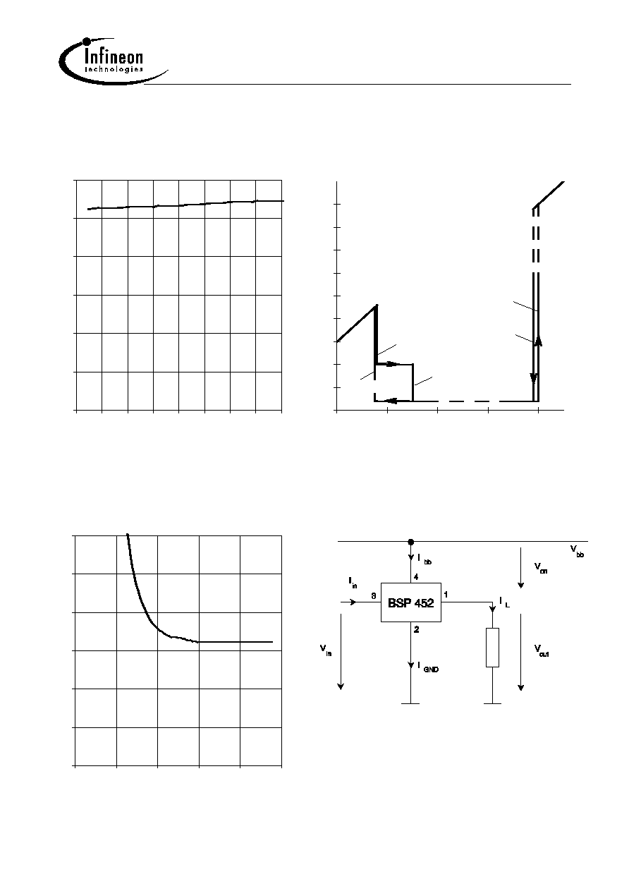
BSP 452
Data Book
1 20.08.96
ñ
High-side switch
ñ
Short-circuit protection
ñ
Input protection
ñ
Overtemperature protection with hysteresis
ñ
Overload protection
ñ
Overvoltage protection
ñ
Switching inductive load
ñ
Clamp of negative output voltage with inductive loads
ñ
Undervoltage shutdown
ñ
Maximum current internally limited
ñ
Electrostatic discharge (ESD) protection
ñ
Reverse battery protection
1
)
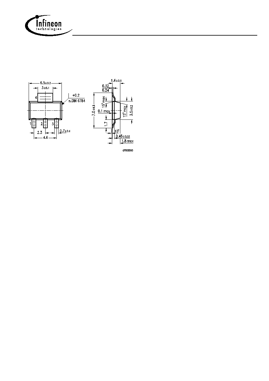
Package: SOT 223
Type
Ordering code
BSP 452
Q67000-S271
Application
ñ
ç
C compatible power switch for 12 V DC grounded loads
ñ
All types of resistive, inductive and capacitive loads
ñ
Replaces electromechanical relays and discrete circuits
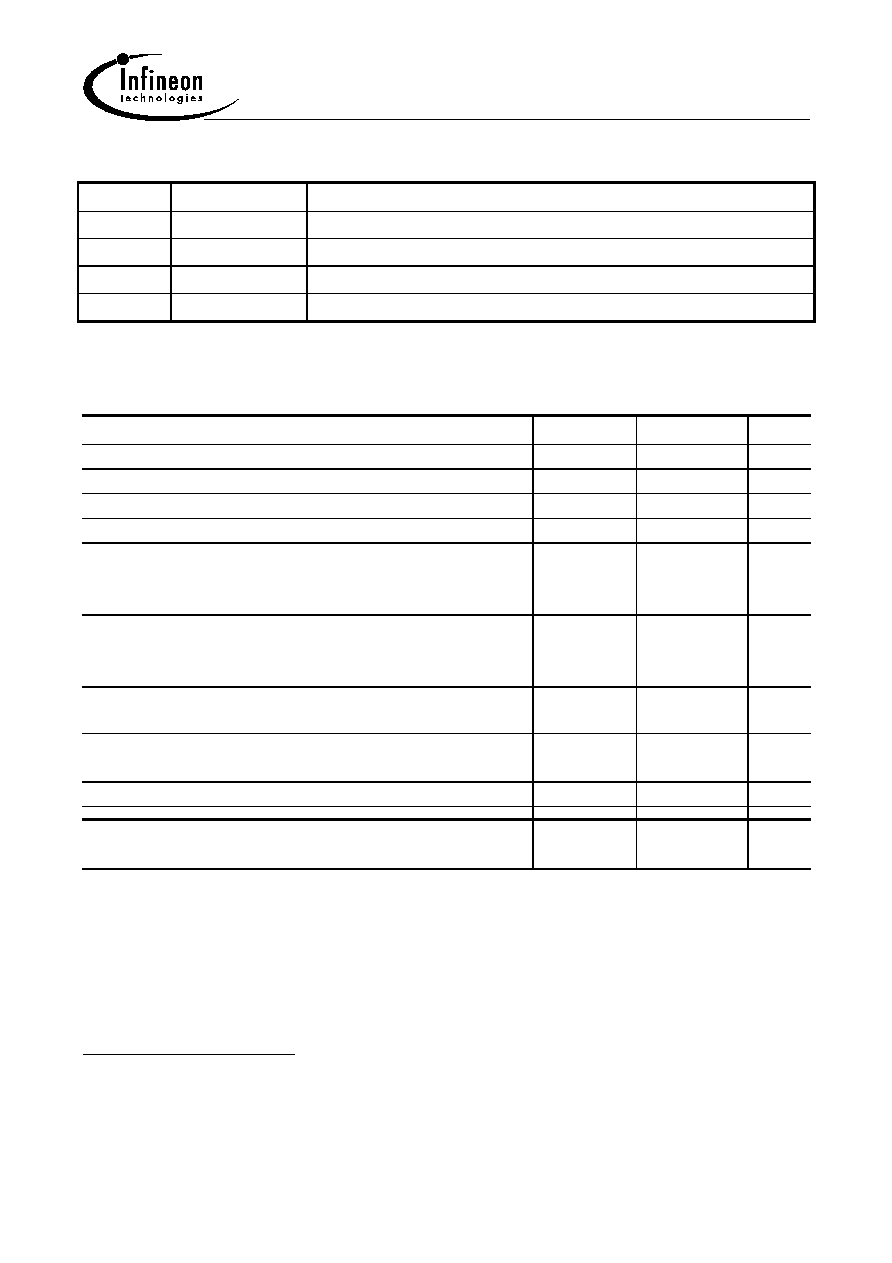
General Description
N channel vertical power FET with charge pump, ground referenced CMOS compatible input,monolithically
integrated in Smart SIPMOS
technology. Fully protected by embedded protection functions.
Blockdiagramm:
IN
3
R
in
+ Vbb
Signal GND
ESD
miniPROFET
OUT
GND
Logic
Voltage
sensor
Voltage
source
Charge pump
Level shifter
Temperature
sensor
Rectifier
Limit for
unclamped
ind. loads
Gate
protection
Current
limit
2
4
1
Load GND
Load
V
Logic
Overvoltage
protection
ESD-
Diode
1
) With resistor RGND=150
in GND connection, resistor in series with IN connections reverse load current
limited by connected load.
SOT-223
SOT-223
1
miniPROFET
Û
BSP 452
Data Book
2 20.08.96
Pin
Symbol
Function
1
OUT
O
Output to the load
2
GND
-
Logic ground
3
IN
I
Input, activates the power switch in case of logical high signal
4
Vbb
+
Positive power supply voltage
Maximum Ratings
at
T
j
= 25 ¯C unless otherwise specified
Parameter
Symbol
Values
Unit
Supply voltage
V
bb
40
V
Load current
self-limited
I
L
I
L(SC)
A
Maximum input voltage
2)
V
IN
-5.0...
V
bb
V
Maximum input current
I
IN
Ý
5
mA
Inductive load switch-off energy dissipation,
single pulse
I
L
= 0.5A ,
T
A
= 150¯C
(not tested, specified by design)
E
AS
0.5
J
Load dump protection
3
)
V
LoadDump
=
U
A
+
V
s
R
L
= 24
R
I
=2
,
t
d
=400ms, IN= low or high,
U
A
=13,5V
R
L
= 80
(not tested, specified by design)
V
Load dump
4
)
60
80
V
Electrostatic discharge capability (ESD)
5)
PIN 3
PIN 1,2,4
V
ESD
Ý
1
Ý
2
kV
Operating temperature range
Storage temperature range
T
j
T
stg
-40 ...+150
-55 ...+150
¯C
Max. power dissipation (DC)
6)
T
A
= 25 ¯C
P
tot
1.8
W
Thermal resistance
chip - soldering point:
chip - ambient:
6)
R
thJS
R
thJA
7
70
K/W
2
) At V
IN > Vbb, the input current is not allowed to exceed
Ý
5 mA.
3
)
Supply voltages higher than Vbb(AZ) require an external current limit for the GND pin, e.g. with a 150
resistor in the GND connection
A resistor for the protection of the input is integrated.
4
)
VLoad dump is setup without the DUT connected to the generator per ISO 7637-1 and DIN 40839
5
)
HBM according to MIL-STD 883D, Methode 3015.7
6
) BSP 452 on epoxy pcb 40 mm x 40 mm x 1.5 mm with 6 cm2 copper area for V
bb connection
miniPROFET
Û
BSP 452
Data Book
3 20.08.96
Electrical Characteristics
Parameter and Conditions
Symbol
Values
Unit
at
T
j
= 25 ¯C,
Vbb = 13.5V unless otherwise specified
min
typ
max
Load Switching Capabilities and Characteristics
On-state resistance (pin 4 to 1)
I
L
= 0.5 A,
V
in
= high
T
j
= 25¯C
T
j
= 150¯C
R
ON
--
--
0.16
--
0.2
0.4
Nominal load current (pin 4 to 1)
7)
ISO Standard:
V
ON
=
V
bb
-
V
OUT
= 0.5 V
T
S
= 85 ¯C
I
L(ISO)
0.7
--
--
A
Turn-on time
to 90%
V
OUT
Turn-off time
to 10%
V
OUT
R
L
= 24
t
on
t
off
--
--
60
60
100
150
ç
s
Slew rate on
10 to 30%
V
OUT
,
R
L
= 24
d
V
/dt
on
--
2
4
V/
ç
s
Slew rate off
70 to 40%
V
OUT
,
R
L
= 24
-d
V
/dt
off
--
2
4
V/
ç
s
Input
Allowable input voltage range, (pin 3 to 2)
V
IN
-3.0
--
V
bb
V
Input turn-on threshold voltage
T
j
= -40...+150¯C
V
IN(T+)
--
--
3.5
V
Input turn-off threshold voltage
T
j
= -40...+150¯C
V
IN(T-)
1.5
--
--
V
Input threshold hysteresis
V
IN(T)
--
0.5
--
V
Off state input current (pin 3)
V
IN(off)
= 1.2 V
T
j
= -40...+150¯C
I
IN(off)
10
--
60
ç
A
On state input current (pin 3)
V
IN(on)
= 3.0 V to
V
bb
T
j
= -40...+150¯C
I
IN(on)
10
--
100
ç
A
Input resistance
R
IN
1.5
2.8
3.5
k
7
)
I
L(ISO) is limited by current limitation, see
I
L(SC)
, next page

miniPROFET
Û
BSP 452
Data Book
4 20.08.96
Parameter and Conditions
Symbol
Values
Unit
at
T
j
= 25 ¯C,
Vbb = 13.5V unless otherwise specified
min
typ
max
Operating Parameters
Operating voltage
8
)
T
j
=-40...+150¯C
V
bb(on)
5.0
--
34
V
Undervoltage shutdown
T
j
=-40...+150¯C
V
bb(under)
3.5
--
5
V
Undervoltage restart
T
j
=-40...+25¯C
T
j
=+150¯C
V
bb(u rst)
--
--
6.5
7.0
V
Undervoltage restart of charge pumpe
see diagram page 7
V
bb(ucp)
--
5.6
7
V
Undervoltage hysteresis
V
bb(under)
=
V
bb(u rst)
-
V
bb(under)
V
bb(under)
--
0.3
--
V
Overvoltage shutdown
T
j
=-40...+150¯C
V
bb(over)
34
--
42
V
Overvoltage restart
T
j
=-40...+150¯C
V
bb(o rst)
33
--
--
V
Overvoltage hysteresis
T
j
=-40...+150¯C
V
bb(over)
--
0.7
--
V
Standby current (pin 4),
V
in
= low
T
j
=-40...+150¯C
I
bb(off)
--
10
25
ç
A
Operating current (pin 2),
V
in
= 5 V
I
GND
--
1
1.6
mA
leakage current (pin 1)
V
in
= low
T
j
=-40...+25¯C
T
j
=150¯C
I
L(off)
--
2
5
7
ç
A
Protection Functions
Current limit (pin 4 to 1)
T
j
= 25¯C
V
bb
= 20V
T
j
= -40...+150¯C
I
L(SC)
0.7
0.7
1.5
--
2
2.4
A
Overvoltage protection
I
bb=4mA
T
j
=-40...+150¯C
V
bb(AZ)
41
--
--
V
Output clamp (ind. load switch off)
at
V
OUT
=
V
bb
-
V
ON(CL),
I
bb
= 4mA
V
ON(CL)
41
47
--
V
Thermal overload trip temperature
T
jt
150
--
--
¯C
Thermal hysteresis
T
jt
--
10
--
K
Inductive load switch-off energy dissipation
9
)
T
j Start
= 150 ¯C, single pulse,
I
L
= 0.5 A,
V
bb
= 12 V
(not tested, specified by design)
E
AS
--
--
0.5
J
Reverse battery (pin 4 to 2)
10
)
(not tested, specified by design)
-
V
bb
--
--
30
V
8
)
At supply voltage increase up to
V
bb= 5.6 V typ without charge pump,
V
OUT
V
bb - 2 V
9
)
While demagnetizing load inductance, dissipated energy in PROFET is
E
AS=
V
ON(CL) *
i
L(t) dt, approx.
E
AS=
1/
2 *
L
*
I
2
L
* (
V
ON(CL)
V
ON(CL) -
V
bb
)
10
) Requires 150
resistor in GND connection. Reverse load current (through intrinsic drain-source diode) is normally limited by the
connected load.
7
miniPROFET
Û
BSP 452
Data Book
5 20.08.96
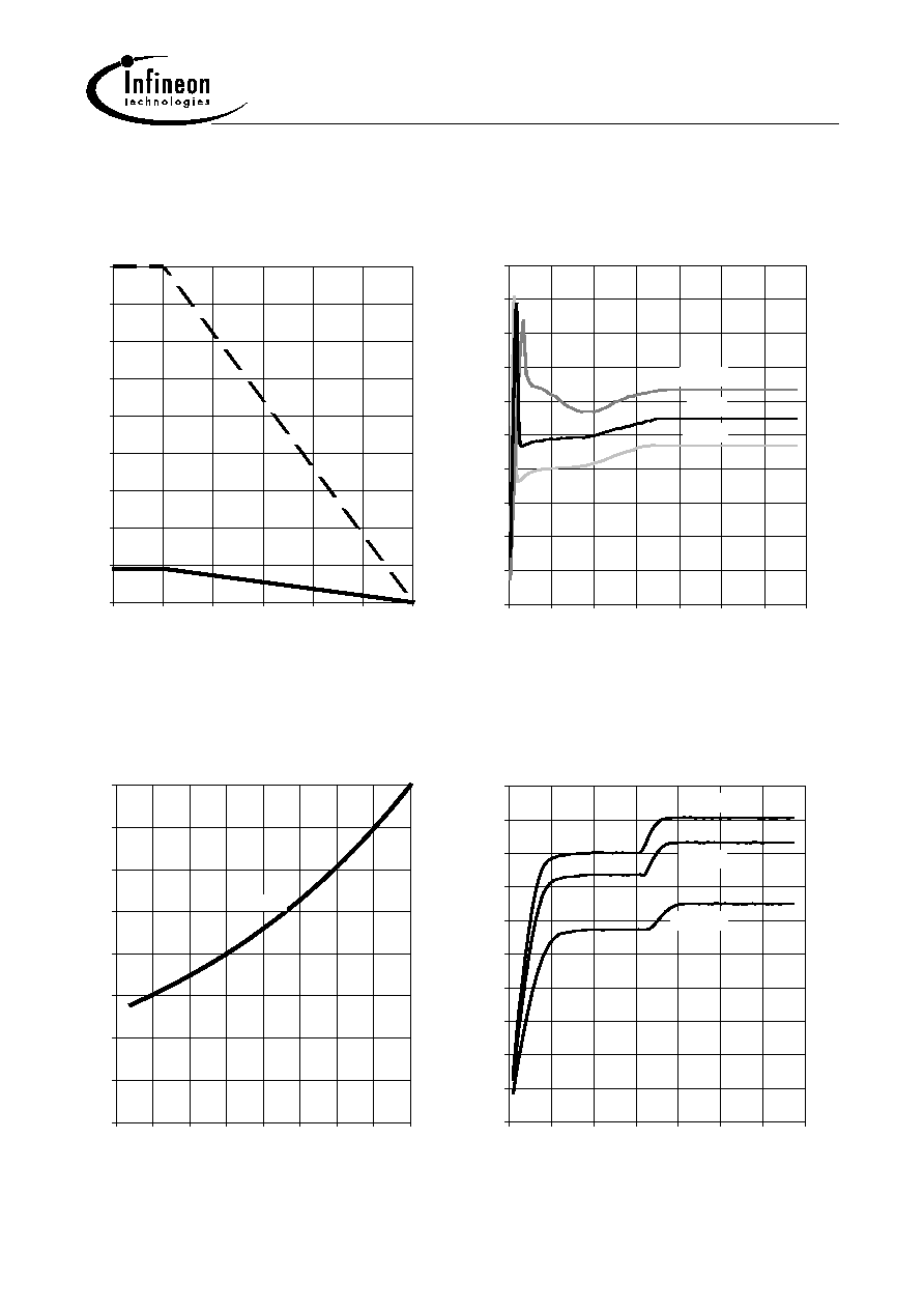
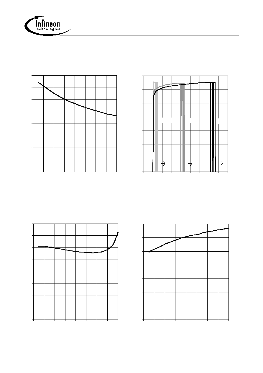
Max. allowable power dissipation
Ptot = f (TA,TSP)
Ptot [W]
0
2
4
6
8
10
12
14
16
18
0
25
50
75
100
125
150
T
A
T
SP
TA, TSP[¯C]
On state resistance (Vbb-pin to OUT-pin)
RON = f (Tj); Vbb = 13.5 V; IL = 0.5 A
RON [
]
0
0.05
0.1
0.15
0.2
0.25
0.3
0.35
0.4
-50
-25
0
25
50
75
100
125
150
98%
Tj [¯C]
Current limit characteristic
IL(SC) = f (Von); (Von see testcircuit)
IL(SC) [A]
0
0.2
0.4
0.6
0.8
1
1.2
1.4
1.6
1.8
2
0
2
4
6
8
10
12
14
25¯C
150¯C
-40¯C
Von [V]
Typ. input current
IIN = f (VIN); Vbb = 13,5 V
IIN [çA]
0
5
10
15
20
25
30
35
40
45
50
0
2
4
6
8
10
12
14
-40¯C
+150¯C
+ 25¯C
VIN [V]
miniPROFET
Û
BSP 452
Data Book
6 20.08.96
Typ. operating current
IGND = f (Tj); Vbb = 13,5 V; VIN = high
IGND [mA]
0
0.1
0.2
0.3
0.4
0.5
0.6
0.7
0.8
-50
-25
0
25
50
75
100
125
150
Tj [¯C]
Typ. standby current
Ibb(off) = f (Tj); Vbb = 13,5 V; VIN = low
Ibb(off) [çA]
0
1
2
3
4
5
6
7
8
-50
-25
0
25
50
75
100
125
150
Tj [¯C]
Typ. overload current
IL(lim) = f (t); Vbb = 13,5 V, no heatsink, Param.: Tjstart
IL(lim) [A]
0
0.2
0.4
0.6
0.8
1
1.2
1.4
-50
0
50
100
150
200
250
300
350
400
-40¯C
+150¯C
+25¯C
t [ms]
Short circuit current
IL(SC) = f (Tj); Vbb = 13,5 V
IL(SC) [A]
0
0.2
0.4
0.6
0.8
1
1.2
1.4
-50
-25
0
25
50
75
100
125
150
Tj [¯C]
miniPROFET
Û
BSP 452
Data Book
7 20.08.96
Typ. input turn on voltage threshold
VIN(T+) = f (Tj);
VIN(T+) [V]
0
0.5
1
1.5
2
2.5
3
-50
-25
0
25
50
75
100
125
150
13V
Tj [¯C]
Typ. on-state resistance (Vbb-Pin to Out-Pin)
RON = f (Vbb,IL); IL=0.5A, Tj = 25¯C
RON [m
]
0
5 0
1 0 0
1 5 0
2 0 0
2 5 0
3 0 0
0
5
1 0
1 5
2 0
2 5
Vbb [V]
Figure 6: Undervoltage restart of charge pumpe
V
ON
[V]
V
bb(under)
V
bb(u rs t)
V
bb(over)
V
bb(o rs t)
V
bb(u c p)
V
bb
[V]
charge pump starts at V
bb(ucp)
about 7 V typ.
Test circuit
m
ini
PROFETÛ BSP 452
Semiconductor Group
8
20.08.96
Package:
all dimensions in mm.
SOT 223/4:
Published by
Infineon Technologies AG,
St.-Martin-Strasse 53,
D-81669 M■nchen
ˋ Infineon Technologies AG 2001
All Rights Reserved.
Attention please!
The information herein is given to describe certain components and shall not be considered as a guarantee of characteristics.
Terms of delivery and rights to technical change reserved.
We hereby disclaim any and all warranties, including but not limited to warranties of non-infringement, regarding circuits,
descriptions and charts stated herein.
Infineon Technologies is an approved CECC manufacturer.
Information
For further information on technology, delivery terms and conditions and prices please contact your nearest Infineon
Technologies Office in Germany or our Infineon Technologies Representatives worldwide (see address list).
Warnings
Due to technical requirements components may contain dangerous substances. For information on the types in question please
contact your nearest Infineon Technologies Office.
Infineon Technologies Components may only be used in life-support devices or systems with the express written approval of
Infineon Technologies, if a failure of such components can reasonably be expected to cause the failure of that life-support
device or system, or to affect the safety or effectiveness of that device or system. Life support devices or systems are intended
to be implanted in the human body, or to support and/or maintain and sustain and/or protect human life. If they fail, it is
reasonable to assume that the health of the user or other persons may be endangered.