
2002-12-10
Page 1
Rev. 1.0
BSP296
SIPMOS
Small-Signal-Transistor
Product Summary
V
DS
100
V
R
DS(on)
0.7
I
D
1.1
A
Feature
·
N-Channel
·
Enhancement mode
·
Logic Level
·
dv/dt rated
SOT-223
VPS05163
1
2
3
4
Marking
BSP296
Type
Package
Ordering Code
Tape and Reel Information
BSP296
SOT-223
Q67000-S067
E6327
Maximum Ratings, at
T
j
= 25 °C, unless otherwise specified
Parameter
Symbol
Value
Unit
Continuous drain current
T
A
=25°C
T
A
=70°C
I
D
1.1
0.88
A
Pulsed drain current
T
A
=25°C
I
D puls
4.4
Reverse diode dv/dt
I
S
=1.1A, V
DS
=80V, di/dt=200A/µs, T
jmax
=150°C
dv/dt
6
kV/µs
Gate source voltage
V
GS
±20
V
ESD Sensitivity (HBM) as per MIL-STD 883
Class 1
Power dissipation
T
A
=25°C
P
tot
1.79
W
Operating and storage temperature
T
j ,
T
stg
-55... +150
°C
IEC climatic category; DIN IEC 68-1
55/150/56

2002-12-10
Page 2
Rev. 1.0
BSP296
Thermal Characteristics
Parameter
Symbol
Values
Unit
min.
typ.
max.
Characteristics
Thermal resistance, junction - soldering point
(Pin 4)
R
thJS
-
-
25
K/W
SMD version, device on PCB:
@ min. footprint
@ 6 cm
2
cooling area
1)
R
thJA
-
-
-
-
115
70
Electrical Characteristics, at
T
j
= 25 °C, unless otherwise specified
Parameter
Symbol
Values
Unit
min.
typ.
max.
Static Characteristics
Drain-source breakdown voltage
V
GS
=0, I
D
=250µA
V
(BR)DSS
100
-
-
V
Gate threshold voltage,
V
GS
=
V
DS
I
D
=400µA
V
GS(th)
0.8
1.4
1.8
Zero gate voltage drain current
V
DS
=100V, V
GS
=0, T
j
=25°C
V
DS
=100V, V
GS
=0, T
j
=150°C
I
DSS
-
-
-
-
0.1
50
µA
Gate-source leakage current
V
GS
=20V, V
DS
=0
I
GSS
-
10
100
nA
Drain-source on-state resistance
V
GS
=4.5V, I
D
=0.95A
R
DS(on)
-
0.62
1
Drain-source on-state resistance
V
GS
=10V, I
D
=1.1A
R
DS(on)
-
0.43
0.7
1Device on 40mm*40mm*1.5mm epoxy PCB FR4 with 6cm˛ (one layer, 70 µm thick) copper area for drain
connection. PCB is vertical without blown air.

2002-12-10
Page 3
Rev. 1.0
BSP296
Electrical Characteristics, at
T
j
= 25 °C, unless otherwise specified
Parameter
Symbol
Conditions
Values
Unit
min.
typ.
max.
Dynamic Characteristics
Transconductance
g
fs
V
DS
2*I
D
*R
DS(on)max
,
I
D
=0.88A
0.6
1.2
-
S
Input capacitance
C
iss
V
GS
=0, V
DS
=25V,
f=1MHz
-
291
364
pF
Output capacitance
C
oss
-
53
66
Reverse transfer capacitance
C
rss
-
29
36
Turn-on delay time
t
d(on)
V
DD
=50V, V
GS
=10V,
I
D
=1.1A, R
G
=6
-
5.2
7.8
ns
Rise time
t
r
-
7.9
11.8
Turn-off delay time
t
d(off)
-
37.4
56.1
Fall time
t
f
-
21.4
32.1
Gate Charge Characteristics
Gate to source charge
Q
gs
V
DD
=80V, I
D
=1.1A
-
0.7
0.9
nC
Gate to drain charge
Q
gd
-
5
7.5
Gate charge total
Q
g
V
DD
=80V, I
D
=1.1A,
V
GS
=0 to 10V
-
13.8
17.2
Gate plateau voltage
V
(plateau) V
DD
=80V, I
D
= 1.1 A
-
2.7
-
V
Reverse Diode
Inverse diode continuous
forward current
I
S
T
A
=25°C
-
-
1.1
A
Inv. diode direct current, pulsed
I
SM
-
-
4.4
Inverse diode forward voltage
V
SD
V
GS
=0, I
F
= I
S
-
0.82
1.2
V
Reverse recovery time
t
rr
V
R
=50V, I
F=
l
S
,
di
F
/dt=100A/µs
-
44.3
55.4
ns
Reverse recovery charge
Q
rr
-
71.9
89.8
nC
2002-12-10
Page 4
Rev. 1.0
BSP296
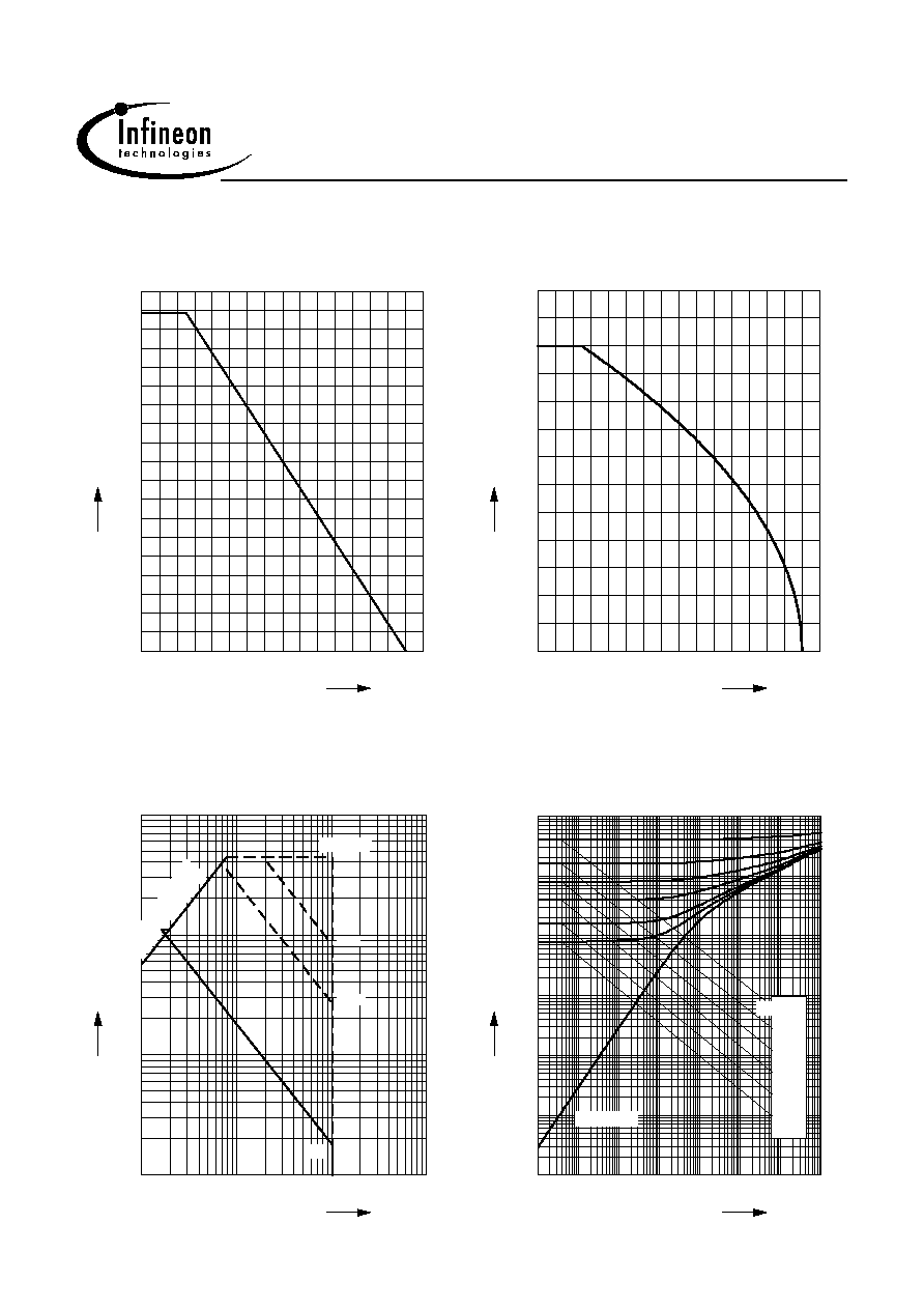
1 Power dissipation
P
tot
= f (
T
A
)
0
20
40
60
80
100
120
°C
160
T
A
0
0.2
0.4
0.6
0.8
1
1.2
1.4
1.6
W
1.9
BSP296
P
tot
2 Drain current
I
D
= f (
T
A
)
parameter: V
GS
10 V
0
20
40
60
80
100
120
°C
160
T
A
0
0.1
0.2
0.3
0.4
0.5
0.6
0.7
0.8
0.9
1
1.1
A
1.3
BSP296
I
D
3 Safe operating area
I
D
= f ( V
DS
)
parameter : D = 0 ,
T
A
= 25 °C
10
0
10
1
10
2
10
3
V
V
DS
-2
10
-1
10
0
10
1
10
A
BSP296
I
D
R
D
S
(o
n)
=
V
D
S
/
I
D
DC
10 ms
1 ms
t
p = 120.0µs
4 Transient thermal impedance
Z
thJA
= f (t
p
)
parameter : D = t
p
/T
10
-7
10
-6
10
-5
10
-4
10
-3
10
-2
10
0
s
t
p
-4
10
-3
10
-2
10
-1
10
0
10
1
10
2
10
K/W
BSP296
Z
thJA
single pulse
0.01
0.02
0.05
0.10
0.20
D = 0.50
2002-12-10
Page 5
Rev. 1.0
BSP296
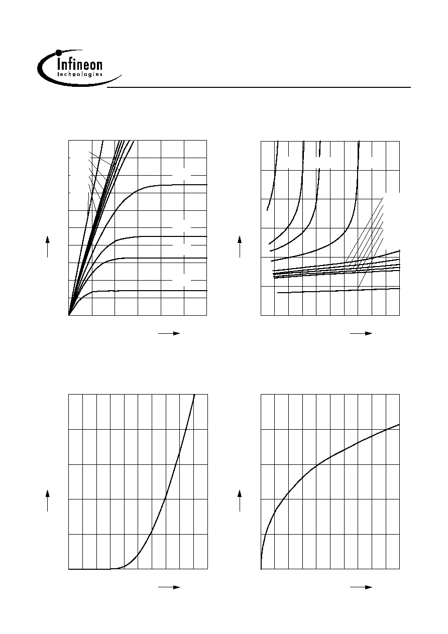
5 Typ. output characteristic
I
D
= f (
V
DS
)
parameter: T
j
= 25 °C, V
GS
0
0.5
1
1.5
2
V
3
V
DS
0
0.2
0.4
0.6
0.8
1
1.2
1.4
1.6
A
2
I
D
2.1V
2.5V
2.7V
3.1V
3.7V
3.9V
4.1V
4.3V
4.5V
10V
6 Typ. drain-source on resistance
R
DS(on)
= f (I
D
)
parameter: T
j
= 25 °C,
V
GS
0
0.2 0.4
0.6
0.8
1
1.2
1.4
1.6
A
2
I
D
0.2
0.5
0.8
1.1
1.4
2
R
DS(on)
2.1V
2.5V 2.7V
3.1V
3.7V
3.9V
4.5V
5V
6V
10V
7 Typ. transfer characteristics
I
D
= f ( V
GS
); V
DS
2 x I
D
x R
DS(on)max
parameter: T
j
= 25 °C
0
0.4
0.8
1.2 1.6
2
2.4 2.8
3.2
V
4
V
GS
0
0.4
0.8
1.2
A
2
I
D
8 Typ. forward transconductance
g
fs
= f(I
D
)
parameter: T
j
= 25 °C
0
0.2 0.4
0.6
0.8
1
1.2
1.4
1.6
A
2
I
D
0
0.4
0.8
1.2
S
2
g
fs