BSP135
SIPMOS
®
Small-Signal-Transistor
Features
· N-channel
· Depletion mode
· dv /dt rated
Maximum ratings, at T
j
=25 °C, unless otherwise specified
Parameter
Symbol Conditions
Unit
Continuous drain current
I
D
T
A
=25 °C
0.12
A
T
A
=70 °C
0.10
Pulsed drain current
I
D,pulse
T
A
=25 °C
0.48
Reverse diode dv /dt
dv /dt
I
D
=0.12 A, V
DS
=20 V,
di /dt =200 A/µs,
T
j,max
=150 °C
6
kV/µs
Gate source voltage
V
GS
±20
V
ESD sensitivity (HBM) as per
MIL-STD 883
Class 1
Power dissipation
P
tot
T
A
=25 °C
1.8
W
Operating and storage temperature
T
j
, T
stg
-55 ... 150
°C
IEC climatic category; DIN IEC 68-1
55/150/56
Value
V
DS
600
V
R
DS(on),max
60
I
DSS,min
0.02
A
Product Summary
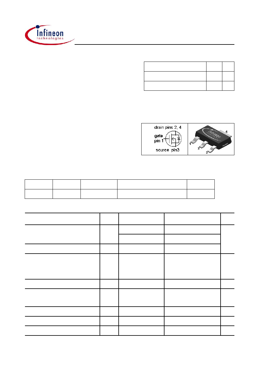
Type
Package
Ordering Code
Tape and Reel Information
Marking
BSP135
SOT-223
Q62702-S655
E6327: 1000 pcs/reel
BSP135
SOT-223
Rev. 1.0
page 1
2003-04-03
BSP135
Parameter
Symbol Conditions
Unit
min.
typ.
max.
Thermal characteristics
Thermal resistance,
junction - soldering point (pin 4)
R
thJS
-
-
25
K/W
SMD version, device on PCB
R
thJA
minimal footprint
-
-
115
6 cm
2
cooling area
1)
-
-
70
Electrical characteristics, at T
j
=25 °C, unless otherwise specified
Static characteristics
Drain-source breakdown voltage
V
(BR)DSS
V
GS
=-3 V, I
D
=250 µA
600
-
-
V
Gate threshold voltage
V
GS(th)
V
DS
=3 V, I
D
=94 µA
-2.1
-1.4
-1
Drain-source cutoff current
I
D(off)
V
DS
=600 V,
V
GS
=-3 V, T
j
=25 °C
-
-
0.1
µA
V
DS
=600 V,
V
GS
=-3 V, T
j
=125 °C
-
-
10
Gate-source leakage current
I
GSS
V
GS
=20 V, V
DS
=0 V
-
-
100
nA
On-state drain current
I
DSS
V
GS
=0 V, V
DS
=10 V
20
-
-
mA
Drain-source on-state resistance
R
DS(on)
V
GS
=0 V, I
D
=0.01A
-
30
60
V
GS
=10 V, I
D
=0.12 A
-
25
45
Transconductance
g
fs
|V
DS
|>2|I
D
|R
DS(on)max
,
I
D
=0.1 A
0.08
0.16
-
S
Values
1)
Device on 40 mm x 40 mm x 1.5 mm epoxy PCB FR4 with 6 cm
2
(single layer, 70 µm thick) copper area for drain
connection. PCB is vertical in still air.
Rev. 1.0
page 2
2003-04-03
BSP135
Parameter
Symbol Conditions
Unit
min.
typ.
max.
Dynamic characteristics
Input capacitance
C
iss
-
98
146
pF
Output capacitance
C
oss
-
8.5
13
Reverse transfer capacitance
C
rss
-
3.4
5.1
Turn-on delay time
t
d(on)
-
5.4
8.1
ns
Rise time
t
r
-
5.6
8.4
Turn-off delay time
t
d(off)
-
28
42
Fall time
t
f
-
182
273
Gate Charge Characteristics
Gate to source charge
Q
gs
-
0.24
0.36
nC
Gate to drain charge
Q
gd
-
2.0
3.0
Gate charge total
Q
g
-
3.7
4.9
Gate plateau voltage
V
plateau
-
0.20
-
V
Reverse Diode
Diode continous forward current
I
S
-
-
0.12
A
Diode pulse current
I
S,pulse
-
-
0.48
Diode forward voltage
V
SD
V
GS
=-3 V, I
F
=0.12 A,
T
j
=25 °C
-
0.78
1.2
V
Reverse recovery time
t
rr
-
87
130
ns
Reverse recovery charge
Q
rr
-
70
104
nC
V
R
=300 V, I
F
=0.1 A,
di
F
/dt =100 A/µs
T
A
=25 °C
Values
V
GS
=-3 V, V
DS
=25 V,
f =1 MHz
V
DD
=300 V,
V
GS
=-3...5 V,
I
D
=0.1 A, R
G
=6
V
DD
=400 V, I
D
=0.1 A,
V
GS
=-3 to 5 V
Rev. 1.0
page 3
2003-04-03
BSP135
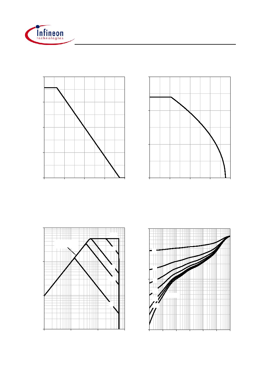
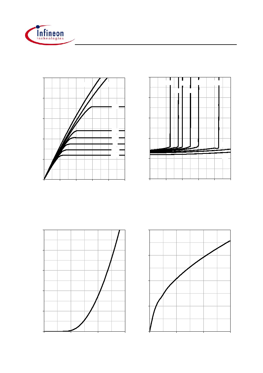
5 Typ. output characteristics
6 Typ. drain-source on resistance
I
D
=f(V
DS
); T
j
=25 °C
R
DS(on)
=f(I
D
); T
j
=25 °C
parameter: V
GS
parameter: V
GS
7 Typ. transfer characteristics
8 Typ. forward transconductance
I
D
=f(V
GS
); |V
DS
|>2|I
D
|R
DS(on)max
g
fs
=f(I
D
); T
j
=25 °C
-0.2 V
-0.1 V
0 V
0.1 V
0.2 V
0.5 V
1 V
10 V
0
20
40
60
80
100
0
0.04
0.08
0.12
0.16
0.2
I
D
[A]
R
D
S
(on)
[
]
0
0.05
0.1
0.15
0.2
0.25
-2
-1
0
1
V
GS
[V]
I
D
[A]
0
0.05
0.1
0.15
0.2
0.0
0.0
0.1
0.1
I
D
[A]
g
fs
[S]
-0.2 V
-0.1 V
0 V
0.1 V
0.2 V
0.5 V
1 V
10 V
0
0.05
0.1
0.15
0.2
0.25
0
2
4
6
8
10
V
DS
[V]
I
D
[A]
Rev. 1.0
page 5
2003-04-03