2002-07-17
Page 1
Preliminary data
BSO301SP
OptiMOS
-P Small-Signal-Transistor
Product Summary
V
DS
-30
V
R
DS(on)
8
m
I
D
-14.9
A
Feature
·
P-Channel
·
Enhancement mode
·
Logic Level
·
150°C operating temperature
·
Avalanche rated
·
dv/dt rated
·
Ideal for fast switching buck converter
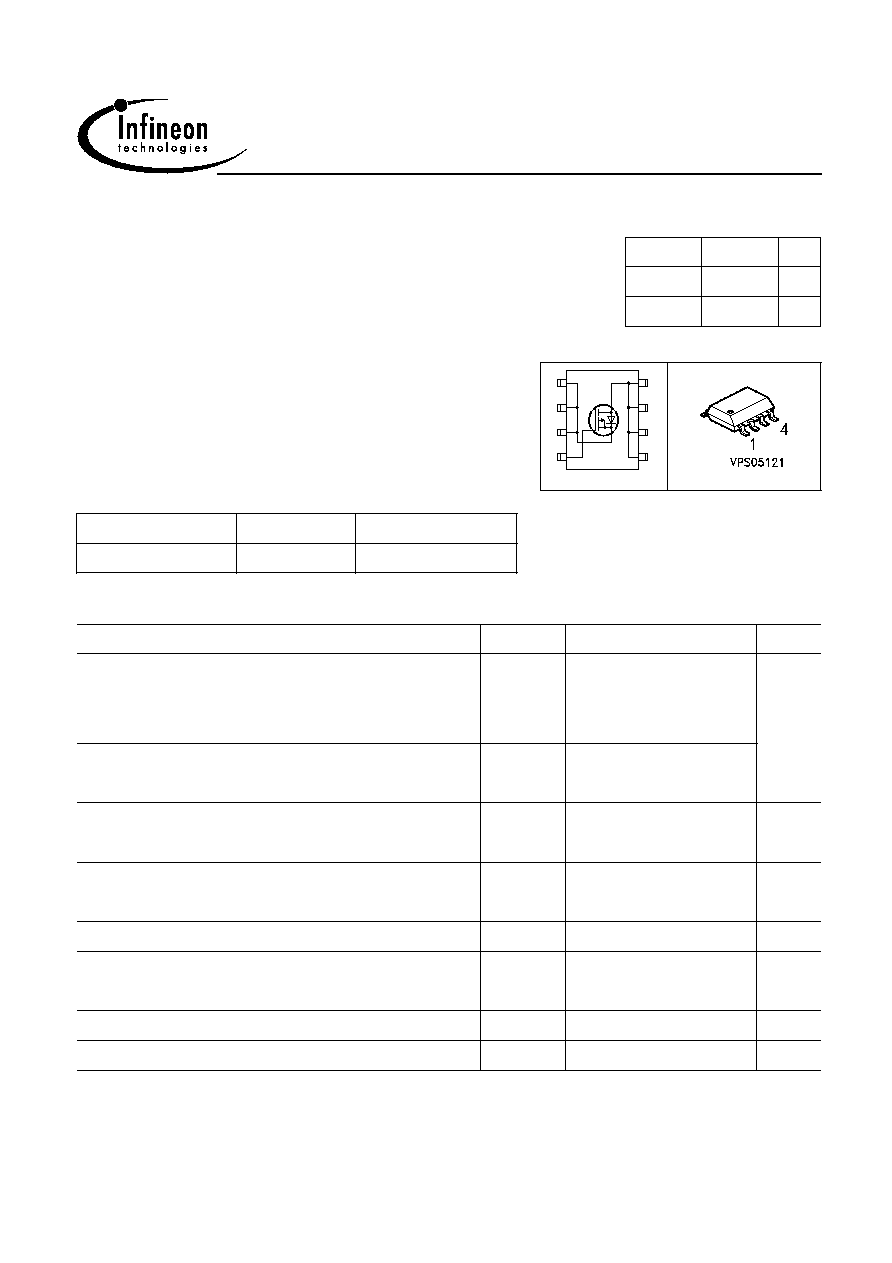
SIS00062
G
4
5
D
S
3
6
D
S
2
7
D
S
1
8
Top View
D
Type
Package
Ordering Code
BSO301SP
SO 8
Q67042-S4086
Maximum Ratings, at T
j
= 25 °C, unless otherwise specified
Parameter
Symbol
Value
Unit
Continuous drain current
T
A
=25°C
T
A
=70°C
I
D
-14.9
-11.9
A
Pulsed drain current
T
A
=25°C
I
D puls
-59.6
Avalanche energy, single pulse
I
D
=-14.9 A , V
DD
=-25V, R
GS
=25
E
AS
248
mJ
Reverse diode dv/dt
I
S
=-14.9A, V
DS
=-24V, di/dt=200A/µs, T
jmax
=150°C
dv/dt
-6
kV/µs
Gate source voltage
V
GS
±20
V
Power dissipation
T
A
=25°C
P
tot
2.5
W
Operating and storage temperature
T
j ,
T
stg
-55... +150
°C
IEC climatic category; DIN IEC 68-1
55/150/56

2002-07-17
Page 2
Preliminary data
BSO301SP
Thermal Characteristics
Parameter
Symbol
Values
Unit
min.
typ.
max.
Characteristics
Thermal resistance, junction - soldering point
R
thJS
-
-
35
K/W
SMD version, device on PCB:
@ min. footprint, t < 10s
@ 6 cm
2
cooling area
1)
R
thJA
-
-
-
-
110
50
Electrical Characteristics, at T
j
= 25 °C, unless otherwise specified
Parameter
Symbol
Values
Unit
min.
typ.
max.
Static Characteristics
Drain-source breakdown voltage
V
GS
=0, I
D
=-250µA
V
(BR)DSS
-30
-
-
V
Gate threshold voltage, V
GS
= V
DS
I
D
=-250µA
V
GS(th)
-1
-1.5
-2
Zero gate voltage drain current
V
DS
=-30V, V
GS
=0, T
j
=25°C
V
DS
=-30V, V
GS
=0, T
j
=150°C
I
DSS
-
-
-0.1
-10
-1
-100
µA
Gate-source leakage current
V
GS
=-20V, V
DS
=0
I
GSS
-
-10
-100 nA
Drain-source on-state resistance
V
GS
=-4.5V, I
D
=-12.1A
R
DS(on)
-
9.1
12
m
Drain-source on-state resistance
V
GS
=-10V, I
D
=-14.9A
R
DS(on)
-
6.3
8
1Device on 40mm*40mm*1.5mm epoxy PCB FR4 with 6cm2 (one layer, 70 µm thick) copper area for drain
connection. PCB is vertical without blown air; t
10 sec.
2002-07-17
Page 3
Preliminary data
BSO301SP
Electrical Characteristics, at T
j
= 25 °C, unless otherwise specified
Parameter
Symbol
Conditions
Values
Unit
min.
typ.
max.
Dynamic Characteristics
Transconductance
g
fs
ç
V
DS
ç
2*
ç
I
D
ç
*R
DS(on)max
,
I
D
=-11.9A
22
44
-
S
Input capacitance
C
iss
V
GS
=0, V
DS
=-25V,
f=1MHz
-
4510
-
pF
Output capacitance
C
oss
-
1140
-
Reverse transfer capacitance
C
rss
-
950
-
Turn-on delay time
t
d(on)
V
DD
=-15V, V
GS
=-10V,
I
D
=-1A, R
G
=6
-
17
25
ns
Rise time
t
r
-
26
38
Turn-off delay time
t
d(off)
-
161
240
Fall time
t
f
-
120
180
Gate Charge Characteristics
Gate to source charge
Q
gs
V
DD
=-24V, I
D
=-14.9A
-
-11
-16
nC
Gate to drain charge
Q
gd
-
-40
-61
Gate charge total
Q
g
V
DD
=-24V, I
D
=-14.9A,
V
GS
=0 to -10V
-
-121
-181
Gate plateau voltage
V
(plateau) V
DD
=-24V, I
D
=-14.9A
-
-2.4
-
V
Reverse Diode
Inverse diode continuous
forward current
I
S
T
A
=25°C
-
-
-3.3
A
Inv. diode direct current, pulsed I
SM
-
-
-59.6
Inverse diode forward voltage V
SD
V
GS
=0, |IF| = |ID|
-
-0.75
-1.2
V
Reverse recovery time
t
rr
V
R
=-15V, |I
F
|
=
|l
D
|,
di
F
/dt=100A/µs
-
36
45
ns
Reverse recovery charge
Q
rr
-
27
34
nC

2002-07-17
Page 4
Preliminary data
BSO301SP
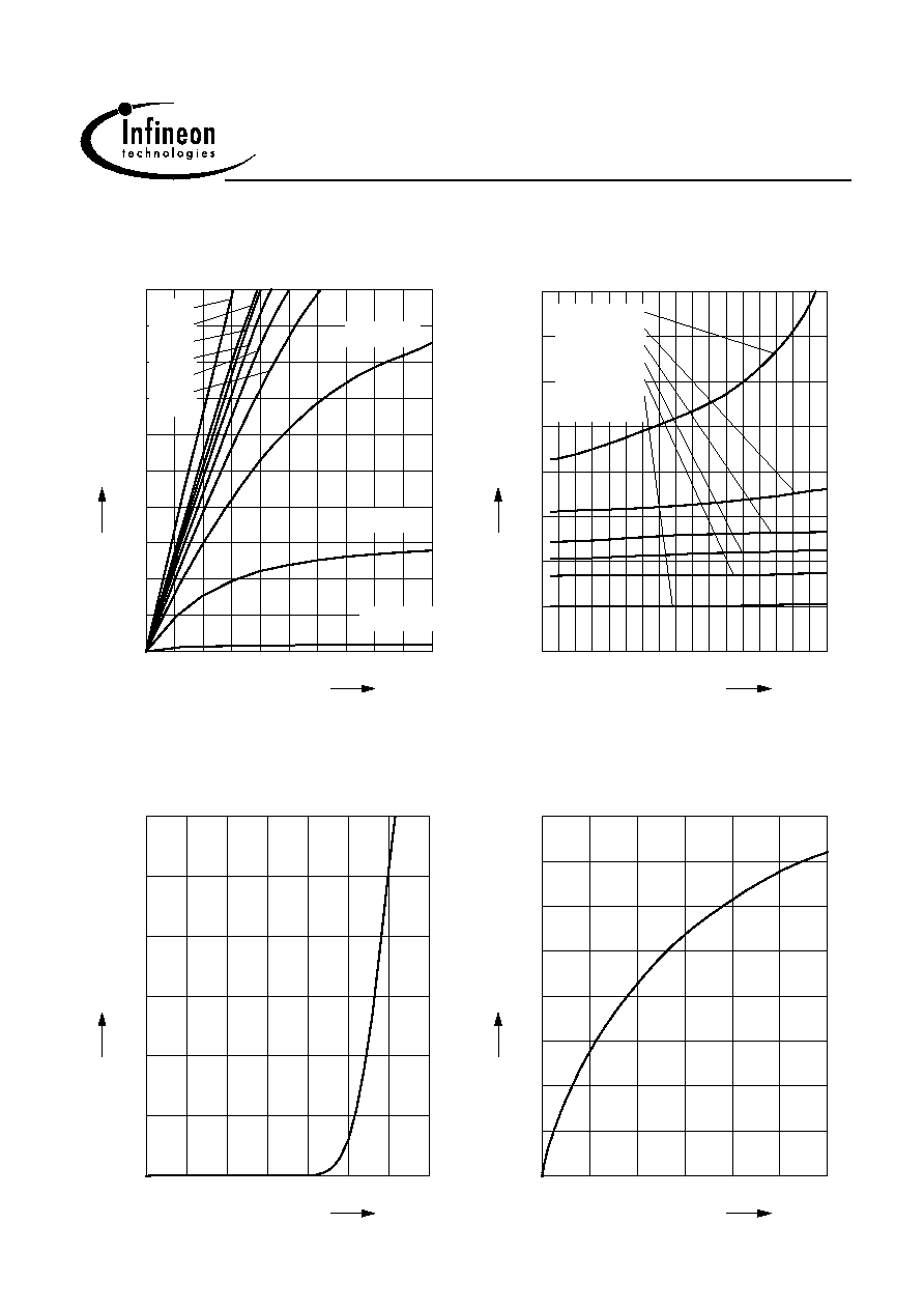
1 Power dissipation
P
tot
= f (T
A
)
0
20
40
60
80
100
120
°C
160
T
A
0
0.4
0.8
1.2
1.6
2
2.4
W
3.2
BSO301SP
P
tot
2 Drain current
I
D
= f (T
A
)
parameter: |V
GS
|
10 V
0
20
40
60
80
100
120
°C
160
T
A
0
-2
-4
-6
-8
-10
-12
A
-16
BSO301SP
I
D
3 Safe operating area
I
D
= f ( V
DS
)
parameter : D = 0 , T
A
= 25 °C
-10
-1
-10
0
-10
1
-10
2
V
V
DS
-2
-10
-1
-10
0
-10
1
-10
2
-10
A
BSO301SP
I
D
R
DS
(o
n)
=
DC
10 ms
1 ms
tp = 290.0µs
4 Transient thermal impedance
Z
thJS
= f (t
p
)
parameter : D = t
p
/T
10
-7
10
-6
10
-5
10
-4
10
-3
10
-2
10
0
s
t
p
-5
10
-4
10
-3
10
-2
10
-1
10
0
10
1
10
2
10
K/W
BSO301SP
Z
thJS
single pulse
0.01
0.02
0.05
0.10
0.20
D = 0.50
2002-07-17
Page 5
Preliminary data
BSO301SP
5 Typ. output characteristic
I
D
= f (V
DS
)
parameter: Tj =25°C
0
0.1 0.2 0.3 0.4 0.5 0.6 0.7 0.8
V
1
- V
DS
0
5
10
15
20
25
30
35
40
A
50
-
I
D
Vgs= -2.5V
Vgs= -3V
Vgs= -3.5V
-10V
-6V
-5.5V
-5V
-4.5V
-4V
6 Typ. drain-source on resistance
R
DS(on)
= f (I
D
)
parameter: V
GS
6
10
14
18
22
26
30
34
A
40
- I
D
4
6
8
10
12
14
16
m
20
R
DS
(
on)
Vgs = - 3,5V
Vgs = - 4V
Vgs = - 4.5V
Vgs= - 5V
Vgs = - 6V
Vgs = - 10V
7 Typ. transfer characteristics
I
D
= f ( V
GS
); |V
DS
|
2 x |I
D
| x R
DS(on)max
parameter: T
j
= 25 °C
0
-0.5
-1
-1.5
-2
-2.5
V
-3.5
V
GS
0
-5
-10
-15
-20
A
-30
I
D
8 Typ. forward transconductance
g
fs
= f(I
D
)
parameter: Tj = 25 °C
0
-5
-10
-15
-20
A
-30
I
D
0
10
20
30
40
50
60
S
80
g
fs