
1999-09-22
Page 1
Preliminary data
BSO 215 C
SIPMOS
Û
Small-Signal-Transistor
Product Summary
N
P
Drain source voltage
V
DS
20
-20
V
Drain-Source on-state
resistance
R
DS(on)
0.1
0.1
Continuous drain current
I
D
3.7
-3.7
A
Features
ñ
Dual N- and P -Channel
ñ
Enhancement mode
ñ
Logic Level
ñ
Avalanche rated
ñ
d
v/dt rated
Type
Package
Ordering Code
BSO 215 C
SO 8
Q67041-S4025
Maximum Ratings,at
T
j
= 25 ¯C, unless otherwise specified
Parameter
Symbol
Value
Unit
N
P
Continuous drain current
T
A
= 25 ¯C
T
A
= 70 ¯C
I
D
3.7
3
-3.7
-3
A
Pulsed drain current
T
A
= 25 ¯C
I
D puls
14.8
-14.8
Avalanche energy, single pulse
I
D
= 3 A,
V
DD
= 15 V,
R
GS
= 25
I
D
= -3.7 A ,
V
DD
= -15 V,
R
GS
= 25
E
AS
26
-
-
68
mJ
Avalanche energy, periodic limited by
T
jmax
E
AR
0.2
0.2
Reverse diode d
v/dt, T
jmax
= 150 ¯C
I
S
= 3 A,
V
DS
= 16 V, d
i/dt = 200 A/çs
I
S
= -2.7 A,
V
DS
= -16 V, d
i/dt = -200 A/çs
d
v/dt
6
-
-
6
kV/çs
Gate source voltage
V
GS
Ý20
Ý20
V
Power dissipation
T
A
= 25 ¯C
P
tot
2
2
W
Operating and storage temperature
T
j ,
T
stg
-55...+150
¯C
IEC climatic category; DIN IEC 68-1
55/150/56

1999-09-22
Page 2
Preliminary data
BSO 215 C
Termal Characteristics
Parameter
Symbol
Values
Unit
min.
typ.
max.
Dynamic Characteristics
Thermal resistance, junction - soldering point
N
P
R
thJS
-
-
-
-
40
40
K/W
SMD version, device on PCB:
@ min. footprint; t
10 sec.
@ 6 cm
2
cooling area
1)
; t
10 sec.
@ min. footprint; t
10 sec.
@ 6 cm
2
cooling area
1)
; t
10 sec.
N
N
P
P
R
thJA
-
-
-
-
-
-
-
-
110
62.5
100
62.5
Static Characteristics, at
T
j
= 25 ¯C, unless otherwise specified
Drain- source breakdown voltage
V
GS
= 0 V,
I
D
= 250 çA
V
GS
= 0 V,
I
D
= -250 çA
N
P
V
(BR)DSS
20
-20
-
-
-
-
V
Gate threshold voltage,
V
GS
=
V
DS
I
D
= 10 çA
I
D
= -450 çA
N
P
V
GS(th)
1.2
-1
1.5
-1.5
2
-2
Zero gate voltage drain current
V
DS
= 20 V,
V
GS
= 0 V,
T
j
= 25 ¯C
V
DS
= 20 V,
V
GS
= 0 V,
T
j
= 125 ¯C
V
DS
= -20 V,
V
GS
= 0 V,
T
j
= 25 ¯C
V
DS
= -20 V,
V
GS
= 0 V,
T
j
= 125 ¯C
N
N
P
P
I
DSS
-
-
-
-
0.1
10
-0.1
-10
1
100
-1
-100
çA
Gate-source leakage current
V
GS
= 20 V,
V
DS
= 0 V
V
GS
= -20 V,
V
DS
= 0 V
N
P
I
GSS
-
-
10
-10
100
-100
nA
Drain-Source on-state resistance
V
GS
= 4.5 V,
I
D
= 3 A
V
GS
= -4.5 V,
I
D
= -3 A
N
P
R
DS(on)
-
-
0.1
0.1
0.15
0.15
Drain-Source on-state resistance
V
GS
= 10 V,
I
D
= 3.7 A
V
GS
= -10 V ,
I
D
= -3.7 A
N
P
R
DS(on)
-
-
0.05
0.06
0.1
0.1
1Device on 40mm*40mm*1.5mm epoxy PCB FR4 with 6cm 2 (one layer, 70 çm thick) copper area for drain
connection. PCB is vertical without blown air.

1999-09-22
Page 3
Preliminary data
BSO 215 C
Electrical Characteristics, at
T
j
= 25 ¯C, unless otherwise specified
Parameter
Symbol
Values
Unit
min.
typ.
max.
Characteristics
Transconductance
V
DS
2
*
I
D *
R
DS(on)max
,
I
D
= 3 A
VV
DS
2
*
I
D *
R
DS(on)max
,
I
D
= -3 A
N
P
g
fs
2.1
2.6
4.4
5.2
-
-
S
Input capacitance
V
GS
= 0 V,
V
DS
= 25 V,
f = 1 MHz
V
GS
= 0 V,
V
DS
= -25 V,
f = 1 MHz
N
P
C
iss
-
-
197
380
246
475
pF
Output capacitance
V
GS
= 0 V,
V
DS
= 25 V,
f = 1 MHz
V
GS
= 0 V,
V
DS
= -25 V,
f = 1 MHz
N
P
C
oss
-
-
109
290
136
360
Reverse transfer capacitance
V
GS
= 0 V,
V
DS
= 25 V,
f = 1 MHz
V
GS
= 0 V,
V
DS
= -25 V,
f = 1 MHz
N
P
C
rss
-
-
59
103
74
128
Turn-on delay time
V
DD
= 10 V,
V
GS
= 4.5 V,
I
D
= 3 A,
R
G
= 33
V
DD
= -10 ,
V
GS
= -4.5 V,
I
D
= -3 A,
R
G
= 13
N
P
t
d(on)
-
-
15
24
22.5
36
ns
Rise time
V
DD
= 10 V,
V
GS
= 4.5 V,
I
D
= 3 A,
R
G
= 33
V
DD
= -10 ,
V
GS
= -4.5 V,
I
D
= -3 A,
R
G
= 13
N
P
t
r
-
-
88
236
132
354
Turn-off delay time
V
DD
= 10 V,
V
GS
= 4.5 V,
I
D
= 3 A,
R
G
= 33
V
DD
= -10 ,
V
GS
= -4.5 V,
I
D
= -3 A,
R
G
= 13
N
P
t
d(off)
-
-
12.3
87
18.5
130
Fall time
V
DD
= 10 V,
V
GS
= 4.5 V,
I
D
= 3 A,
R
G
= 33
V
DD
= -10 V,
V
GS
= -4.5 V,
I
D
= -3 A,
R
G
= 13
N
P
t
f
-
-
17.1
168
25.7
252

1999-09-22
Page 4
Preliminary data
BSO 215 C
Electrical Characteristics, at
T
j
= 25 ¯C, unless otherwise specified
Parameter
Symbol
Values
Unit
min.
typ.
max.
Characteristics
Gate to source charge
V
DD
= 16 ,
I
D
= 3.7 A
V
DD
= -16 ,
I
D
= -3.7 A
N
P
Q
gs
-
-
1.3
1.9
2
2.9
nC
Gate to drain charge
V
DD
= 16 ,
I
D
= 3.7 A
V
DD
= -16 ,
I
D
= -3.7 A
N
P
Q
gd
-
-
3
4.4
4.5
6.6
Gate charge total
V
DD
= 16 ,
I
D
= 3.7 A,
V
GS
= 0 to 10V
V
DD
= -16 ,
I
D
= -3.7 A,
V
GS
= 0 to -10V
N
P
Q
g
-
-
7.7
13.2
11.5
19.8
Gate plateau voltage
V
DD
= 16 ,
I
D
= 3.7 A
V
DD
= -16 ,
I
D
= -3.7 A
N
P
V
(plateau)
-
-
3.5
2.8
-
-
V
Reverse Diode
Inverse diode continuous forward current
T
A
= 25 ¯C
N
P
I
S
-
-
-
-
3.7
-3.7
A
Inverse diode direct current,pulsed
T
A
= 25 ¯C
N
P
I
SM
-
-
-
-
14.8
-14.8
Inverse diode forward voltage
V
GS
= 0 V,
I
F
=
I
S
V
GS
= 0 V,
I
F
=
I
S
N
P
V
SD
-
-
0.84
-0.82
1.1
-1
V
Reverse recovery time
V
R
= 10 V,
I
F=
l
S
, d
i
F
/d
t = 100 A/çs
V
R
= -10 V,
I
F=
l
S
, d
i
F
/d
t = -100 A/çs
N
P
t
rr
-
-
46.5
137
70
205
ns
Reverse recovery charge
V
R
= 10 V,
I
F=
l
S
, d
i
F
/d
t = 100 A/çs
V
R
= -10 V,
I
F=
l
S
, d
i
F
/d
t = -100 A/çs
N
P
Q
rr
-
-
18.4
80
27.6
120
çC

1999-09-22
Page 5
Preliminary data
BSO 215 C
Power Dissipation (P-Ch.)
P
tot
=
f (T
A
)
0
20
40
60
80
100
120
¯C
160
T
A
0.0
0.2
0.4
0.6
0.8
1.0
1.2
1.4
1.6
1.8
W
2.2
BSO 215 C
P
tot
Power Dissipation (N-Ch.)
P
tot
=
f (T
A
)
0
20
40
60
80
100
120
¯C
160
T
A
0.0
0.2
0.4
0.6
0.8
1.0
1.2
1.4
1.6
1.8
W
2.2
BSO 215 C
P
tot
Drain current (N-Ch.)
I
D
=
f (T
A
)
parameter:
V
GS
10 V
0
20
40
60
80
100
120
¯C
160
T
A
0.0
0.4
0.8
1.2
1.6
2.0
2.4
2.8
3.2
A
4.0
BSO 215 C
I
D
Drain current (P-Ch.)
I
D
=
f (T
A
)
parameter:
V
GS
-10 V
0
20
40
60
80
100
120
¯C
160
T
A
0.0
-0.4
-0.8
-1.2
-1.6
-2.0
-2.4
-2.8
-3.2
A
-4.0
BSO 215 C
I
D
1999-09-22
Page 6
Preliminary data
BSO 215 C
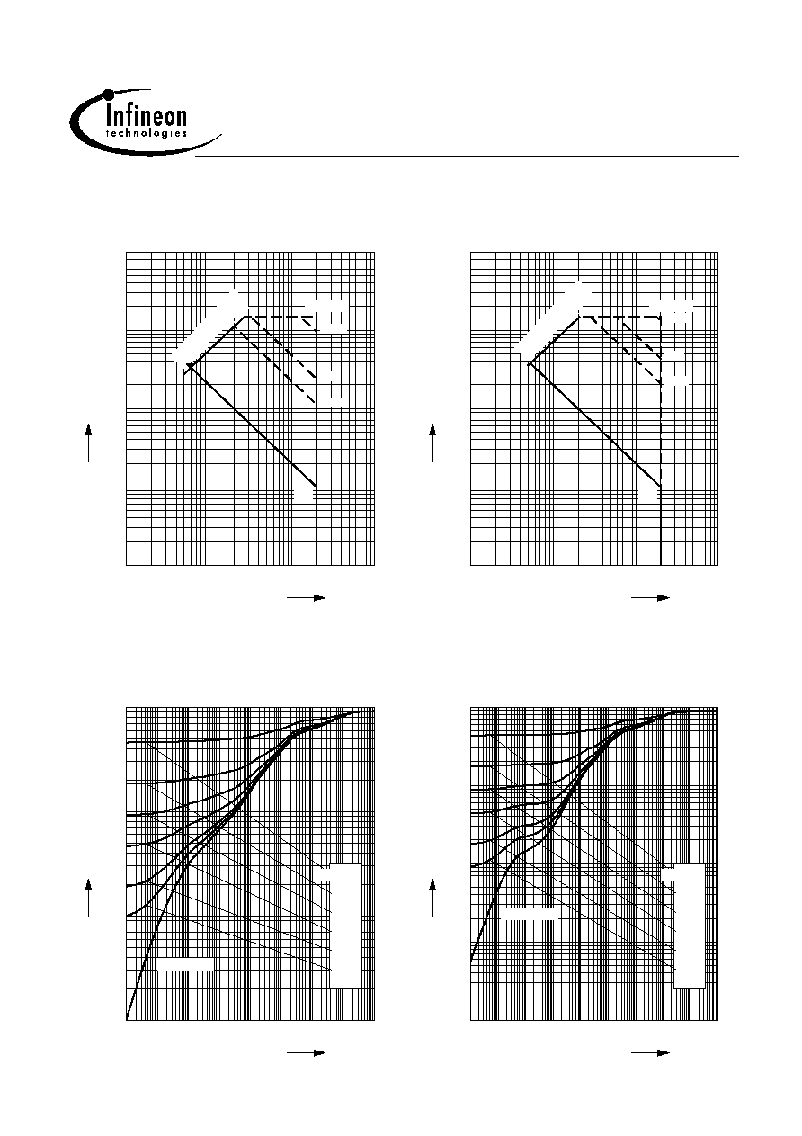
Safe operating area (N-Ch.)
I
D
=
f ( V
DS
)
parameter :
D = 0 , T
A
= 25 ¯C
10
-1
10
0
10
1
10
2
V
V
DS
-2
10
-1
10
0
10
1
10
2
10
A
BSO 215 C
I
D
R
D
S
(on)
=
V
D
S
/
I
D
DC
10 ms
1 ms
100 çs
t
p = 57.0çs
Safe operating area (P-Ch.)
I
D
=
f ( V
DS
)
parameter :
D = 0 , T
A
= 25 ¯C
-10
-1
-10
0
-10
1
-10
2
V
V
DS
-2
-10
-1
-10
0
-10
1
-10
2
-10
A
BSO 215 C
I
D
R
D
S(
on)
=
V
D
S
/
I
D
DC
10 ms
1 ms
100 çs
t
p = 86.0çs
Transient thermal impedance (N-Ch.)
Z
thJC
=
f(t
p
)
parameter :
D = t
p
/
T
10
-5
10
-4
10
-3
10
-2
10
-1
10
0
10
1
10
3
s
t
p
-1
10
0
10
1
10
2
10
K/W
BSO 215 C
Z
thJC
single pulse
0.01
0.02
0.05
0.10
0.20
D = 0.50
Transient thermal impedance (P-Ch.)
Z
thJC
=
f(t
p
)
parameter :
D = t
p
/
T
10
-5
10
-4
10
-3
10
-2
10
-1
10
0
10
1
10
2
10
4
s
t
p
-2
10
-1
10
0
10
1
10
2
10
K/W
BSO 215 C
Z
thJC
single pulse
0.01
0.02
0.05
0.10
0.20
D = 0.50

1999-09-22
Page 7
Preliminary data
BSO 215 C
Typ. output characteristics (N-Ch.)
I
D
=
f (V
DS
)
parameter:
t
p
= 80 çs
0.0
0.5 1.0
1.5 2.0
2.5 3.0
3.5 4.0
V
5.0
V
DS
0
1
2
3
4
5
6
7
8
A
10
BSO 215 C
I
D
V
GS [V]
a
a
2.5
b
b
2.7
c
c
3.0
d
d
3.2
e
e
3.5
f
f
3.7
g
g
4.0
h
h
4.2
i
i
4.5
j
P
tot
= 2.00W
j
5.0
Typ. output characteristics (P-Ch.)
I
D
=
f (V
DS
)
parameter:
t
p
= 80 çs
0.0 -0.5 -1.0 -1.5 -2.0 -2.5 -3.0 -3.5 -4.0 V
-5.0
V
DS
0
-1
-2
-3
-4
-5
-6
-7
-8
A
-10
BSO 215 C
I
D
V
GS [V]
a
a
-2.5
b
b
-2.7
c
c
-3.0
d
d
-3.2
e
e
-3.5
f
f
-3.7
g
P
tot
= 2.00W
g
-4.0
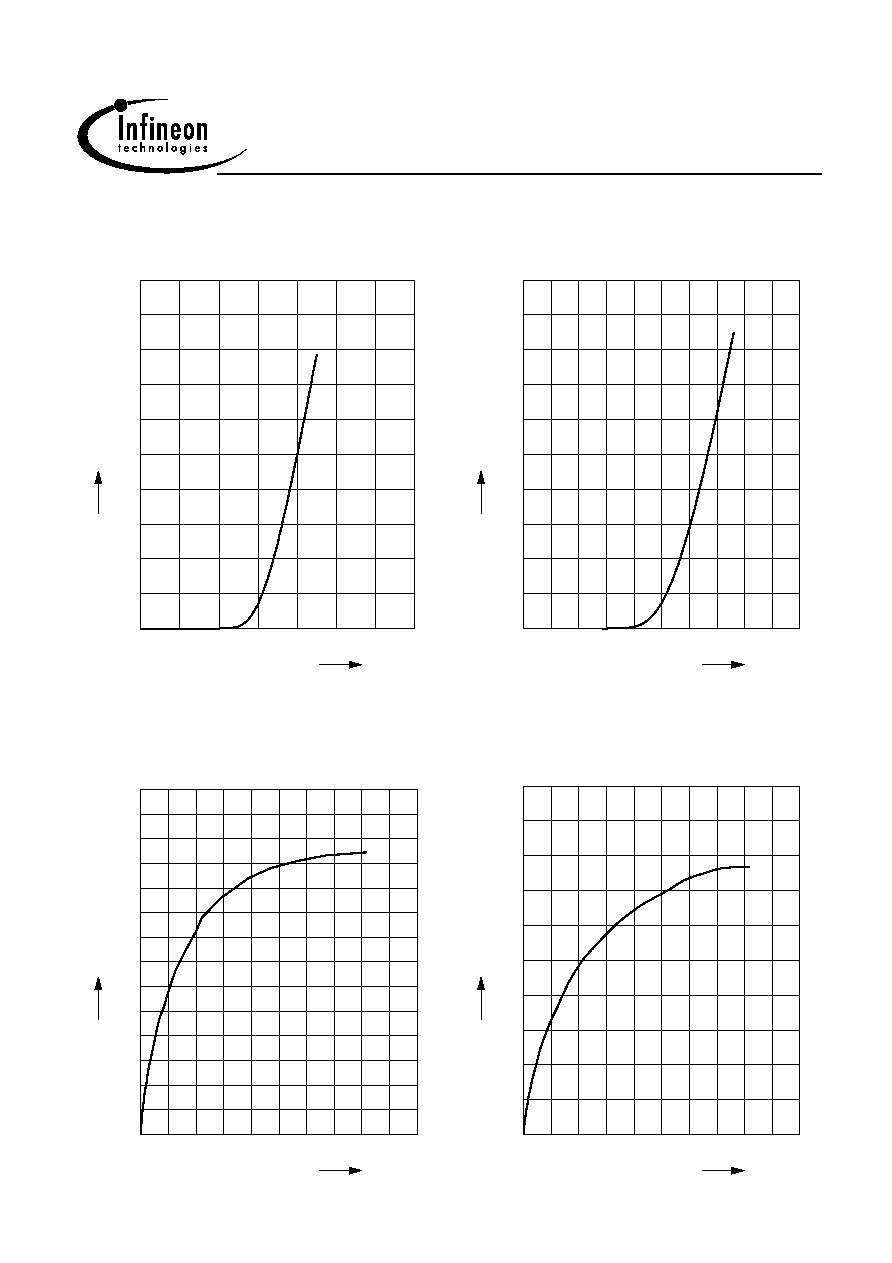
Typ. drain-source-on-resistance (N-Ch.)
R
DS(on)
=
f (I
D
)
parameter:
V
GS
0.0
1.0
2.0
3.0
4.0
5.0
A
7.0
I
D
0.00
0.04
0.08
0.12
0.16
0.20
0.24
0.32
BSO 215 C
R
DS(on)
d
V
GS
[V] =
d
3.2
e
e
3.5
f
f
3.7
g
g
4.0
h
h
4.2
i
i
4.5
j
j
5.0
Typ. drain-source-on-resistance (P-Ch.)
R
DS(on)
=
f (I
D
)
parameter:
V
GS
0.0
-1.0
-2.0
-3.0
-4.0
-5.0
¯C
-7.0
T
j
0.00
0.04
0.08
0.12
0.16
0.20
0.24
0.32
BSO 215 C
R
DS(on)
b
V
GS
[V] =
b
-2.7
c
c
-3.0
d
d
-3.2
e
e
-3.5
f
f
-3.7
g
g
-4.0
1999-09-22
Page 8
Preliminary data
BSO 215 C
Typ. transfer characteristics (N-Ch.)
parameter:
t
p
= 80 çs
I
D
=
f (V
GS
),
V
DS
2 x
I
D
x
R
DS(on)max
0
1
2
3
4
5
V
GS
7
V
0
1
2
3
4
5
6
7
8
A
10
I
D
Typ. transfer characteristics (P-Ch.)
parameter:
t
p
= 80 çs
I
D
=
f (V
GS
),
V
DS
2 x
I
D
x
R
DS(on)max
0.0 -0.5 -1.0 -1.5 -2.0 -2.5 -3.0 -3.5 -4.0 V
-5.0
V
GS
0
-1
-2
-3
-4
-5
-6
-7
-8
A
-10
I
D
Typ. forward transconductance (N-Ch.)
g
fs
= f(
I
D
);
T
j
= 25 ¯C
parameter:
g
fs
0
1
2
3
4
5
6
7
8
A
10
I
D
0.0
0.5
1.0
1.5
2.0
2.5
3.0
3.5
4.0
4.5
5.0
5.5
6.0
S
7.0
g
fs
Typ. forward transconductance (P-Ch.)
g
fs
= f(
I
D
);
T
j
= 25 ¯C
parameter:
g
fs
0
-1
-2
-3
-4
-5
-6
-7
-8
A
-10
I
D
0
1
2
3
4
5
6
7
8
S
10
g
fs

1999-09-22
Page 9
Preliminary data
BSO 215 C
Drain-source on-resistance (N-Ch.)
R
DS(on)
= f (
T
j
)
parameter :
I
D
= 3.7 A ,
V
GS
= 10 V
-60
-20
20
60
100
¯C
180
T
j
0.00
0.02
0.04
0.06
0.08
0.10
0.12
0.14
0.16
0.18
0.20
0.22
0.26
BSO 215 C
R
DS(on)
typ
98%
Drain-source on-resistance (P-Ch.)
R
DS(on)
= f
(T
j
)
parameter :
I
D
= -3.7 A ,
V
GS
= -10 V
-60
-20
20
60
100
¯C
180
T
j
0.00
0.02
0.04
0.06
0.08
0.10
0.12
0.14
0.16
0.19
BSO 215 C
R
DS(on)
typ
98%
Gate threshold voltage (N-Ch.)
V
GS(th)
=
f (Tj)
parameter:
V
GS
=
V
DS
,
I
D
= 10 çA
-60
-20
20
60
100
¯C
160
T
j
0.0
0.2
0.5
0.8
1.0
1.2
1.5
1.8
2.0
2.2
2.5
V
3.0
V
GS(th)
2%
-60
-20
20
60
100
¯C
160
T
j
0.0
0.2
0.5
0.8
1.0
1.2
1.5
1.8
2.0
2.2
2.5
V
3.0
V
GS(th)
typ
-60
-20
20
60
100
¯C
160
T
j
0.0
0.2
0.5
0.8
1.0
1.2
1.5
1.8
2.0
2.2
2.5
V
3.0
V
GS(th)
98%
-60
-20
20
60
100
¯C
160
T
j
0.0
0.2
0.5
0.8
1.0
1.2
1.5
1.8
2.0
2.2
2.5
V
3.0
V
GS(th)
Gate threshold voltage (P-Ch.)
V
GS(th)
=
f (Tj)
parameter:
V
GS
=
V
DS
,
I
D
= -450 çA
-60
-20
20
60
100
¯C
160
T
j
0.0
-0.5
-1.0
-1.5
-2.0
V
-3.0
V
GS(th)
2%
-60
-20
20
60
100
¯C
160
T
j
0.0
-0.5
-1.0
-1.5
-2.0
V
-3.0
V
GS(th)
typ
-60
-20
20
60
100
¯C
160
T
j
0.0
-0.5
-1.0
-1.5
-2.0
V
-3.0
V
GS(th)
98%
-60
-20
20
60
100
¯C
160
T
j
0.0
-0.5
-1.0
-1.5
-2.0
V
-3.0
V
GS(th)

1999-09-22
Page 10
Preliminary data
BSO 215 C
Typ. capacitances (N-Ch.)
C = f(V
DS
)
parameter:
V
GS
=0 V,
f=1 MHz
0
5
10
15
V
25
V
DS
1
10
2
10
3
10
pF
C
C
iss
C
oss
C
rss
Typ. capacitances (P-Ch.)
C = f(V
DS
)
parameter:
V
GS
=0 V,
f=1 MHz
0
-5
-10
-15
V
-25
V
DS
1
10
2
10
3
10
4
10
pF
C
C
oss
0
-5
-10
-15
V
-25
V
DS
1
10
2
10
3
10
4
10
pF
C
C
iss
C
rss
Forward characteristics of reverse diode
I
F
=
f (V
SD
), (N-Ch.)
parameter:
Tj , t
p
= 80 çs
0.0
0.4
0.8
1.2
1.6
2.0
2.4
V
3.0
V
SD
-2
10
-1
10
0
10
1
10
A
BSO 215 C
I
F
T
j
= 25 ¯C typ
T
j
= 25 ¯C (98%)
T
j
= 150 ¯C typ
T
j
= 150 ¯C (98%)
Forward characteristics of reverse diode
I
F
=
f (V
SD
), (P-Ch.)
parameter:
T
j
,
t
p
= 80 çs
0.0
-0.4
-0.8
-1.2
-1.6
-2.0
-2.4 V
-3.0
V
SD
-2
-10
-1
-10
0
-10
1
-10
A
BSO 215 C
I
F
T
j
= 25 ¯C typ
T
j
= 25 ¯C (98%)
T
j
= 150 ¯C typ
T
j
= 150 ¯C (98%)

1999-09-22
Page 11
Preliminary data
BSO 215 C
Avalanche Energy
E
AS
=
f (T
j
) (N-Ch.)
parameter:
I
D
= 3 A,
V
DD
= 15 V
R
GS
= 25
25
45
65
85
105
125
¯C
165
T
j
0
5
10
15
20
mJ
30
E
AS
Avalanche Energy
E
AS
=
f (T
j
)
parameter:
I
D
= -3.7 A ,
V
DD
= -15 V
R
GS
= 25
25
45
65
85
105
125
¯C
165
T
j
0
10
20
30
40
50
mJ
70
E
AS
Typ. gate charge (N-Ch.)
V
GS
= f
(Q
Gate
)
parameter:
I
D
= 3.7 A
0
2
4
6
8
nC
12
Q
Gate
0
2
4
6
8
10
12
V
16
BSO 215 C
V
GS
DS max
V
0,8
DS max
V
0,2
Typ. gate charge (P-Ch.)
V
GS
= f
(Q
Gate
)
parameter:
I
D
= -3.7 A
0
2
4
6
8
10
12
14
16 nC
19
Q
Gate
0
-2
-4
-6
-8
-10
-12
V
-16
BSO 215 C
V
GS
DS max
V
0,8
DS max
V
0,2

1999-09-22
Page 12
Preliminary data
BSO 215 C
Drain-source breakdown voltage
V
(BR)DSS
= f
(T
j
), (N-Ch.)
-60
-20
20
60
100
¯C
180
T
j
18.0
18.5
19.0
19.5
20.0
20.5
21.0
21.5
22.0
22.5
23.0
23.5
V
24.5
BSO 215 C
V
(BR)DSS
Drain-source breakdown voltage
V
(BR)DSS
= f
(T
j
)
-60
-20
20
60
100
¯C
180
T
j
-18.0
-18.5
-19.0
-19.5
-20.0
-20.5
-21.0
-21.5
-22.0
-22.5
-23.0
-23.5
V
-24.5
BSO 215 C
V
(BR)DSS

1999-09-22
Page 13
Preliminary data
BSO 215 C
Published by
Infineon Technologies AG,
Bereichs Kommunikation
St.-Martin-Strasse 53,
D-81541 M■nchen
ˋ Infineon Technologies AG 1999
All Rights Reserved.
Attention please!
The information herein is given to describe certain components and shall not be considered as warranted
characteristics.
Terms of delivery and rights to technical change reserved.
We hereby disclaim any and all warranties, including but not limited to warranties of non-infringement,
regarding circuits, descriptions and charts stated herein.
Infineon Technologies is an approved CECC manufacturer.
Information
For further information on technology, delivery terms and conditions and prices please contact your nearest
Infineon Technologies Office in Germany or our Infineon Technologies Reprensatives worldwide (see address list).
Warnings
Due to technical requirements components may contain dangerous substances.
For information on the types in question please contact your nearest Infineon Technologies Office.
Infineon Technologies Components may only be used in life-support devices or systems with the express
written approval of Infineon Technologies, if a failure of such components can reasonably be expected to
cause the failure of that life-support device or system, or to affect the safety or effectiveness of that device
or system Life support devices or systems are intended to be implanted in the human body, or to support
and/or maintain and sustain and/or protect human life. If they fail, it is reasonable to assume that the health
of the user or other persons may be endangered.