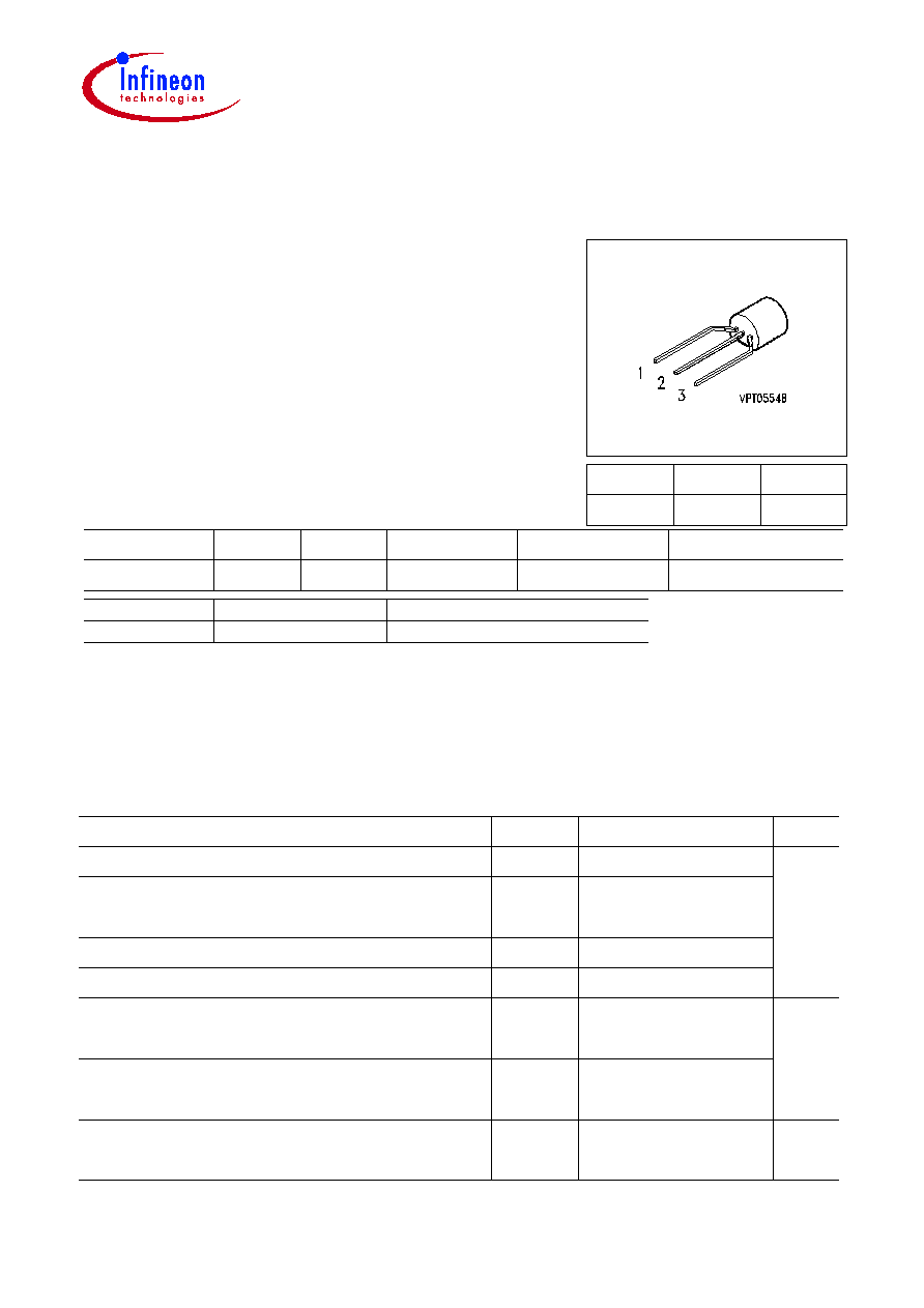
BS 107
Data Sheet
2
05.99
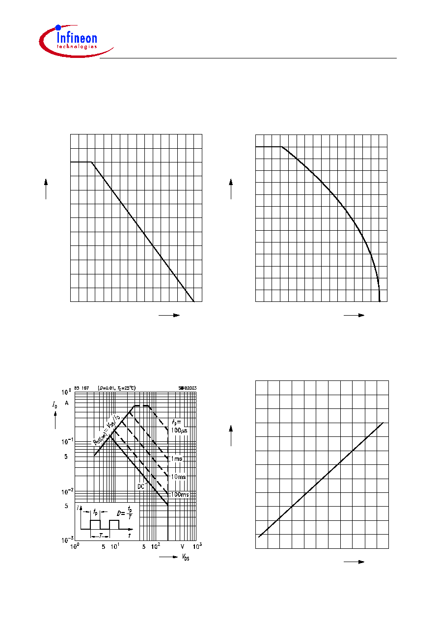
Maximum Ratings
Parameter
Symbol
Values
Unit
Chip or operating temperature
T
j
-55 ... + 150
°C
Storage temperature
T
stg
-55 ... + 150
Thermal resistance, chip to ambient air
1)
R
thJA
125
K/W
DIN humidity category, DIN 40 040
E
IEC climatic category, DIN IEC 68-1
55 / 150 / 56
Electrical Characteristics,
at T
j
= 25°C, unless otherwise specified
Parameter
Symbol
Values
Unit
min.
typ.
max.
Static Characteristics
Drain- source breakdown voltage
V
GS
= 0 V, I
D
= 0.25 mA, T
j
= 25 °C
V
(BR)DSS
200
-
-
V
Gate threshold voltage
V
GS=
V
DS,
I
D
= 1 mA
V
GS(th)
0.8
1.5
2
Zero gate voltage drain current
V
DS
= 200 V, V
GS
= 0 V, T
j
= 25 °C
V
DS
= 200 V, V
GS
= 0 V, T
j
= 125 °C
V
DS
= 130 V, V
GS
= 0 V, T
j
= 25 °C
V
DS
= 70 V, V
GS
= 0.2 V, T
j
= 25 °C
I
DSS
-
-
-
-
-
-
2
0.1
1
30
60
1
µA
nA
µA
Gate-source leakage current
V
GS
= 20 V, V
DS
= 0 V
I
GSS
-
1
10
nA
Drain-Source on-state resistance
V
GS
= 4.5 V, I
D
= 0.12 A
V
GS
= 2.8 V, I
D
= 0.02 A
R
DS(on)
-
-
14.5
14
28
26

BS 107
Data Sheet
3
05.99
Electrical Characteristics,
at T
j
= 25°C, unless otherwise specified
Parameter
Symbol
Values
Unit
min.
typ.
max.
Dynamic Characteristics
Transconductance
V
DS
2
*
I
D *
R
DS(on)max,
I
D
= 0.12 A
g
fs
0.06
0.17
-
S
Input capacitance
V
GS
= 0 V, V
DS
= 25 V, f = 1 MHz
C
iss
-
60
80
pF
Output capacitance
V
GS
= 0 V, V
DS
= 25 V, f = 1 MHz
C
oss
-
8
12
Reverse transfer capacitance
V
GS
= 0 V, V
DS
= 25 V, f = 1 MHz
C
rss
-
3.5
5
Turn-on delay time
V
DD
= 30 V, V
GS
= 10 V, I
D
= 0.24 A
R
G
= 50
t
d(on)
-
5
8
ns
Rise time
V
DD
= 30 V, V
GS
= 10 V, I
D
= 0.24 A
R
G
= 50
t
r
-
8
12
Turn-off delay time
V
DD
= 30 V, V
GS
= 10 V, I
D
= 0.24 A
R
G
= 50
t
d(off)
-
12
16
Fall time
V
DD
= 30 V, V
GS
= 10 V, I
D
= 0.24 A
R
G
= 50
t
f
-
15
20
BS 107
Data Sheet
4
05.99
Electrical Characteristics,
at T
j
= 25°C, unless otherwise specified
Parameter
Symbol
Values
Unit
min.
typ.
max.
Reverse Diode
Inverse diode continuous forward current
T
A
= 25 °C
I
S
-
-
0.13
A
Inverse diode direct current,pulsed
T
A
= 25 °C
I
SM
-
-
0.52
Inverse diode forward voltage
V
GS
= 0 V, I
F
= 0.5 A
V
SD
-
0.9
1.2
V