Äîêóìåíòàöèÿ è îïèñàíèÿ www.docs.chipfind.ru
AN 074 Rev E 1 / 24 19-November-2002
Applications Note No. 074
Silicon Discretes
A 35 dB Gain-Sloped LNB I.F. Amplifier for Direct Broadcast Satellite
Television Applications using the BGA430 & BGB540 Silicon MMICs
·
Gain = 32 37 dB from 950 2150 MHz (positive gain slope)
·
Low Power Consumption: 40mA at +5.0 Volts
·
Exceptionally low Noise Figure: less than 3 dB
·
Low Cost, Low Parts Count
·
High Reverse Isolation
·
Output Compression point: +1 dBm minimum
(May be increased with higher DC bias level)
·
Suitable for European, Asian & North American DBS
LNB I.F. Amplifier Chains for 950 1450 and 950 2150 MHz
1. Overview
Infineon's BGA430 Broad Band High Gain
Low Noise Amplifier and BGB540 Active
Biased Transistor are shown in an
Intermediate-Frequency ("I.F.") amplifier
application targeted for the I.F. chains of
European, Asian and North American Direct-
Broadcast Satellite (DBS) Low Noise Block
Amplifier / Downconverters (LNBs).
A summary of key performance parameters for
the complete LNB I.F. Amplifier is given in Table
1 to the right. The reader is referred to
Appendix A on page 21 for complete electrical
data including minimum, maximum, mean value,
and standard deviation for the lot of Printed
Circuit Boards (PCBs) tested. Appendix B on
page 22 gives information on performance over
the 40 to +85 °C temperature range.
Section 2 of this applications note provides a
brief description of the BGA430 and BGB540
MMICs. Section 3 gives some general Direct
Broadcast Satellite system information, and is
included to provide a general background.
Section 4 provides details on the PC Board
used, including photos, a Bill of Material (BOM)
and a PCB cross-sectional diagram. Section 5
describes using the BGA430 MMIC as a stand-
alone DBS I.F. Amplifier block, and covers
design issues unique to BGA430. Section 6
addresses the question "why might one want a
positive gain slope I.F. Amplifier" and Section 7
gives measurement results on the complete
gain-sloped amplifier using both BGA430 &
BGB540.
Table 1. Typical performance for the
complete BGA430+BGB540 LNB I.F.
Amplifier.
Conditions: Temperature=25
°C, V=5.0 Volts, n=25 units,
Z
S
=Z
L
=50
, network analyzer source power = -40 dBm
Parameter
Frequency, MHz
950
1450
2150
Input Return Loss, dB
26.0 27.3 12.0
Gain, dB
33.0 37.2 37.2
Reverse Isolation, dB
>50 >50 >50
Output Return Loss, dB
13.7 13.4 13.1
Noise Figure, dB
2.4 2.4 2.6
Output P
1dB
, dBm
+1.7 +4.9 +7.9
Input IP
3
, dBm
-20.8 -22.5 -18.9
Please note that the reference planes for all
measurement data shown in Table 1 are at the
PC board's SMA RF connectors; e.g. no PCB
loss is extracted from the numbers given.
AN 074 Rev E 2 / 24 19-November-2002
Applications Note No. 074
Silicon Discretes
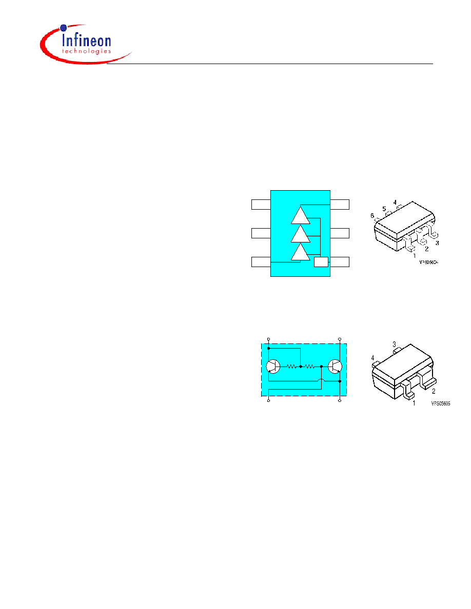
2. Description of BGA430 and BGB540
The BGA430 is a three-stage, 50 ohm, internally
matched, unconditionally stable MMIC fabricated
in Infineon's well-proven, consistent and cost-
effective 25 GHz transition frequency (f
T
) B6HF
bipolar process. The BGA430 only requires
three external elements input / output DC
blocking capacitors, and a single decoupling
capacitor on the power supply pin. Depending
on the particular LNB performance
requirements, the BGA430 may be used as a
stand-alone I.F. amplifier block, or together with
the BGB540.
The BGB540 is an unmatched, active-biased RF
transistor produced in the 45 GHz f
T
B6Hfe
bipolar process. B6Hfe, derived from B6HF, is a
more advanced process with higher achievable
gains and lower noise figures. BGB540 uses an
internal current mirror for DC biasing. This
approach achieves some reduction in external
component count due to elimination of a number
of external DC bias circuit elements, while still
preserving the flexibility inherent in a fully
discrete transistor. The device bias current may
be adjusted via a single external resistor.
Furthermore, the internal current-mirror, being
located on the same chip as the RF transistor
cell, has excellent "thermal tracking" of the RF
transistor cell, providing for a more stable DC
operating point over temperature. The BGB540
preserves the cost-advantages of the simple 4-
pin industry-standard SOT343 package.
A block diagram and package drawing for the
BGA430 and BGB540 are given in Figures 1 &
2, respectively. Note that for the BGB540, the
emitter areas of the current-mirror transistor cell
and the RF transistor cell are in the ratio of 1:10.
To set DC bias current for the BGB540, one
injects a current into pin 4, and the current
drawn by the RF transistor cell is 10 times the
current injected into pin 4, by virtue of the
current-mirror principle. The simplest DC bias
configuration for BGB540 involves using just a
single resistor between the power supply and
pin 4 no RF choke or decoupling capacitor is
required on pin 4. The value of this bias resistor
referred to as " R
BIAS
" required for a given
device current can be determined from curves
given in the BGB540 datasheet. For lower
operating currents, the value of R
BIAS
becomes
large, and therefore R
BIAS
in series with the
power supply voltage behaves as a near-ideal
constant-current source. Otherwise, the
BGB540 is treated like a standard RF transistor,
with the normal procedures for impedance
matching, stability analysis, etc. being used.
Figure 1. BGA430 Block Diagram and
Package (SOT363).
Figure 2. BGB540 Block Diagram and
Package (SOT343).
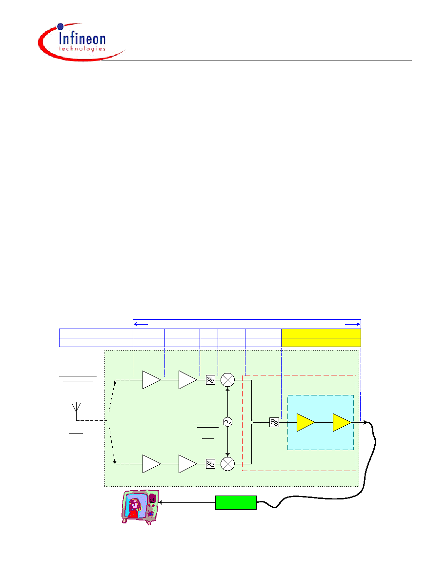
3. General DBS System Information
A generic block diagram of a Direct Broadcast
Satellite Low Noise Block Amplifier /
Downconverter (LNB) is given in Figure 3 on
page 3. LNBs produced for the Direct Broadcast
Satellite consumer electronics market are
extraordinarily cost-sensitive, and cost issues
are usually the primary consideration in the LNB
design process.
A broadcast signal in the 12 GHz range is
transmitted from an orbiting satellite towards the
Earth's surface. There are two orthogonal parts
Base
Pin 1
1/10 BFP540
BFP540
Bias
Pin 4
C
Pin 3
Emitter
Pin 2
BGB 540 B6HFe
V
CE
MAX
= 4.5 V
I
C MAX
= 80 mA
5
GND1
4
GND2
6
RFin
2
GND1
3
RFout
1
Vcc
Bias
BGA430 (B6HF) V
MAX
= 6.5 V, I
MAX
= 35 mA
AN 074 Rev E 3 / 24 19-November-2002
Applications Note No. 074
Silicon Discretes
of the composite signal a vertically polarized
component, and a horizontally polarized
component. The two polarizations enable more
efficient use of the available bandwidth and
power. (The isolation between "vertical" and
"horizontal" radio signals permits a greater
number of channels to be simultaneously
broadcast within the available bandwidth than
would otherwise be expected.) The satellite's
transmitted signal is received by an earth-based
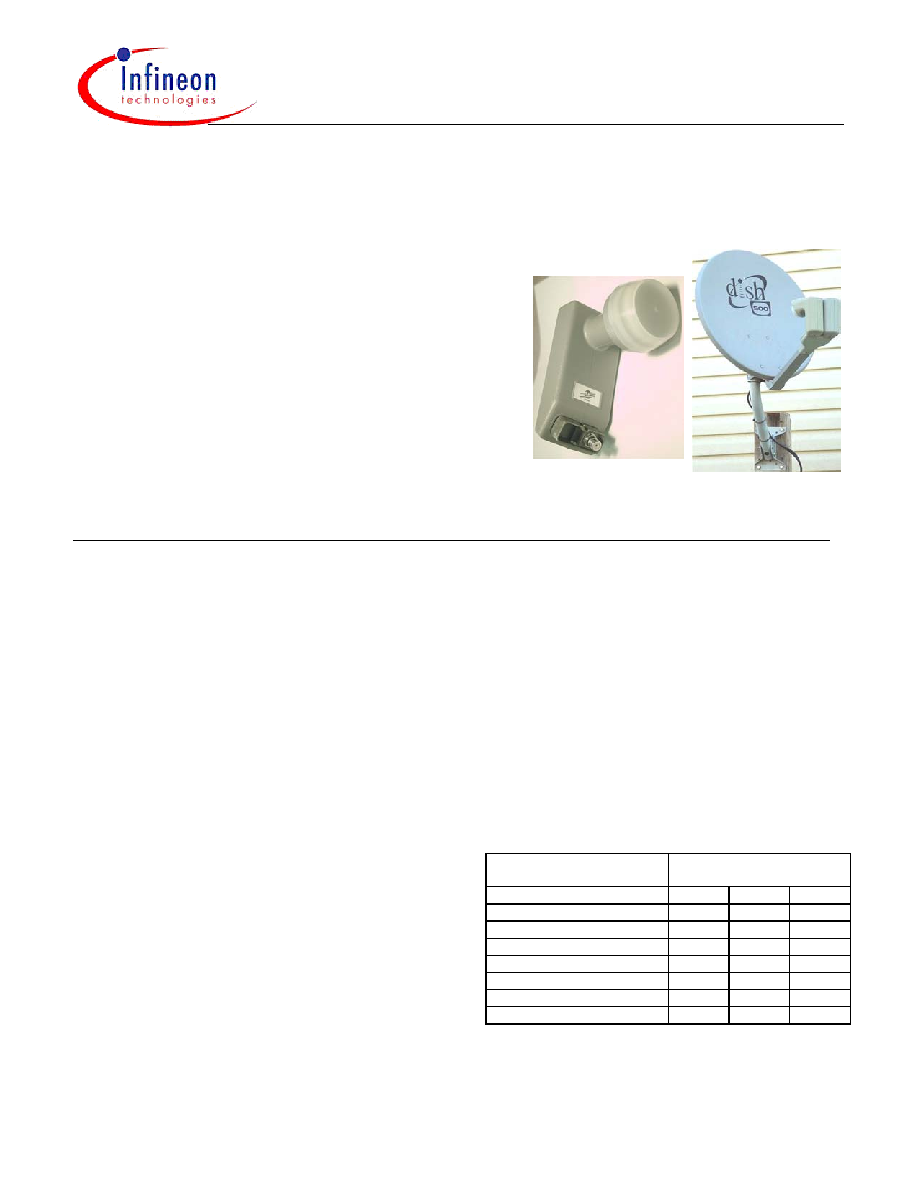
antenna like that shown in the photo on page 1.
The signal is focused by the parabolic "dish"
antenna onto a waveguide integrated into the
LNB. The received signal travels a short
distance down the waveguide until reaching a
waveguide-to-microstripline transition that
carries the signal onto the LNB circuit board
assembly.
The LNB must be able to receive channels on
both the vertically and horizontally polarized
signals and one way to do this is to have
essentially two different receiver front-ends as
shown in Figure 3 below.
Various approaches and switching schemes are
employed in different LNB designs to enable the
end user(s) to select between channels riding on
either the horizontally or vertically polarized
signals. Each approach has its own unique cost
and performance trade-offs. Optimizing LNB
architectures to achieve performance
requirements while continuously reducing cost
as new, higher-performance and lower cost
semiconductor devices become available is a
challenging task.
A further complication to the switching
requirements is added if one wishes to have a
"dual output LNB" e.g. an LNB that can drive
two different set-top boxes and television sets
simultaneously, allowing each TV to display a
different channel. ("Quad output" LNBs are also
available). One possible switching scheme for a
"single output LNB" is shown in Figure 3. Note
that the vertical / horizontal switching is done at
the I.F. Amplifier block. The BGA430 and
BGB540 are shown in the shaded I.F. Amplifier
section.
Figure 3. Generic Block Diagram, "Single Output" Direct
Broadcast Satellite Television Block Downconverter (DBS LNB)
LNA
LNA
LNA
LNA
Horizontal
Polarization
Vertical
Polarization
BPF
BPF
(V
ert
.
/
H
o
r.
)
Switch
BPF
Mixer
(Passive or Active)
Intermediate Frequency ("I.F.")
950 - 1450 MHz (North America)
950 - 2150 MHz (Europe, Asia)
IF Amp
IF Amp
75 ohm Coaxial Cable
To Set-Top Box
(75 ohm system)
RG-6, RG-6/U
BGA430 + BGB540
I.F. Amplifier
"Set Top Box"
(Channel Selector,
Demodulator, etc.)
Audio + Video
to TV set
LNB
(Components in Shaded Area)
Mixer
(Passive or Active)
4
Approximate Gain, dB =>
Approximate Noise Figure, dB =>
10
0.5
12
0.7
-1.5
1.5
-10 to +8
7 to 12
- 4
30 to 45
3 to 7
U.S., Japan, Korea,
Latin America
11.45 - 12.75 GHz
(depending on region)
Europe
10.7 - 12.75 GHz
(Two L.O.'s required for
full coverage)
U.S., Japan, Korea,
Latin America:
in 10.5 - 11.25 GHz range
Europe:
10.6 GHz or
9.75 + 10.6 GHz
(dual DRO)
Local Oscillator
(DRO)
Cascaded Gain: approximately 55 - 60 dB; Cascaded Noise Figure: approximately 1 dB

AN 074 Rev E 4 / 24 19-November-2002
Applications Note No. 074
Silicon Discretes
After the waveguide to microstrip transition, the
signals enter a PC Board assembly. The signal
is amplified in two or more low noise amplifier
(LNA) stages and then hits a band pass filter.
The LNAs provide enough gain to boost the
level of the received signal such that the overall
receiver noise figure is dominated by the LNA
block itself. The LNA stages must have enough
gain and a sufficiently low noise figure to
minimize the noise floor for the entire receive
chain. Achieving enough gain and a low enough
noise figure at 12 GHz is costly, and anything
that can reasonably be done to relax the
requirements on the LNA section will reduce
cost.
The LNA is then followed by a band pass filter
(BPF) which provides for some rejection of out
of-band signals and noise, as well as image
rejection. The amplified and filtered signal then
enters the mixer stage.
The types of simple, inexpensive mixers likely to
be used in an LNB will usually convert both the
desired input signal (12 GHz in this case) and an
undesired "image" frequency (10 GHz) to the
intermediate frequency (1 GHz for this example).
The band pass filter in front of the mixer stage
can attenuate any undesired signals or noise
present at the 10 GHz image frequency before it
hits the mixer stage, preventing the undesired
image from being down-converted on top of the
desired, down-converted 12 GHz input signal.
At present, most LNB manufacturers use one of
three main types of mixers:
1. GaAs FET used as a simple active mixer
2. GaAs FET with no DC bias applied ( "FET
resistive mixer")
3. Schottky Diode based mixer
Some references for mixers are given in [1] and
[2] at the end of this applications note.
The FET active mixer will usually have
"conversion gain" while the FET resistive mixer
or Schottky diode mixers have "conversion loss".
Conversion gain or loss is simply the ratio of the
amplitudes of the down-converted output I.F.
signal to the RF input signal. A poor noise figure
in the mixer stage, as well as high conversion
loss, places additional demands (and cost) on
both the LNA block up front, as well as the I.F.
amplifier which follows.
The down-converted I.F. signal undergoes
further band pass filtering and then is amplified
in the I.F. amplifier block. The I.F. amplifier is
the focus of this applications note, and is the
primary point of discussion regarding the
BGA430 and BGB540 Silicon MMICs. The I.F.
amplifier boosts the signal up to a reasonable
input level for the set top box. It is worth noting
that the system impedance in this area is 75
ohms, not 50 ohms, and that the coaxial cable
typically used (RG-6, RG-6/U or sometimes RG-
59) is very low cost, and has a relatively high
attenuation per unit length a the intermediate
frequency. Furthermore, the attenuation of the
cable increases with increasing frequency
coaxial cable loss at 2150 MHz is higher than
cable loss at 950 MHz. Herein lies the reason
for designing an I.F. amplifier with a gain
slope that increases with increasing
frequency this positive gain slope in the
I.F. amp will help to compensate out the
negative gain slope of the coaxial cable and
other RF front-end blocks.
4. Information on Printed Circuit Board
The PC board used in this applications note was
simulated within and generated from the
Eagleware GENESYS
®
[3] software package.
After simulations, CAD files required for PCB
fabrication, including Gerber 274X and Drill files,
were created within and output from GENESYS.
Photos of the PC board are provided in Figures
4, 5 and 6. A cross-sectional diagram is given
in Figure 7. A schematic diagram and a Bill Of
Material (BOM) for the complete BGA430 +
BGB540 I.F. Amplifier are given in Figures 8
and 9, respectively. The PC Board material
used is standard FR4. Note that each MMIC
may be tested individually; capacitor C3 (see
schematic) may be positioned to "steer" the RF
from the BGA430 output to the SMA connector
on the bottom of the PCB, or, C3 may be used
to link the track from this same RF connector to
the input of the BGB540. When testing the
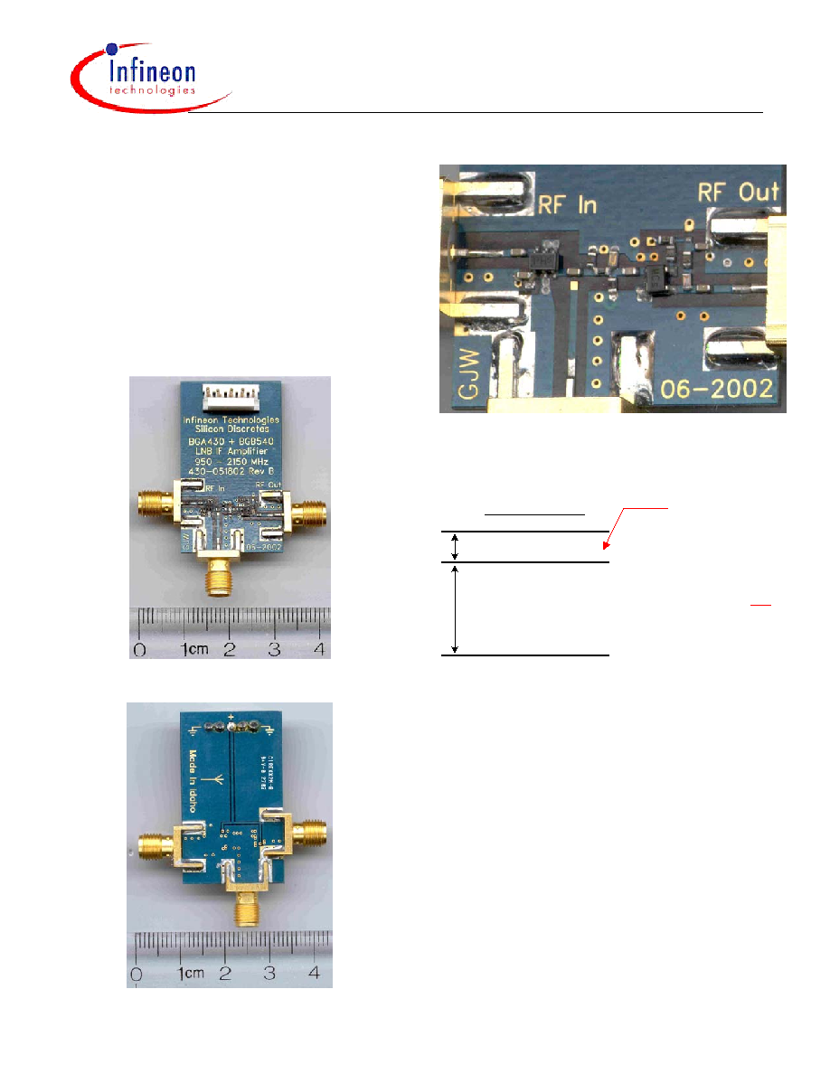
AN 074 Rev E 5 / 24 19-November-2002
Applications Note No. 074
Silicon Discretes
BGB540 stage alone, a zero-ohm "jumper"
needs to be used in place of R2. The total PCB
area consumed for the entire BGA430 +
BGB540 I.F. Amplifier is approximately 0.585 x
0.180 inch / 14.9 x 4.6 mm, or approximately 70
mm
2
. The total component count, including
both Silicon MMICs, is 16. Note that PCB area
and component count may be reduced markedly
if the end user is able to satisfy his or her I.F.
amplifier requirements by using the BGA430 as
a stand-alone part. The next section describes
the BGA430 as a stand-alone I.F. amplifier.
Figure 4. Top View of I.F. Amp PC Board.
Figure 5. Bottom View of I.F. Amp PC Board
Figure 6. Close-In Shot of PCB. BGA430 on
left, BGB540 on Right.
Figure 7. Cross-Section Diagram of I.F.
Amplifier Printed Circuit Board.
BOTTOM LAYER
0.010 inch / 0.254 mm
0.031 inch / 0.787 mm ?
PCB CROSS SECTION
TOP LAYER
INTERNAL GROUND PLANE
LAYER FOR MECHANICAL RIGIDITY OF PCB,
THICKNESS HERE NOT
CRITICAL AS LONG AS TOTAL PCB THICKNESS DOES NOT EXCEED
0.045 INCH / 1.14 mm (SPECIFICATION FOR TOTAL PCB THICKNESS:
0.040 + 0.005 / - 0.005 INCH; 1.016 + 0.127 mm / - 0.127 mm )
THIS SPACING CRITICAL !
5. Using the BGA430 as a Stand-Alone I.F.
Amplifier Block
Provided that BGA430 gain magnitude, gain
curve and output power are adequate for the
user's LNB system requirements, BGA430 may
be used as a very low-parts-count, low-cost
stand-alone LNB I.F. amplifier over the 950
2150 MHz range. Note that only 3 external
elements are typically required with BGA430:
1) an input DC blocking capacitor 2) an output
DC blocking capacitor 3) an RF bypass / RF
decoupling capacitor on the V
CC
pin (Pin 1).
Table 2 on page 8 summarizes the BGA430's
typical performance and Figures 11 15 give
network analyzer screen shots of input / output
match, gain, and (continued on page 7)