Application Note
1
V3.0, 2001-10
The BGA622 Silicon-Germanium
Universal Low Noise Amplifier MMIC
in 1800 - 2500 MHz Receiver Applications
1
2
4
3
SOT-343
Silicon Discretes
Application Note No. 069
Features
· Versatile, easy-to-use LNA MMIC
in 70 GHz
f
t
SiGe technology
· 50
matched output, pre-matched input
· Integrated output DC blocking capacitor,
integrated RF choke on internal bias network
· Low current consumption of 6 mA
· "Shutdown" or "Sleep" mode
· Unconditionally stable
· Low external component count
· Exceptional noise figure: 1.1 dB in a PC board at 2 GHz
Applications
· Low Noise Amplifier for 800/900 MHz, GSM900, 900 MHz ISM, DCS1800, GPS,
1900 MHz PCS, 2.1 GHz UMTS and 2.4 GHz Wireless LAN
· Long-Range Bluetooth applications requiring improved system sensitivity via use of
an external LNA
Introduction
The BGA622 is an easy-to-use, versatile and flexible low-cost Low Noise Amplifier
(LNA) MMIC designed for the high linearity and sensitivity requirements of existing and
next - generation wireless applications including GSM, 900 MHz ISM, GPS, UMTS and
Wireless LANs. Based on Infineon's cost-effective 70 GHz
f
T
Silicon-Germanium (SiGe)
B7HF bipolar process technology, the BGA622 offers a 1.1 dB noise figure and 15 dB of
gain at 2.1 GHz for high performance, cost-effective mobile communications
applications. BGA622 offers impressive noise figure performance, particularly for a low-
cost, integrated MMIC. In the past, in-circuit noise figures approaching 1.0 dB at 2 GHz
were possible only for more expensive GaAs-based, fully discrete solutions utilizing
narrowband impedance matching and higher external parts count. The BGA622
combines the excellent noise figure advantages of a high-performance discrete solution
with the ease-of-use, low parts count, and diminished risk and reduced system
development time made possible by a MMIC approach.
Application Note
2
V3.0, 2001-10
The BGA622 Silicon-Germanium Universal Low Noise
Amplifier MMIC in 1800 - 2500 MHz Receiver Applications
Introduction
The new LNA incorporates a 50
matched output with an integrated output DC blocking
capacitor. The broadband output match simplifies integration issues with external image-
stripping filters. The input is pre-matched, requiring an external DC blocking capacitor.
An integrated, on-chip inductor eliminates the need for an external RF choke on the
voltage supply pin. The noise figure of BGA622 is relatively insensitive to the input
impedance matching approach taken by the end user, reducing development time and
risk. A low supply current of 6 mA at 2.75 V and an integrated on/off feature provides for
low power consumption and increased stand by time for 3G cellular handsets or other
portable, battery-operated wireless applications.
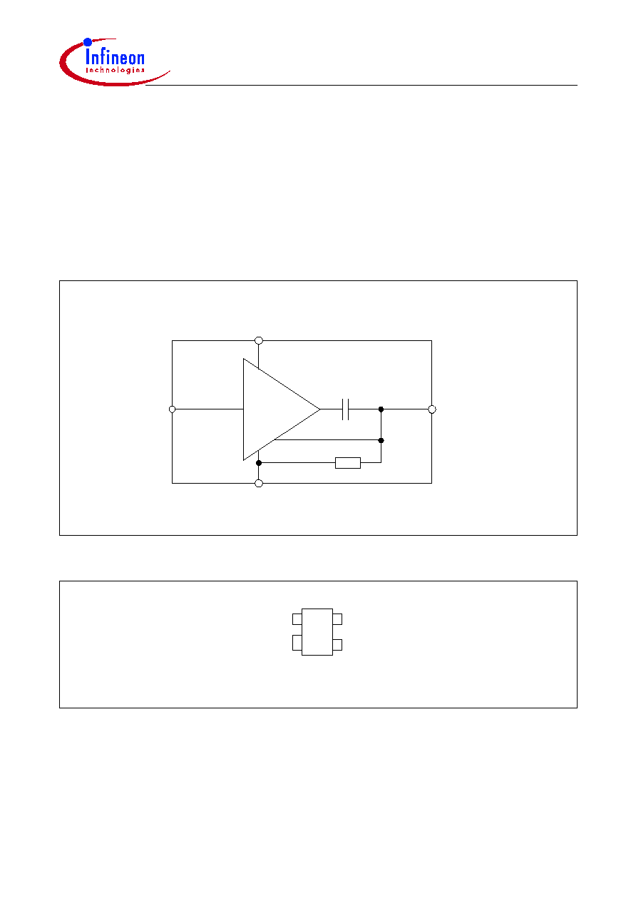
Figure 1
BGA622's Equivalent Circuit
Figure 2
Pin Connections
Vcc,4
Out,3
GND,2
In,1
On/Off
10k
In, 1
4, Vcc
Top View
GND, 2
3, Out
Application Note
3
V3.0, 2001-10
The BGA622 Silicon-Germanium Universal Low Noise
Amplifier MMIC in 1800 - 2500 MHz Receiver Applications
Overview
Overview
The BGA622 is shown in three different configurations for the frequency band between
1700 MHz and 2500 MHz which covers the PCN/PCS, UMTS and BlueTooth
frequencies at 1800 / 1900 MHz, 2.14 GHz and 2.4 GHz:
· Configuration A: minimum parts count, power down option is not used
· Configuration B: BGA622 with power down option
· Configuration C: BGA622 with power down option and increased IIP
3
The following table shows the measured performance of these three circuits. All
measurement values presented in this application note include losses of both PCB and
connectors - in other words, the reference planes used for measurements are the PCB's
RF SMA connectors. Noise figure and gain results shown do not have any PCB loss
extracted from them.
Performance Overview
Parameter
Configuration A
Configuration B
Configuration C
Supply voltage
2.75 V
2.75 V
2.75 V
Supply current
5.5 mA
5.4 mA
5.4 mA
Gain
14.8 dB @ 1.85 GHz
13.8 dB @ 2.14 GHz
12.6 dB @ 2.4 GHz
14.5 dB @ 1.85 GHz
13.5 dB @ 2.14 GHz
12.5 dB @ 2.4 GHz
14.6 dB @ 1.85 GHz
13.5 dB @ 2.14 GHz
12.5 dB @ 2.4 GHz
Noise Figure
1.2 dB @ 1.85 GHz
1.25 dB @ 2.14 GHz
1.3 dB @ 2.4 GHz
1.2 dB @ 1.85 GHz
1.2 dB @ 2.14 GHz
1.35 dB @ 2.4 GHz
1.2 dB @ 1.85 GHz
1.25 dB @ 2.14 GHz
1.3 dB @ 2.4 GHz
Input return loss
11.1 dB @ 1.85 GHz
12.5 dB @ 2.14 GHz
11.6 dB @ 2.4 GHz
11.9 dB @ 1.85 GHz
12.3 dB @ 2.14 GHz
11.2 dB @ 2.4 GHz
14.1 dB @ 1.85 GHz
13.1 dB @ 2.14 GHz
11.1 dB @ 2.4 GHz
Output return loss 12.4 dB @ 1.85 GHz
12.5 dB @ 2.14 GHz
12.8 dB @ 2.4 GHz
12.2 dB @ 1.85 GHz
11.4 dB @ 2.14 GHz
11.0 dB @ 2.4 GHz
11.7 dB @ 1.85 GHz
11.3 dB @ 2.14 GHz
11.0 dB @ 2.4 GHz
Reverse Isolation
26.1 dB @ 1.85 GHz
24.8 dB @ 2.14 GHz
23.8 dB @ 2.4 GHz
26.3 dB @ 1.85 GHz
25.0 dB @ 2.14 GHz
24.0 dB @ 2.4 GHz
26.2 dB @ 1.85 GHz
25.0 dB @ 2.14 GHz
24.1 dB @ 2.4 GHz
Input compression
point
1)
1)
Measured at 2.14 GHz
-15 dBm
-16 dBm
-15 dBm
Input 3
rd
order
intercept point
2)
2)
-30 dBm per tone,
f
= 1 MHz
-7.1 dBm @ 1.8 GHz
-5.5 dBm @ 2.14 GHz
-3.9 dBm @ 2.4 GHz
-6.6 dBm @ 1.8 GHz
-4.0 dBm @ 2.14 GHz
-3.9 dBm @ 2.4 GHz
4.7 dBm @ 1.8 GHz
4.4 dBm @ 2.14 GHz
4.3 dBm @ 2.4 GHz
Application Note
4
V3.0, 2001-10
The BGA622 Silicon-Germanium Universal Low Noise
Amplifier MMIC in 1800 - 2500 MHz Receiver Applications
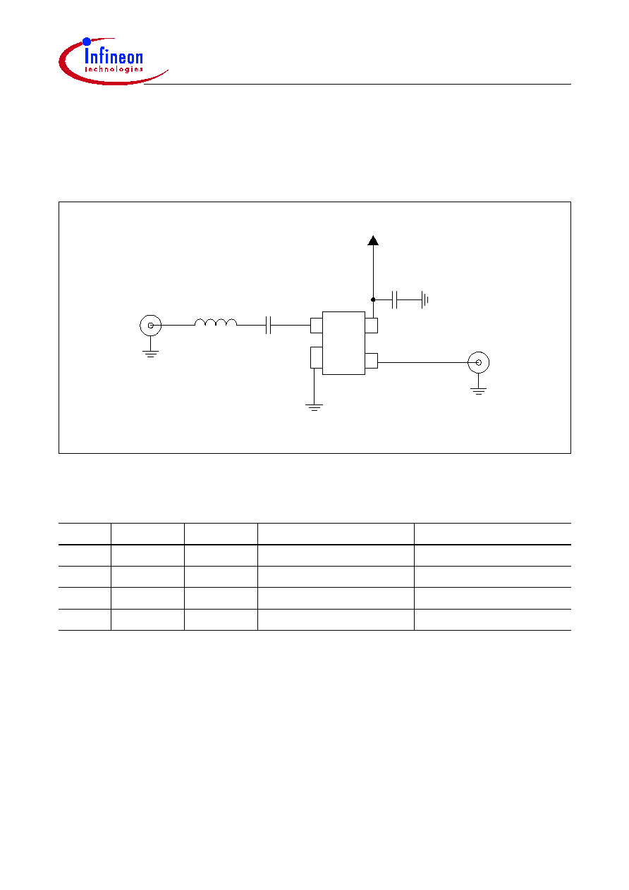
Configuration A
Configuration A
The circuit in
Figure 3
shows the minimum parts count version of a BGA622 LNA. There
are only three external elements necessary. A DC blocking capacitor at the output and
a coil at the power supply are already integrated on chip
Figure 3
Circuit Diagram of Configuration A
For measurement graphs of configuration A please refer to the next pages.
Bill of Materials of Configuration A
Name
Value
Package
Manufacturer
Function
C
1
47 pF
0402
various
DC block
C
3
47 pF
0402
various
RF bypass
L
1
2.2 nH
0402
Toko LL1005-FH
Input matching
Q1
BGA622
SOT-343
Infineon Technologies
SiGe MMIC
C1
47pF
1
2
3
4
Q1
BGA622
Out
C3
47pF
Vcc
In
L1
2.2nH

Application Note
5
V3.0, 2001-10
The BGA622 Silicon-Germanium Universal Low Noise
Amplifier MMIC in 1800 - 2500 MHz Receiver Applications
Configuration A
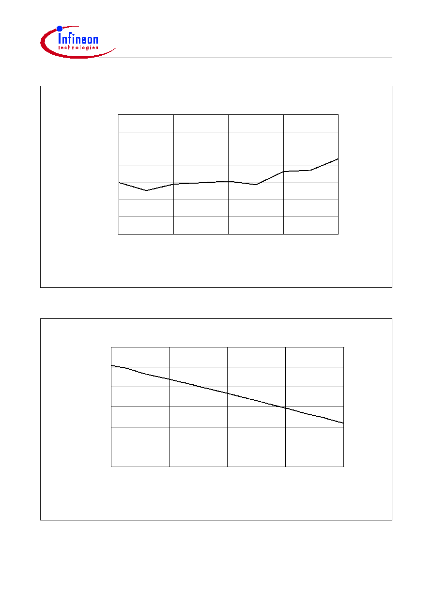
Figure 4
Noise Figure Configuration A
Figure 5
Gain Configuration A
0,6
0,8
1
1,2
1,4
1,6
1,8
2
1,7
1,9
2,1
2,3
2,5
Frequency [GHz]
Noise Figure [dB]
10
11
12
13
14
15
16
1,7
1,9
2,1
2,3
2,5
Frequency [GHz]
Gain [dB]

Application Note
6
V3.0, 2001-10
The BGA622 Silicon-Germanium Universal Low Noise
Amplifier MMIC in 1800 - 2500 MHz Receiver Applications
Configuration A
Figure 6
Return Loss Configuration A
Figure 7
Reverse Isolation Configuration A
6
8
10
12
14
16
1,7
1,9
2,1
2,3
2,5
Frequency [GHz]
Return Loss [dB]
s11
s22
20
22
24
26
28
1,7
1,9
2,1
2,3
2,5
Frequeny [GHz]
Reverse Isolation [dB]

Application Note
7
V3.0, 2001-10
The BGA622 Silicon-Germanium Universal Low Noise
Amplifier MMIC in 1800 - 2500 MHz Receiver Applications
Configuration A
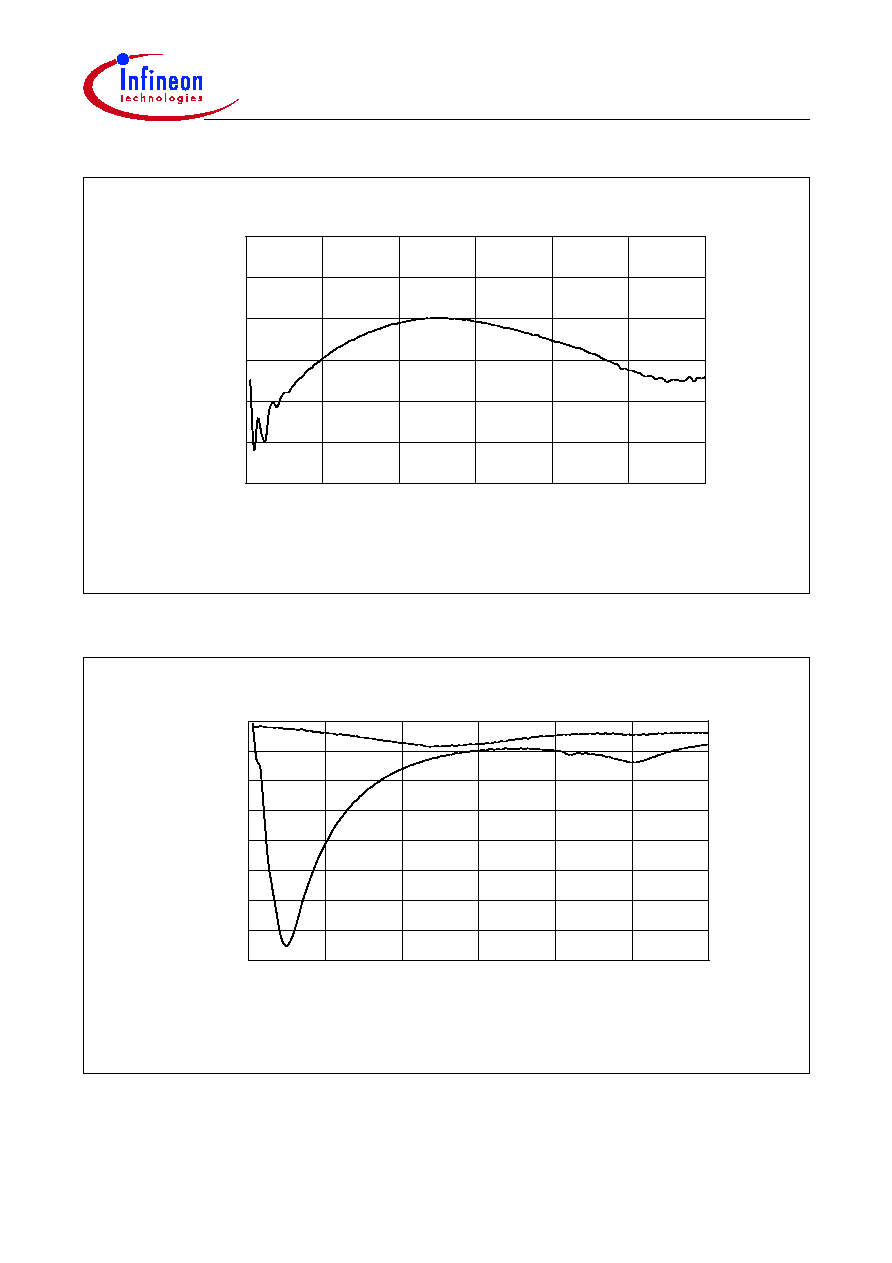
Figure 8
Stability Factor K and Stability Measure B1 of Configuration A
Figure 9
Wide Span Gain Configuration A
0
1
2
3
4
5
0
1
2
3
4
5
6
Frequency [GHz]
K, B1
K
B1
0
2
4
6
8
10
12
14
16
18
20
0
1
2
3
4
5
6
Frequency [GHz]
Gain [dB]

Application Note
8
V3.0, 2001-10
The BGA622 Silicon-Germanium Universal Low Noise
Amplifier MMIC in 1800 - 2500 MHz Receiver Applications
Configuration A
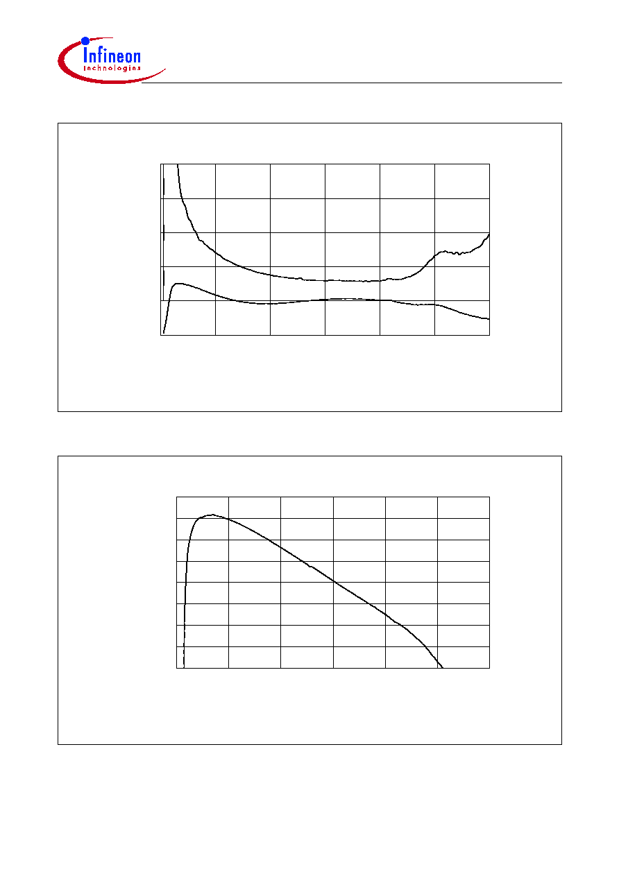
Figure 10
Wide Span Return Loss Configuration A
Figure 11
Gain Compression @ 2.14 GHz Configuration A
0
2
4
6
8
10
12
14
16
18
20
0
1
2
3
4
5
6
Frequency [GHz]
Return Loss [dB]
s11
s22
-25
-20
-15
-10
-5
0
-35
-30
-25
-20
-15
-10
P
in
[dBm]
P
out
[dBm]
10
11
12
13
14
15
Gain [dB]
Gain
P
out

Application Note
9
V3.0, 2001-10
The BGA622 Silicon-Germanium Universal Low Noise
Amplifier MMIC in 1800 - 2500 MHz Receiver Applications
Configuration B
Configuration B
Figure 12
shows a BGA622 LNA with available power down mode. In the BGA622, an
internal high-impedance path exists around the device's internal output DC blocking
capacitor, between the output pin and the device's internal shutdown circuitry. Applying
V
cc
at the Output pin (pin 3) will switch off the BGA622 and only a small supply current
of about 0.26 mA flows into the device in shutdown mode. The schematic shows the
"PD" (Power Down) connection where the shutdown signal may be applied. Ground or
an open circuit at the PD pin will turn on the device. Note that if the Power Down feature
is employed, the internal DC blocking capacitor of the BGA622 is bypassed by external
circuitry, and therefore some sort of external DC blocking at the output must be
employed. This can be either an external output DC blocking capacitor, or the usual
image-stripping filter, provided the input of the filter presents a DC open circuit.
Figure 12
Circuit Diagram Configuration B
Bill of Materials of Configuration B
Name
Value
Package
Manufacturer
Function
C
1
47 pF
0402
various
DC block
C
3
47 pF
0402
various
RF bypass
C
4
47 pF
0402
various
DC block
C
5
47 pF
0402
various
RF bypass
L
1
2.2 nH
0402
Toko LL 1005-FH
Input matching
L
3
47 nH
0402
Toko LL 1005-FH
RF block
Q1
BGA622
SOT-343
Infineon Technologies
SiGe MMIC
C1
47pF
C4
47pF
C5
47pF
L3
47nH
1
2
3
4
Q1
BGA622
Out
C3
47pF
Vcc
In
L1
2.2nH
PD
Application Note
10
V3.0, 2001-10
The BGA622 Silicon-Germanium Universal Low Noise
Amplifier MMIC in 1800 - 2500 MHz Receiver Applications
Configuration B
Figure 13
Noise Figure Configuration B
Figure 14
Gain Configuration B
0,6
0,8
1
1,2
1,4
1,6
1,8
2
1,7
1,9
2,1
2,3
2,5
Frequency [GHz]
Noise Figure [dB]
10
11
12
13
14
15
16
1,7
1,9
2,1
2,3
2,5
Frequency [GHz]
Gain [dB]

Application Note
11
V3.0, 2001-10
The BGA622 Silicon-Germanium Universal Low Noise
Amplifier MMIC in 1800 - 2500 MHz Receiver Applications
Configuration B
Figure 15
Return Loss Configuration B
Figure 16
Reverse Isolation Configuration B
6
8
10
12
14
16
1,7
1,9
2,1
2,3
2,5
Frequency [GHz]
Return Loss [dB]
s11
s22
20
22
24
26
28
1,7
1,9
2,1
2,3
2,5
Frequeny [GHz]
Reverse Isolation [dB]
Application Note
12
V3.0, 2001-10
The BGA622 Silicon-Germanium Universal Low Noise
Amplifier MMIC in 1800 - 2500 MHz Receiver Applications
Configuration B
Figure 17
Stability Factor K and Stability Measure B1 of Configuration B
Figure 18
Wide Span Gain Configuration B
0
1
2
3
4
5
0
1
2
3
4
5
6
Frequency [GHz]
K, B1
K
B1
0
2
4
6
8
10
12
14
16
18
20
0
1
2
3
4
5
6
Frequency [GHz]
Gain [dB]

Application Note
13
V3.0, 2001-10
The BGA622 Silicon-Germanium Universal Low Noise
Amplifier MMIC in 1800 - 2500 MHz Receiver Applications
Configuration B
Figure 19
Wide Span Return Loss Configuration B
Figure 20
Gain Compression @ 2.14 GHz Configuration B
0
2
4
6
8
10
12
14
16
18
20
0
1
2
3
4
5
6
Frequency [GHz]
Return Loss [dB]
s11
s22
-25
-20
-15
-10
-5
0
-35
-30
-25
-20
-15
-10
P
in
[dBm]
P
out
[dBm]
10
11
12
13
14
15
Gain [dB]
Gain
P
out
Application Note
14
V3.0, 2001-10
The BGA622 Silicon-Germanium Universal Low Noise
Amplifier MMIC in 1800 - 2500 MHz Receiver Applications
Configuration B
Figure 21
Forward Transmission in Power Down Mode
Figure 22
Input and Output Return Loss in Power Down Mode
-60
-50
-40
-30
-20
-10
0
0
1
2
3
4
5
6
Frequency [GHz]
Forward Transmission [dB]
0
2,5
5
7,5
10
12,5
15
17,5
20
0
1
2
3
4
5
6
Frequency [GHz]
Return Loss [dB]
s11
s22

Application Note
15
V3.0, 2001-10
The BGA622 Silicon-Germanium Universal Low Noise
Amplifier MMIC in 1800 - 2500 MHz Receiver Applications
Configuration C
Configuration C
The circuit in
Figure 23
shows a way to increase the input 3
rd
order intercept point of
BGA622.
L
2
and
C
2
offer low-frequency intermodulation products a low impedance path
to ground. This prevents them from modulating the base voltage of the BGA622's
internal RF transistor and thus linearity is improved. Typically the input 3
rd
-order intercept
point of BGA622 can be improved by 6 to 10 dB in this manner.
Figure 23
Circuit Diagram Configuration C
Bill of Materials of Configuration C
Name
Value
Package
Manufacturer
Function
C
1
47 pF
0402
various
DC block
C
2
100 nF
0603
various
IIP
3
improvement
C
3
47 pF
0402
various
RF bypass
C
4
47 pF
0402
various
DC block
C
5
47 pF
0402
various
RF bypass
L
1
2.2 nH
0402
Toko LL 1005-FH
Input matching
L
2
22 nH
0402
Toko LL 1005-FH
RF block
L
3
47 nH
0402
Toko LL 1005-FH
RF block
Q1
BGA622
SOT-343
Infineon Technologies
SiGe MMIC
C1
47pF
C4
47pF
C5
47pF
L3
47nH
1
2
3
4
Q1
BGA622
Out
C2
100nF
L2
22nH
C3
47pF
Vcc
In
L1
2.2nH
PD

Application Note
16
V3.0, 2001-10
The BGA622 Silicon-Germanium Universal Low Noise
Amplifier MMIC in 1800 - 2500 MHz Receiver Applications
Configuration C
Figure 24
Noise Figure Configuration C
Figure 25
Gain Configuration C
0,6
0,8
1
1,2
1,4
1,6
1,8
2
1,7
1,9
2,1
2,3
2,5
Frequency [GHz]
Noise Figure [dB]
10
11
12
13
14
15
16
1,7
1,9
2,1
2,3
2,5
Frequency [GHz]
Gain [dB]

Application Note
17
V3.0, 2001-10
The BGA622 Silicon-Germanium Universal Low Noise
Amplifier MMIC in 1800 - 2500 MHz Receiver Applications
Configuration C
Figure 26
Return Loss Configuration C
Figure 27
Reverse Isolation Configuration C
6
8
10
12
14
16
1,7
1,9
2,1
2,3
2,5
Frequency [GHz]
Return Loss [dB]
s11
s22
20
22
24
26
28
1,7
1,9
2,1
2,3
2,5
Frequeny [GHz]
Reverse Isolation [dB]
Application Note
18
V3.0, 2001-10
The BGA622 Silicon-Germanium Universal Low Noise
Amplifier MMIC in 1800 - 2500 MHz Receiver Applications
Configuration C
Figure 28
Stability Factor K and Stability Measure B1 of Configuration C
Figure 29
Wide Span Gain Configuration C
0
1
2
3
4
5
0
1
2
3
4
5
6
Frequency [GHz]
K, B1
K
B1
0
2,5
5
7,5
10
12,5
15
17,5
20
0
1
2
3
4
5
6
Frequency [GHz]
Gain [dB]
Application Note
19
V3.0, 2001-10
The BGA622 Silicon-Germanium Universal Low Noise
Amplifier MMIC in 1800 - 2500 MHz Receiver Applications
Configuration C
Figure 30
Wide Span Return Loss Configuration C
Figure 31
Gain Compression @ 2.14 GHz Configuration C
0
2
4
6
8
10
12
14
16
18
0
1
2
3
4
5
6
Frequency [GHz]
Return Loss [dB]
s11
s22
-25
-20
-15
-10
-5
0
-35
-30
-25
-20
-15
-10
P
in
[dBm]
P
out
[dBm]
10
11
12
13
14
15
Gain [dB]
Gain
P
out
Application Note
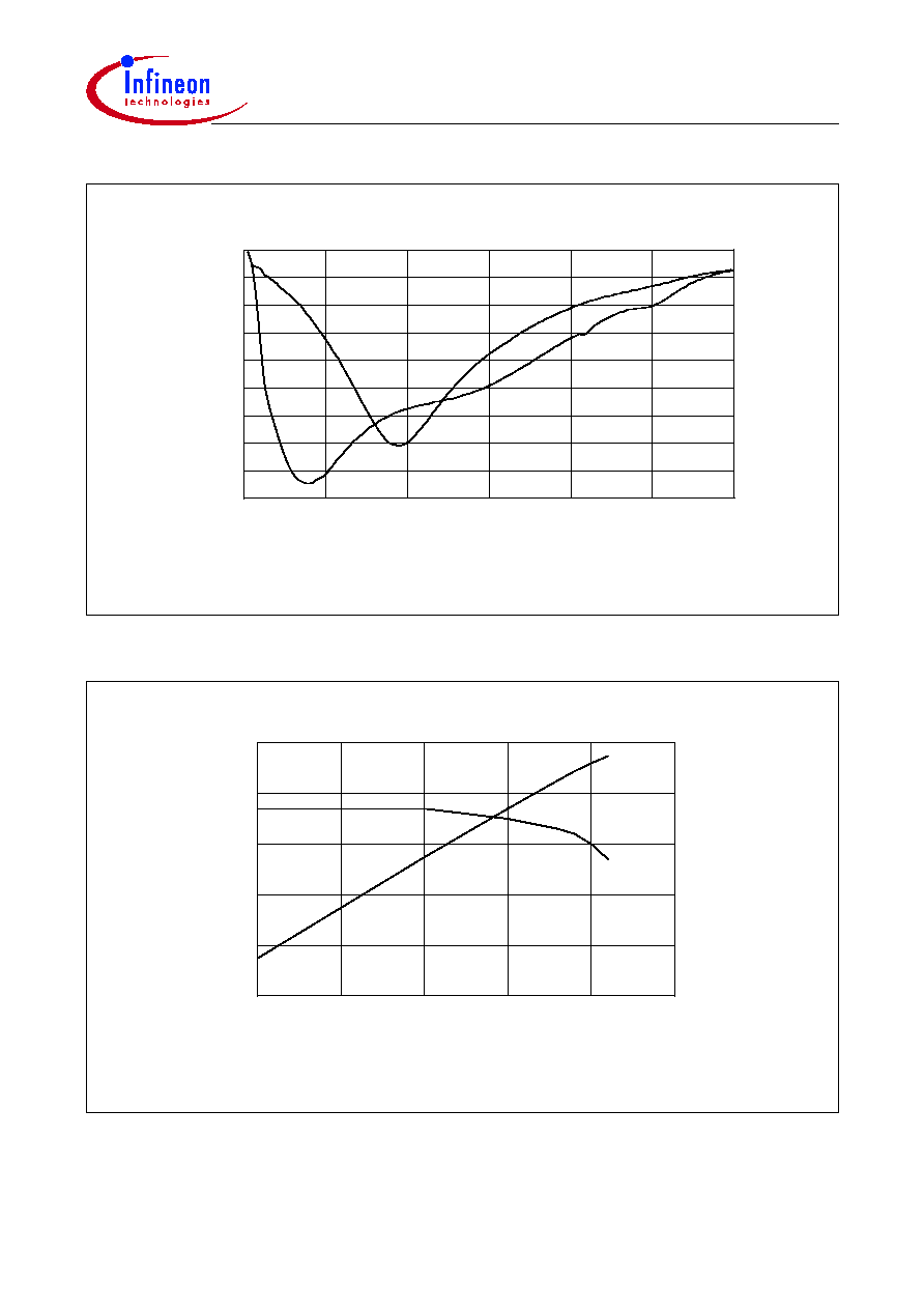
20
V3.0, 2001-10
The BGA622 Silicon-Germanium Universal Low Noise
Amplifier MMIC in 1800 - 2500 MHz Receiver Applications
Application PCB
Application PCB
Figure 32
shows the placement of the specific components on the PCB. To place
L
1
on
the board the input 50
transmission line has to have a gap cut in it to allow for the
insertion of
L
1
. For this purpose a relief is provided in the solder mask to ease the
soldering of the component.
Figure 32
Component Placement on Application PCB
Figure 33
PCB Cross Section
Evaluation boards for the LNA applications described in this application note are
available from Infineon Technologies.
C1
Q1
1
2
3
4
C2
C3
C4
C5
L1
L3
8 mm
9.
5 mm
L2
NA
NA
NA
In
Out
PD
Vcc
0.8 mm FR4
0.2 mm FR4
35 µm Cu
35 µm Cu
35 µm Cu
for mechanical
rigidity of PCB

Edition 2001-10
Published by Infineon Technologies AG,
St.-Martin-Strasse 53,
81669 München, Germany
©
Infineon Technologies AG 2002.
All Rights Reserved.
Attention please!
The information herein is given to describe certain components and shall not be considered as warranted
characteristics.
Terms of delivery and rights to technical change reserved.
We hereby disclaim any and all warranties, including but not limited to warranties of non-infringement, regarding
circuits, descriptions and charts stated herein.
Infineon Technologies is an approved CECC manufacturer.
Information
For further information on technology, delivery terms and conditions and prices please contact your nearest
Infineon Technologies Office in Germany or our Infineon Technologies Representatives worldwide.
Warnings
Due to technical requirements components may contain dangerous substances. For information on the types in
question please contact your nearest Infineon Technologies Office.
Infineon Technologies Components may only be used in life-support devices or systems with the express written
approval of Infineon Technologies, if a failure of such components can reasonably be expected to cause the failure
of that life-support device or system, or to affect the safety or effectiveness of that device or system. Life-support
devices or systems are intended to be implanted in the human body, or to support and/or maintain and sustain
and/or protect human life. If they fail, it is reasonable to assume that the health of the user or other persons may
be endangered.
For questions on technology, delivery and prices please contact the Infineon
Technologies Offices in Germany or the Infineon Technologies Companies and
Representatives worldwide: see our webpage at http://www.infineon.com.
The BGA622 Silicon-Germanium Universal Low Noise
Amplifier MMIC in 1800 - 2500 MHz Receiver Applications
Revision History:
2001-10
V3.0
Previous Version:
Page
Subjects (major changes since last revision)
Document's layout has been changed: 2002-Sep.