Feb-27-2004
1
BG3140...
VPS05604
6
3
1
5
4
2
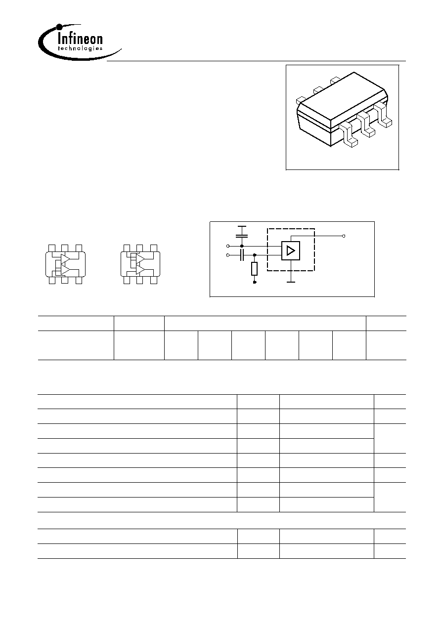
DUAL N-Channel MOSFET Tetrode
·
Low noise gain controlled input stages of UHF-
and VHF-tuners with 5V supply voltage
·
Two AGC amplifiers in one single package
·
Integrated gate protection diodes
·
Low noise figure
·
High gain, high forward transadmittance
·
Improved cross modulation at gain reduction
·
High AGC-range
BG3140
BG3140R
EHA07461
GND
G1
G2
Drain
AGC
HF
Input
HF Output
+ DC
GG
V
G1
R
A
B
4
5
6
1
2
3
1
2
3
4
5
6
A
B
ESD
: Electrostatic discharge sensitive device, observe handling precaution!
Type
Package
Pin Configuration
Marking
BG3140
BG3140R
SOT363
SOT363
1=G1
1=G1
2=G2
2=S
3=D
3=D
4=D
4=D
5=S
5=G2
6=G1
6=G1
KDs
KKs
180° rotated tape loading orientation available
Maximum Ratings
Parameter
Symbol
Value
Unit
Drain-source voltage
V
DS
8
V
Continuous drain current
I
D
25
mA
Gate 1/ gate 2-source current
±
I
G1/2SM
1
Gate 1/ gate 2-source voltage
±
V
G1/G2S
6
V
Total power dissipation, T
S
78°C
P
tot
160
mW
Storage temperature
T
stg
-55 ... 150
°C
Channel temperature
T
ch
150
Thermal Resistance
Parameter
Symbol
Value
Unit
Channel - soldering point
1)
R
thchs
280
K/W
1For calculation of R
thJA
please refer to Application Note Thermal Resistance

Feb-27-2004
2
BG3140...
Electrical Characteristics
Parameter
Symbol
Values
Unit
min.
typ.
max.
DC Characteristics
Drain-source breakdown voltage
I
D
= 10 µA, V
G1S
= 0 , V
G2S
= 0
V
(BR)DS
12
-
-
V
Gate1-source breakdown voltage
+I
G1S
= 10 mA, V
G2S
= 0 , V
DS
= 0
+V
(BR)G1SS
6
-
15
Gate2-source breakdown voltage
+I
G2S
= 10 mA, V
G1S
= 0 , V
DS
= 0
+V
(BR)G2SS
6
-
15
Gate1-source leakage current
V
G1S
= 6 V, V
G2S
= 0
+I
G1SS
-
-
50
µA
Gate2-source leakage current
V
G2S
= 8 V, V
G1S
= 0 , V
DS
= 0
+I
G2SS
-
-
50
nA
Drain current
V
DS
= 5 V, V
G1S
= 0 , V
G2S
= 4.5 V
I
DSS
-
-
10
µA
Drain-source current
V
DS
= 5 V, V
G2S
= 4 V, R
G1
= 70
k
I
DSX
-
15
-
mA
Gate1-source pinch-off voltage
V
DS
= 5 V, V
G2S
= 4 V, I
D
= 20 µA
V
G1S(p)
-
0.7
-
V
Gate2-source pinch-off voltage
V
DS
= 5 V, I
D
= 20 µA
V
G2S(p)
-
0.6
-
Feb-27-2004
3
BG3140...
Electrical Characteristics
Parameter
Symbol
Values
Unit
min.
typ.
max.
AC Characteristics - (verified by random sampling)
Forward transconductance
V
DS
= 5 V, V
G2S
= 4 V
g
fs
-
42
-
mS
Gate1 input capacitance
V
DS
= 5 V, V
G2S
= 4 V, f = 1 MHz
C
g1ss
-
1.9
-
pF
Output capacitance
V
DS
= 5 V, V
G2S
= 4 V, f = 100 MHz
C
dss
-
1.1
-
Power gain (self biased)
V
DS
= 5 V, I
D
= 10 mA, V
G2S
= 4 V,
f = 800 MHz
V
DS
= 5 V, I
D
= 10 mA, V
G2S
= 4 V,
f = 45 MHz
G
p
-
-
24
31
-
-
dB
Noise figure
V
DS
= 5 V, I
D
= 10 mA, V
G2S
= 4 V,
f = 800 MHz
V
DS
= 5 V, I
D
= 10 mA, V
G2S
= 4 V,
f = 45 MHz
F
-
-
1.3
1.7
-
-
dB
Gain control range
V
DS
= 5 V, V
G2S
= 4...0 V, f = 800 MHz
G
p
45
-
-
Cross-modulation k=1%, f
w
=50MHz, f
unw
=60MHz
AGC = 0 dB
AGC = 10 dB
AGC = 40 dB
X
mod
96
-
96
-
86
100
-
-
-
-