2005-10-14
1
BFR183F
3
1
2
NPN Silicon RF Transistor*
·
For low noise, high-gain broadband amplifiers at
collector currents from 2 mA to 30 mA
·
f
T
= 8 GHz, F = 0.9 dB at 900 MHz
* Short term description
ESD (Electrostatic discharge) sensitive device, observe handling precaution!
Type
Marking
Pin Configuration
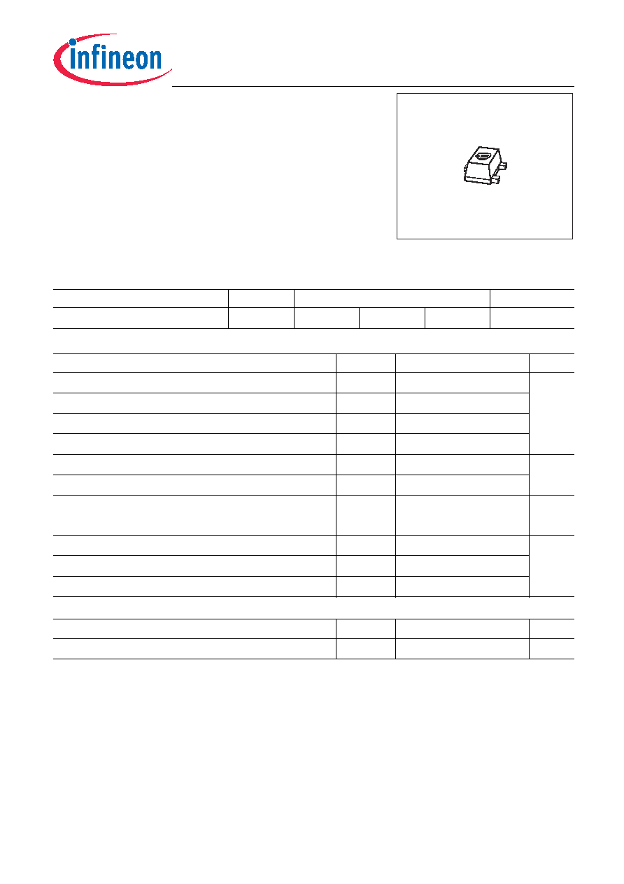
Package
BFR183F
RHs
1=B
2=E
3=C
TSFP-3
Maximum Ratings
Parameter
Symbol
Value
Unit
Collector-emitter voltage
V
CEO
12
V
Collector-emitter voltage
V
CES
20
Collector-base voltage
V
CBO
20
Emitter-base voltage
V
EBO
2
Collector current
I
C
65
mA
Base current
I
B
5
Total power dissipation
1)
T
S
62 °C
P
tot
450
mW
Junction temperature
T
j
150
°C
Ambient temperature
T
A
-65 ... 150
Storage temperature
T
stg
-65 ... 150
Thermal Resistance
Parameter
Symbol
Value
Unit
Junction - soldering point
2)
R
thJS
195
K/W
1
T
S
is measured on the collector lead at the soldering point to the pcb
2For calculation of R
thJA
please refer to Application Note Thermal Resistance

2005-10-14
2
BFR183F
Electrical Characteristics at T
A
= 25°C, unless otherwise specified
Parameter
Symbol
Values
Unit
min.
typ.
max.
DC Characteristics
Collector-emitter breakdown voltage
I
C
= 1 mA, I
B
= 0
V
(BR)CEO
12
-
-
V
Collector-emitter cutoff current
V
CE
= 20 V, V
BE
= 0
I
CES
-
-
100
µA
Collector-base cutoff current
V
CB
= 10 V, I
E
= 0
I
CBO
-
-
100
nA
Emitter-base cutoff current
V
EB
= 1 V, I
C
= 0
I
EBO
-
-
1
µA
DC current gain-
I
C
= 15 mA, V
CE
= 8 V, pulse measured
h
FE
70
100
140
-

2005-10-14
3
BFR183F
Electrical Characteristics at T
A
= 25°C, unless otherwise specified
Parameter
Symbol
Values
Unit
min.
typ.
max.
AC Characteristics (verified by random sampling)
Transition frequency
I
C
= 25 mA, V
CE
= 8 V, f = 500 MHz
f
T
6
8
-
GHz
Collector-base capacitance
V
CB
= 10 V, f = 1 MHz, V
BE
= 0 ,
emitter grounded
C
cb
-
0.34
0.54 pF
Collector emitter capacitance
V
CE
= 10 V, f = 1 MHz, V
BE
=
0, base
grounded
C
ce
-
0.2
-
Emitter-base capacitance
V
EB
= 0.5 V, f = 1 MHz, V
CB
= 0 ,
collector grounded
C
eb
-
1.1
-
Noise figure
I
C
= 5 mA, V
CE
= 8 V, Z
S
= Z
Sopt
,
f = 900 MHz
f = 1.8 GHz
F
-
-
0.9
1.4
-
-
dB
Power gain, maximum stableI
C
= 15 mA
I
C
= 15 mA, V
CE
= 8 V, Z
S
= Z
Sopt
, Z
L
= Z
Lopt
,
f = 900 MHz
G
ms
-
21
-
dB
Power gain, maximum available
1)
I
C
= 15 mA, V
CE
= 8 V, Z
S
= Z
Sopt
, Z
L
= Z
Lopt
,
f = 1.8 GHz
G
ma
-
14.5
-
dB
Transducer gain
I
C
= 15 mA, V
CE
= 8 V, Z
S
= Z
L
= 50
,
f = 900 MHz
f = 1.8 MHz
|S
21e
|
2
-
-
17
11
-
-
dB
Third order intercept point at output
2)
V
CE
= 8 V, I
C
= 15 mA, f
=
900MHz
,
Z
S
=Z
L
=50
IP
3
-
26
-
dBm
1dB Compression point
3)
I
C
= 15 mA, V
CE
= 8 V, f
=
900MHz
,
Z
S
=Z
L
=50
P
-1dB
-
10.5
-
1
G
ma
= |
S
21e
/
S
12e
| (k-(k˛-1)
1/2
),
G
ms = |
S
21 /
S
12|
2IP3 value depends on termination of all intermodulation frequency components.
Termination used for this measurement is 50
from 0.1 MHz to 6 GHz
3DC current at no input power
2005-10-14
4
BFR183F
SPICE Parameter (Gummel-Poon Model, Berkley-SPICE 2G.6 Syntax):
Transitor Chip Data:
NF =
0.80799
-
ISE =
16.818
fA
NR =
0.99543
-
ISC =
1.3559
fA
IRB =
0.43801
mA
RC =
0.20486
MJE =
0.45354
-
VTF =
0.50905
V
CJC =
460.11
fF
XCJC =
0.053823
-
VJS =
0.75
V
EG =
1.11
eV
TNOM
300
K
IS =
1.0345
fA
VAF =
14.772
V
NE =
1.2149
-
VAR =
3.4276
V
NC =
0.85331
-
RBM =
1.0112
CJE =
23.077
fF
TF =
22.746
ps
ITF =
1.8773
mA
VJC =
1.1967
V
TR =
1.0553
ns
MJS =
0
-
XTI =
3
-
BF =
115.98
-
IKF =
0.14562
A
BR =
10.016
-
IKR =
0.013483
A
RB =
2.5426
RE =
1.3435
-
VJE =
1.0792
V
XTF =
0.36823
-
PTF =
0
deg
MJC =
0.3
-
CJS =
0
fF
XTB =
0
-
FC =
0.54852
All parameters are ready to use, no scalling is necessary. Extracted on behalf of Infineon Technologies AG by:
Institut für Mobil- und Satellitentechnik (IMST)
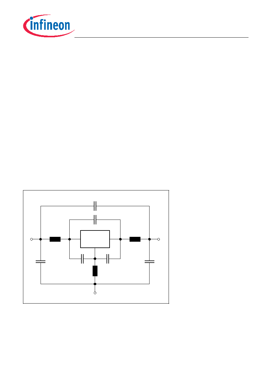
Package Equivalent Circuit:
L
1
=
0.556
nH
L
2
=
0.675
nH
L
3
=
0.381
nH
C
1
=
43
fF
C
2
=
123
fF
C
3
=
66
fF
C
4
=
10
fF
C
5
=
36
fF
C
6
=
47
fF
EHA07524
Transistor C'
L
E'
B'
3
4
C
C
Chip
E
L
1
5
C
B
2
L
C
6
C
1
C
2
C
3
For examples and ready to use parameters
please contact your local Infineon Technologies
distributor or sales office to obtain a Infineon
Technologies CD-ROM or see Internet:
http//www.infineon.com/silicondiscretes
Valid up to 6GHz
2005-10-14
5
BFR183F
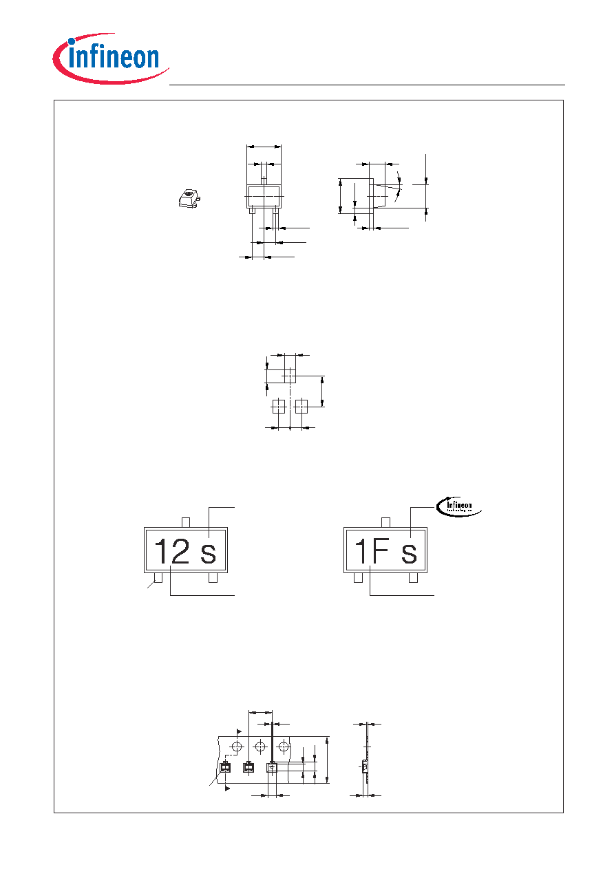
Package TSFP-3
4
P a c k a g e O u t l i n e
F o o t P r i n t
M a r k i n g L a y o u t
S t a n d a r d P a c k i n g
Reel ř180 mm = 3.000 Pieces/Reel
Reel ř330 mm = 10.000 Pieces/Reel
±0.05
0.2
3
±0.05
1.2
1
2
10° MAX.
±0.05
0.8
1.2
±0.05
±0.04
0.55
±0.05
0.2
±0.05
0.15
±0.05
0.2
0.4
±0.05
0.4
±0.05
0.4
0.45
1.05
0.4
0.4
Manufacturer
Type code
BCR847BF
Example
Pin 1
0.2
1.35
0.3
0.7
1.2
1.5
8
Pin 1

2005-10-14
6
BFR183F
Published by Infineon Technologies AG,
St.-Martin-Strasse 53,
81669 München
© Infineon Technologies AG 2005.
All Rights Reserved.
Attention please!
The information herein is given to describe certain components and shall not be
considered as a guarantee of characteristics.
Terms of delivery and rights to technical change reserved.
We hereby disclaim any and all warranties, including but not limited to warranties of
non-infringement, regarding circuits, descriptions and charts stated herein.
Information
For further information on technology, delivery terms and conditions and prices
please contact your nearest Infineon Technologies Office (www.Infineon.com).
Warnings
Due to technical requirements components may contain dangerous substances.
For information on the types in question please contact your nearest Infineon
Technologies Office.
Infineon Technologies Components may only be used in life-support devices or
systems with the express written approval of Infineon Technologies, if a failure of
such components can reasonably be expected to cause the failure of that life-support
device or system, or to affect the safety or effectiveness of that device or system.
Life support devices or systems are intended to be implanted in the human body, or
to support and/or maintain and sustain and/or protect human life. If they fail, it is
reasonable to assume that the health of the user or other persons may be endangered.