BC817UPN
Aug-21-2002
1
NPN/PNP Silicon Transistor Array
For AF input stages and driver applications
High current gain
Low collector-emitter saturation voltage
Two (galvanic) internal isolated NPN/PNP
Transistors in one package
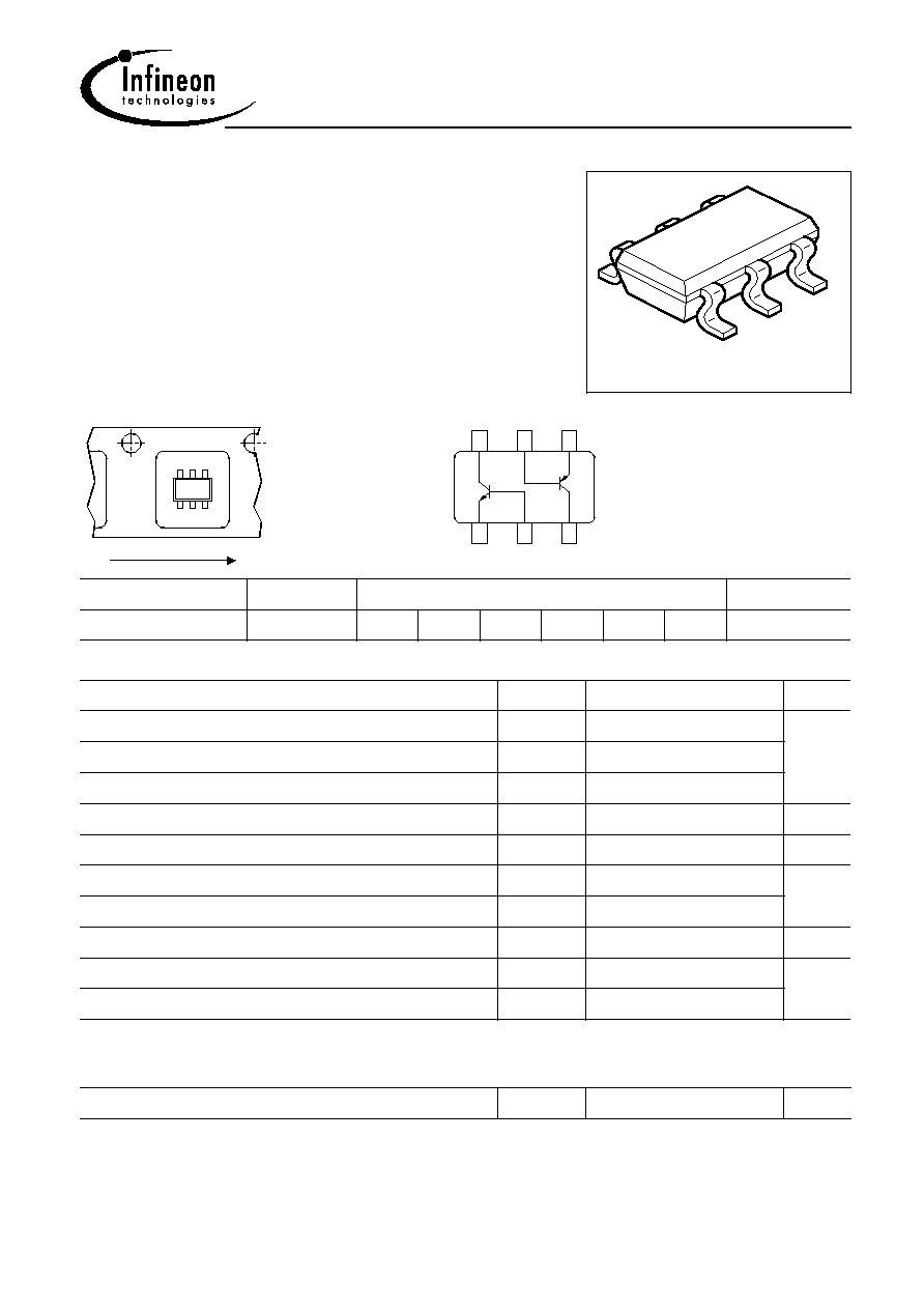
Tape loading orientation
VPW09197
1
2
3
4
5
6
SC74_Tape
1 2 3
4
5
6
W1s
Direction of Unreeling
Top View
Marking on SC74 package
(for example W1s)
corresponds to pin 1 of device
Position in tape: pin 1
opposite of feed hole side
EHA07177
6
5
4
3
2
1
C1
B2
E2
C2
B1
E1
TR1
TR2
Type
Marking
Pin Configuration
Package
BC817UPN
1Bs
1=E1 2=B1 3=C2 4=E2 5=B2 6=C1 SC74
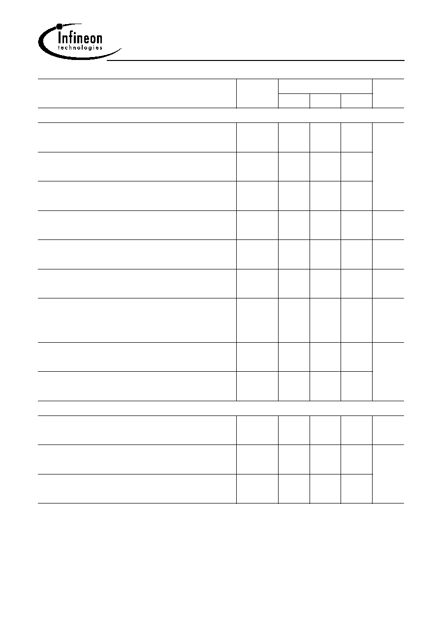
Maximum Ratings
Parameter
Symbol
Value
Unit
Collector-emitter voltage
V
CEO
45
V
Collector-base voltage
V
CBO
50
Emitter-base voltage
V
EBO
5
DC collector current
I
C
500
mA
Peak collector current
I
CM
1
A
Base current
I
B
100
mA
Peak base current
I
BM
200
Total power dissipation
,
T
S
= 115 °C
P
tot
330
mW
Junction temperature
T
j
150
°C
Storage temperature
T
stg
-65 ... 150
Thermal Resistance
Junction - soldering point
1)
R
thJS
105
K/W
1For calculation of R
thJA
please refer to Application Note Thermal Resistance
BC817UPN
Aug-21-2002
2
Electrical Characteristics at T
A
=25°C, unless otherwise specified
Parameter
Symbol
Values
Unit
min.
typ.
max.
DC Characteristics
Collector-emitter breakdown voltage
I
C
= 10 mA,
I
B
= 0
V
(BR)CEO
45
-
-
V
Collector-base breakdown voltage
I
C
= 10 µA,
I
E
= 0
V
(BR)CBO
50
-
-
Emitter-base breakdown voltage
I
E
= 10 µA,
I
C
= 0
V
(BR)EBO
5
-
-
Collector cutoff current
V
CB
= 25 V,
I
E
= 0
I
CBO
-
-
100
nA
Collector cutoff current
V
CB
= 25 V,
I
E
= 0 ,
T
A
= 150 °C
I
CBO
-
-
50
µA
Emitter cutoff current
V
EB
= 4 V,
I
C
= 0
I
EBO
-
-
100
nA
DC current gain 1)
I
C
= 100 mA,
V
CE
= 1 V
I
C
= 300 mA,
V
CE
= 1 V
h
FE
160
100
250
-
400
-
-
Collector-emitter saturation voltage1)
I
C
= 500 mA,
I
B
= 50 mA
V
CEsat
-
-
0.7
V
Base-emitter saturation voltage 1)
I
C
= 500 mA,
I
B
= 50 mA
V
BEsat
-
-
1.2
AC Characteristics
Transition frequency
I
C
= 50 mA,
V
CE
= 5 V,
f
= 100 MHz
f
T
-
170
-
MHz
Collector-base capacitance
V
CB
= 10 V,
f
= 1 MHz
C
cb
-
6
-
pF
Emitter-base capacitance
V
EB
= 0.5 V,
f
= 1 MHz
C
eb
-
60
-
1) Pulse test: t < 300
s; D < 2%

