COMMERCIAL TEMPERATURE RANGE
IDTCV110J
PROGRAMMABLE FLEXPC CLOCK FOR P4 PROCESSOR
1
MAY 2004
IDTCV110J
COMMERCIAL TEMPERATURE RANGE
PROGRAMMABLE FLEXPC
CLOCK FOR P4 PROCESSOR
XTAL
Osc Amp
SM Bus
Controller
Control
Logic
CPU CLK
Output Buffers
Stop Logic
X1
X2
SDATA
SCLK
V
TT_PWRGD
#/PD
FSA.B.C
I
REF
CPU[1:0]
REF
CPU_ITP/SRC7
PLL1
SSC
N Programmable
ITP_EN
SRC CLK
Output Buffer
Stop Logic
48MHz/96MHz
Output BUffer
I
REF
SRC[6:1]
48MHz
DOT96
PLL2
SSC
N Programmable
PLL3
PCI[5:0], PCIF[2:0]
The IDT logo is a registered trademark of Integrated Device Technology, Inc.
© 2004 Integrated Device Technology, Inc.
DSC-6507/12
FEATURES:
· One high precision PLL for CPU, SSC, and N programming
· One high precision PLL for SRC/PCI/SATA, SSC, and N
programming
· One high precision PLL for 96MHz/48MHz
· Band-gap circuit for differential outputs
· Support spread spectrum modulation, down spread 0.5%
· Support SMBus block read/write, index read/write
· Selectable output strength for REF
· Allows for CPU frequency to change to a higher frequency for
maximum system computing power
· Available in SSOP package
FUNCTIONAL BLOCK DIAGRAM
DESCRIPTION:
IDTCV110J is a 56 pin clock device. The CPU output buffer is designed to
support up to 400MHz processor. This chip has three PLLs inside for CPU/
SRC/PCI, SATA, and 48MHz/DOT96 IO clocks. One dedicated PLL for Serial
ATA clock provides high accuracy frequency. This device also implements
Band-gap referenced I
REF
to reduce the impact of V
DD
variation on differential
outputs, which can provide more robust system performance.
Static PLL frequency divide error can be as low as 36 ppm, worse case 114
ppm, providing high accuracy output clock. Each CPU/SRC/PCI, SATA clock
has its own Spread Spectrum selection, which allows for isolated changes
instead of affecting other clock groups.
OUTPUTS:
· 2*0.7V current mode differential CPU CLK pair
· 6*0.7V current mode differential SRC CLK pair, one dedicated
for SATA
· One CPU_ITP/SRC selectable CLK pair
· 9*PCI, 3 free running, 33.3MHz
· 1*96MHz, 1*48MHz
· 1*REF
KEY SPECIFICATION:
· CPU/SRC CLK cycle to cycle jitter < 85ps
· SATA CLK cycle to cycle jitter < 85ps
· PCI CLK cycle to cycle jitter < 250ps
· Static PLL frequency divide error < 114 ppm
· Static PLL frequency divide error for 48MHz < 5 ppm
COMMERCIAL TEMPERATURE RANGE
2
IDTCV110J
PROGRAMMABLE FLEXPC CLOCK FOR P4 PROCESSOR
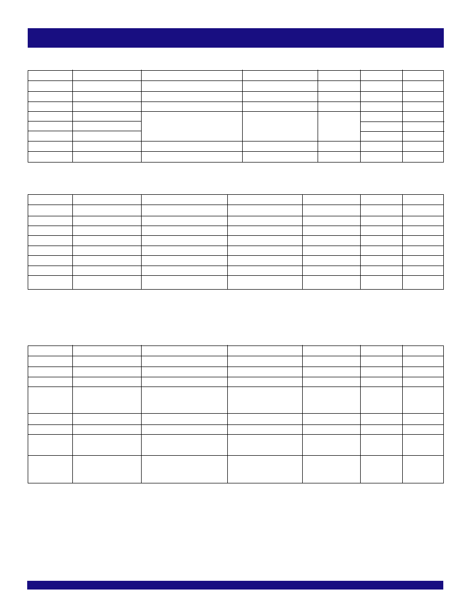
PIN CONFIGURATION
Symbol
Description
Min
Max
Unit
V
DDA
3.3V Core Supply Voltage
4.6
V
V
DDIN
3.3V Logic Input Supply Voltage GND - 0.5
4.6
V
T
STG
Storage Temperature
65
+150
°C
T
AMBIENT
Ambient Operating Temperature
0
+70
°C
T
CASE
Case Temperature
+115
°C
ESD Prot
Input ESD Protection
2000
V
Human Body Model
ABSOLUTE MAXIMUM RATINGS
(1)
NOTE:
1. Stresses greater than those listed under ABSOLUTE MAXIMUM RATINGS may cause
permanent damage to the device. This is a stress rating only and functional operation
of the device at these or any other conditions above those indicated in the operational
sections of this specification is not implied. Exposure to absolute maximum rating
conditions for extended periods may affect reliability.
SSOP
TOP VIEW
56
55
54
53
52
51
50
49
48
47
46
45
44
43
42
41
40
39
38
37
36
35
34
33
32
31
30
29
PCI2
PCI1
PCI0
FSC/TEST_SEL
REF
V
SS
_REF
XTAL_IN
XTAL_OUT
V
DD
_REF
SDA
SCL
V
SS
_CPU
CPU0
CPU0#
V
DD
_CPU
CPU1
CPU1#
I
REF
V
SSA
V
DDA
CPU2_ITP/SRC7
CPU2_ITP#/SRC7#
V
DD
_SRC
SRC6#
SRC5
SRC5#
V
SS
_SRC
1
2
3
4
5
6
7
8
9
10
11
12
13
14
15
16
17
18
19
20
21
22
23
24
25
26
27
28
V
DD
_PCI
V
SS
_PCI
PCI3
PCI4
PCI5
V
SS
_PCI
V
DD
_PCI
PCIF
0
/ITP
_
EN
PCIF1
V
TT
_P
WRGD#
/
PD
V
DD
48
USB48
V
SS
48
DOT96
DOT96#
FSB/TEST_MODE
PCIF2
FSA
SRC1
SRC1#
V
DD
_SRC
SRC2
SRC2#
SRC3
SRC3#
SRC4
SRC4#
V
DD
_SRC
SRC6
FREQUENCY SELECTION TABLE
FSC, B, A
CPU
SRC[7:1]
PCI
USB
DOT
REF
101
100
100
33.3
48
96
14.318
001
133
100
33.3
48
96
14.318
011
166
100
33.3
48
96
14.318
010
200
100
33.3
48
96
14.318
000
266
100
33.3
48
96
14.318
100
333
100
33.3
48
96
14.318
110
400
100
33.3
48
96
14.318
111
Reserve
100
33.3
48
96
14.318

COMMERCIAL TEMPERATURE RANGE
IDTCV110J
PROGRAMMABLE FLEXPC CLOCK FOR P4 PROCESSOR
3
PIN DESCRIPTION
Pin Number
Name
Type
Description
1
V
DD
_PCI
PWR
3.3V
2
V
SS
_PCI
GND
GND
3
PCI3
OUT
PCI clock
4
PCI4
OUT
PCI clock
5
PCI5
OUT
PCI clock
6
V
SS
_PCI
GND
GND
7
V
DD
_PCI
PWR
3.3V
8
PCIF0/ITP_EN
I/O
PCI clock, free running. CPU2 select (sampled on V
TT
_P
WRGD
# assertion) HIGH = CPU2.
9
PCIF1
OUT
PCI clock, free running
10
PCIF2
OUT
PCI clock, free running
11
V
DD
48
PWR
3.3V
12
USB48
OUT
48MHz clock
13
V
SS
48
GND
GND
14
DOT96
OUT
96MHz 0.7 current mode differential clock output
15
DOT96#
OUT
96MHz 0.7 current mode differential clock output
16
FSB/TEST_MODE
IN
CPU frequency selection. Selects R
EF
/N or Hi-Z when in test mode, Hi-Z = 1, R
EF
/N = 0.
17
V
TT
_P
WRGD
#/PD
IN
Level-sensitive strobe used to latch the FSA, FSB, FSC/TEST_SEL, and PCIF0/ITP_EN inputs. After
V
TT
_P
WRGD
# assertion, becomes a real-time input for asserting power down. (Active HIGH)
18
FSA
IN
CPU frequency selection
19
SRC1
OUT
Differential serial reference clock
20
SRC1#
OUT
Differential serial reference clock
21
V
DD
_SRC
PWR
3.3V
22
SRC2
OUT
Differential serial reference clock
23
SRC2#
OUT
Differential serial reference clock
24
SRC3
OUT
Differential serial reference clock
25
SRC3#
OUT
Differential serial reference clock
26
SRC4
OUT
Differential serial reference clock
27
SRC4#
OUT
Differential serial reference clock
28
V
DD
_SRC
PWR
3.3V
29
V
SS
_SRC
GND
GND
30
SRC5#
OUT
Differential serial reference clock
31
SRC5
OUT
Differential serial reference clock
32
SRC6#
OUT
Differential serial reference clock
33
SRC6
OUT
Differential serial reference clock
34
V
DD
_SRC
PWR
3.3V
35
CPU2_ITP#/SRC7#
OUT
Selectable CPU or SRC differential clock output. ITP_EN = 0 at V
TT
_P
WRGD
# assertion = SRC7#.
36
CPU2_ITP/SRC7
OUT
Selectable CPU or SRC differential clock output. ITP_EN = 0 at V
TT
_P
WRGD
# assertion = SRC7.
37
V
DDA
PWR
3.3V
38
V
SSA
GND
GND
39
I
REF
OUT
Reference current for differential output buffer
40
CPU1#
OUT
Host 0.7 current mode differential clock output
41
CPU1
OUT
Host 0.7 current mode differential clock output
42
V
DD
_CPU
PWR
3.3V
COMMERCIAL TEMPERATURE RANGE
4
IDTCV110J
PROGRAMMABLE FLEXPC CLOCK FOR P4 PROCESSOR
PIN DESCRIPTION (CONT.)
Pin Number
Name
Type
Description
43
CPU0#
OUT
Host 0.7 current mode differential clock output
44
CPU0
OUT
Host 0.7 current mode differential clock output
45
V
SS
_CPU
GND
GND
46
SCL
IN
SM Bus clock
47
SDA
I/O
SM Bus data
48
V
DD
_REF
PWR
3.3V
49
XTAL_OUT
OUT
XTAL output
50
XTAL_IN
IN
XTAL input
51
V
SS
_REF
GND
GND
52
REF
OUT
14.318 MHz reference clock output
53
FSC/TEST_SEL
IN
CPU frequency selection. Selects test mode if pulled to above 2V when V
TT
_P
WRGD
# is asserted LOW.
54
PCI0
OUT
PCI clock
55
PCI1
OUT
PCI clock
56
PCI2
OUT
PCI clock
INDEX BLOCK WRITE PROTOCOL
Bit
# of bits
From
Description
1
1
Master
Start
2-9
8
Master
D2h
10
1
Slave
Ack (Acknowledge)
11-18
8
Master
Register offset byte (starting byte)
19
1
Slave
Ack (Acknowledge)
20-27
8
Master
Byte count, N (0 is not valid)
28
1
Slave
Ack (Acknowledge)
29-36
8
Master
first data byte (Offset data byte)
37
1
Slave
Ack (Acknowledge)
38-45
8
Master
2nd data byte
46
1
Slave
Ack (Acknowledge)
:
Master
Nth data byte
Slave
Acknowledge
Master
Stop
INDEX BLOCK READ PROTOCOL
Master can stop reading any time by issuing the stop bit without waiting
until Nth byte (byte count bit30-37).
Bit
# of bits
From
Description
1
1
Master
Start
2-9
8
Master
D2h
10
1
Slave
Ack (Acknowledge)
11-18
8
Master
Register offset byte (starting byte)
19
1
Slave
Ack (Acknowledge)
20
1
Master
Repeated Start
21-28
8
Master
D3h
29
1
Slave
Ack (Acknowledge)
30-37
8
Slave
Byte count, N (block read back of N
bytes), power on is 8
38
1
Master
Ack (Acknowledge)
39-46
8
Slave
first data byte (Offset data byte)
47
1
Master
Ack (Acknowledge)
48-55
8
Slave
2nd data byte
Ack (Acknowledge)
:
Master
Ack (Acknowledge)
Slave
Nth data byte
Not acknowledge
Master
Stop
INDEX BYTE WRITE
Setting bit[11:18] = starting address, bit[20:27] = 01h.
INDEX BYTE READ
Setting bit[11:18] = starting address. After reading back the first data byte,
master issues Stop bit.
COMMERCIAL TEMPERATURE RANGE
IDTCV110J
PROGRAMMABLE FLEXPC CLOCK FOR P4 PROCESSOR
5
CONTROL REGISTERS
N PROGRAMMING PROCEDURE
·
Use Index byte write.
·
For N programming, the user only needs to access Byte17, Byte 25, and Byte8.
1.
Write Byte17 for CPU PLL N, CPU f = N* Resolution, see resolution table below Byte17.
2.
Write Byte25 for SRC PLL N, SRC f = N*0.666667, PCI = SRC f /3, SATA f = SRC f.
3.
Enable N Programming bit, Byte8 bit1. Once this bit is enabled, any N value will be changed on the fly.
·
Center spread only works when the N Programming bit is enabled. Down spread is OK even N Programming bit is disabled
·
It is OK to change N value to any value on the bench test board. In the system, IDT recommends the stepping change. It is unknown how much
the system can sustain for each stepping change; the estimate is about 5. If the N changes too much in one step, the system will likely hang.
·
Note that SATA is with SRC PLL. This SATA Hard Drive might not operate during SRC N programming.
Most of the Bytes, from Byte8-Byte31, are used to adjust output waveforms and SSC modulation profiles. The power on setting will be changed according
to each power on frequency selection. To avoid mistakes, don't write on those byte (be careful about Block Write). It is suggested to use the Index Byte
write to access bytes.
SSC MAGNITUDE CONTROL, SMC
SMC[2:0]
000
-0.25
001
-0.5
010
-0.75
011
-1
100
±0.125
101
±0.25
110
±0.375
111
±0.5
FS_C, B, A
CPU
101
100
001
133
011
166
010
200
000
266
100
333
110
400
111
RESERVE
FREQUENCY SELECTION TABLE
RESOLUTION
CPU (MHz)
Resolution
N =
100
0.666667
150
133
0.666667
200
166
1.333333
125
200
1.333333
150
266
1.333333
200
333
2.666667
125
400
2.666667
150
COMMERCIAL TEMPERATURE RANGE
6
IDTCV110J
PROGRAMMABLE FLEXPC CLOCK FOR P4 PROCESSOR
BYTE 0
Bit
Output(s) Affected
Description/Function
0
1
Type
Power On
0
Reserved
1
SRC1, SRC1#
Output Enable
Tristate
Enable
RW
1
2
SRC2, SRC2#
Output Enable
Tristate
Enable
RW
1
3
SRC3, SRC3#
Output Enable
Tristate
Enable
RW
1
4
SRC4, SRC4#
Output Enable
Tristate
Enable
RW
1
5
SRC5, SRC5#
Output Enable
Tristate
Enable
RW
1
6
SRC6, SRC6#
Output Enable
Tristate
Enable
RW
1
7
CPU2, CPU2#/
Output Enable
Tristate
Enable
RW
1
SRC7, SRC7#
BYTE 1
Bit
Output(s) Affected
Description/Function
0
1
Type
Power On
0
CPU[2:0], SRC[7:1],
Spread Spectrum mode enable
Spread off
Spread on
RW
0
PCI[5:0], PCIF[2:0]
1
CPU0, CPU0#
Output Enable
Tristate
Enable
RW
1
2
CPU1, CPU1#
Output Enable
Tristate
Enable
RW
1
3
Reserve
0
4
REF
Output Enable
Tristate
Enable
RW
1
5
USB48
Output Enable
Tristate
Enable
RW
1
6
DOT96
Output Enable
Tristate
Enable
RW
1
7
PCIF0
Output Enable
Tristate
Enable
RW
1
BYTE 2
Bit
Output(s) Affected
Description/Function
0
1
Type
Power On
0
PCIF1
Output Enable
Tristate
Enable
RW
1
1
PCIF2
Output Enable
Tristate
Enable
RW
1
2
PCI0
Output Enable
Tristate
Enable
RW
1
3
PCI1
Output Enable
Tristate
Enable
RW
1
4
PCI2
Output Enable
Tristate
Enable
RW
1
5
PCI3
Output Enable
Tristate
Enable
RW
1
6
PCI4
Output Enable
Tristate
Enable
RW
1
7
PCI5
Output Enable
Tristate
Enable
RW
1
BYTE 3
Bit
Output(s) Affected
Description / Function
0
1
Type
Power On
0
Reserved
1
SRC1
RW
0
2
SRC2
RW
0
3
SRC3
Allow controlled by software
Free running, not
Stopped with
RW
0
4
SRC4
PCI_STOP, byte 6, bit 3, assertion
affected by PCI_STOP
PCI_STOP
RW
0
5
SRC5
RW
0
6
SRC6
RW
0
7
SRC7
RW
0
COMMERCIAL TEMPERATURE RANGE
IDTCV110J
PROGRAMMABLE FLEXPC CLOCK FOR P4 PROCESSOR
7
BYTE 4
Bit
Output(s) Affected
Description / Function
0
1
Type
Power On
0
Reserved
RW
1
1
Reserved
RW
1
2
Reserved
RW
1
3
PCIF0
RW
0
4
PCIF1
Allow controlled by software
Not stopped
Stopped with
RW
0
5
PCIF2
PCI_STOP, byte 6, bit 3, assertion
by PCI_STOP
PCI_STOP
RW
0
6
DOT96
DOT96 power down drive mode
Driven in power down
Tristate
RW
0
7
Reserved
0
BYTE 5
Bit
Output(s) Affected
Description / Function
0
1
Type
Power On
0
CPU0, CPU0#
CPU0 P
WRDWN
drive mode
Driven in power down
Tristate in power down
RW
0
1
CPU1, CPU1#
CPU1 P
WRDWN
drive mode
Driven in power down
Tristate in power down
RW
0
2
CPU2, CPU2#
CPU2 P
WRDWN
drive mode
Driven in power down
Tristate in power down
RW
0
3
SRC[7:1], SRC[7:1]#
SRC P
WRDWN
drive mode
Driven in power down
Tristate in power down
RW
0
4
Reserved
0
5
Reserved
0
6
Reserved
0
7
SRC[7:1], SRC[7:1]#
SRC PCI_STOP drive mode
Driven in PCI_STOP
Tristate when stopped
RW
0
BYTE 6
Bit
Output(s) Affected
Description / Function
0
1
Type
Power On
0
CPU[2:0]
FSA latched value on power up
R
1
CPU[2:0]
FSB latched value on power up
R
2
CPU[2:0]
FSC latched value on power up
R
3
PCI, SRC
Software PCI_STOP control for
Stop all PCI, PCIF, and
Software STOP
RW
1
PCI and SRC CLK
SRC which can be stopped
Disabled
by PCI_STOP#
4
REF
REF drive strength
1x drive
2x drive
1
5
Reserved
0
6
Test clock mode entry control
Normal operation
Test mode, controlled
RW
0
by Byte 6, Bit 7
7
CPU, SRC, PCI
Only valid when Byte 6, Bit 7
Hi-Z
REF/N
0
PCIF, REF,
is HIGH
USB48, DOT96
COMMERCIAL TEMPERATURE RANGE
8
IDTCV110J
PROGRAMMABLE FLEXPC CLOCK FOR P4 PROCESSOR
BYTE 7
Bit
Output(s) Affected
Description / Function
0
1
Type
Power On
0
Vendor ID
R
1
1
Vendor ID
R
0
2
Vendor ID
R
1
3
Vendor ID
R
0
4
Revision ID
R
0
5
Revision ID
R
0
6
Revision ID
R
0
7
Revision ID
R
0
BYTE 9
Bit
Output(s) Affected
Description / Function
0
1
Type
Power On
0
SRC SMC0
SRC/PCI SSC control
RW
1
1
SRC SMC1
see SMC table
RW
0
2
SRC SMC2
RW
0
3
Reserved
RW
0
4
CPU SMC0
CPU PLL SSC control
RW
1
5
CPU SMC1
see SMC table
RW
0
6
CPU SMC2
RW
0
7
Must be 0
Must be 0
RW
0
(Must be 0)
BYTE 8
Bit
Output(s) Affected
Description / Function
0
1
Type
Power On
0
One cycle read
Disable
Enable
RW
0
1
N Programming enable
Disable
Enable
RW
0
2
Reserved
RW
0
3
USB48
USB 48 Strength control
1x
2x
RW
0
4
USB PLL power down
Normal
Power down
RW
0
5
SRC PLL power down
Normal
Power down
RW
0
6
CPU PLL power down
Normal
Power down
RW
0
7
SRC, PLL2, SSC enable Only valid when Byte1 bit0 is 1
Disable
Enable
RW
1
BYTE 17
Bit
Output(s) Affected
Description / Function
0
1
Type
Power On
0
CPU_N0, LSB
CPU CLK = N* Resolution
RW
1
CPU_N1
see Resolution table
RW
2
CPU_N2
RW
3
CPU_N3
RW
4
CPU_N4
RW
5
CPU_N5
RW
6
CPU_N6
RW
7
CPU_N7, MSB
RW

COMMERCIAL TEMPERATURE RANGE
IDTCV110J
PROGRAMMABLE FLEXPC CLOCK FOR P4 PROCESSOR
9
BYTE 25
Bit
Output(s) Affected
Description / Function
0
1
Type
Power On
0
SRC_N0, LSB
SRC f = N*SRC Resolution
RW
1
SRC_N1
Resolution = 0.666667
RW
2
SRC_N2
100MHz N= 150
RW
3
SRC_N3
RW
4
SRC_N4
RW
5
SRC_N5
RW
6
SRC_N6
RW
7
SRC_N7, MSB
RW
BYTES 10-16: OUTPUT WAVEFORM ADJUSTMENT. DON'T WRITE OVER.
BYTES 18-24: OUTPUT WAVEFORM ADJUSTMENT. DON'T WRITE OVER.
BYTES 26-31: OUTPUT WAVEFORM ADJUSTMENT. DON'T WRITE OVER.
COMMERCIAL TEMPERATURE RANGE
10
IDTCV110J
PROGRAMMABLE FLEXPC CLOCK FOR P4 PROCESSOR
Symbol
Parameter
Test Conditions
Min.
Typ.
Max.
Unit
V
IH
Input HIGH Voltage
3.3V ± 5%
2
--
V
DD
+ 0.3
V
V
IL
Input LOW Voltage
3.3V ± 5%
V
SS
- 0.3
--
0.8
V
V
IH
_FS
LOW Voltage, HIGH Threshold
For FSA.B.C test_mode
0.7
--
V
DD
+ 0.3
V
V
IL
_FS
LOW Voltage, LOW Threshold
For FSA.B.C test_mode
V
SS
- 0.3
--
0.35
V
I
IL
Input LeakageCurrent
0< V
IN
< V
DD
, no internal pull-up or pull-down
5
--
+5
mA
I
DD3.3OP
Operating Supply Current
Full active, C
L
= full load
--
--
400
mA
I
DD3.3PD
Powerdown Current
All differential pairs driven
--
--
70
mA
All differential pairs tri-stated
--
--
12
F
I
Input Frequency
(1)
V
DD
= 3.3V
--
14.31818
--
MHz
L
PIN
Pin Inductance
(2)
--
--
7
nH
C
IN
Logic inputs
--
--
5
C
OUT
Input Capacitance
(2)
Output pin capacitance
--
--
6
pF
C
INX
X1 and X2 pins
--
--
5
T
STAB
Clock Stabilization
(2,3)
From V
DD
power-up or de-assertion of PD to first clock
--
--
1.8
ms
Modulation Frequency
(2)
Triangular modulation
30
--
33
KHz
T
DRIVE
_PD
(2)
CPU output enable after PD de-assertion
--
--
300
us
T
FALL
_PD
(2)
Fall time of PD
--
--
5
ns
T
RISE
_PD
(3)
Rise time of PD
--
--
5
ns
ELECTRICAL CHARACTERISTICS - INPUT / SUPPLY / COMMON OUTPUT
PARAMETERS
Following Conditions Apply Unless Otherwise Specified:
Operating Condition: T
A
= 0°C to +70°C, Supply Voltage: V
DD
= 3.3V ± 5%
NOTES:
1. Input frequency should be measured at the REF output pin and tuned to ideal 14.31818MHz to meet ppm frequency accuracy on PLL outputs.
2. This parameter is guaranteed by design, but not 100% production tested.
3. See TIMING DIAGRAMS for timing requirements.
COMMERCIAL TEMPERATURE RANGE
IDTCV110J
PROGRAMMABLE FLEXPC CLOCK FOR P4 PROCESSOR
11
Symbol
Parameter
Test Conditions
Min.
Typ.
Max.
Unit
Z
O
Current Source Output Impedance
(2)
V
O
= V
X
3000
--
--
V
OH3
Output HIGH Voltage
I
OH
= -1mA
2.4
--
--
V
V
OL3
Output LOW Voltage
I
OL
= 1mA
--
--
0.4
V
V
HIGH
Voltage HIGH
(2)
Statistical measurement on single-ended signal using
660
--
850
mV
V
LOW
Voltage LOW
(2)
oscilloscope math function
150
--
150
V
OVS
Max Voltage
(2)
Measurement on single-ended signal using absolute value
--
--
1150
mV
V
UDS
Min Voltage
(2)
300
--
--
V
CROSS(ABS)
Crossing Voltage (abs)
(2)
250
--
550
mV
d - V
CROSS
Crossing Voltage (var)
(2)
Variation of crossing over all edges
--
--
140
mV
ppm
Long Accuracy
(2,3)
See T
PERIOD
Min. - Max. values
300
--
300
ppm
400MHz nominal/spread
2.4993
--
2.5008
333.33MHz nominal/spread
2.9991
--
3.0009
266.66MHz nominal/spread
3.7489
--
3.7511
T
PERIOD
Average Period
(3)
200MHz nominal/spread
4.9985
--
5.0015
ns
166.66MHz nominal/spread
5.9982
--
6.0018
133.33MHz nominal/spread
7.4978
--
7.5023
100MHz nominal/spread
9.997
--
10.003
96MHz nominal
10.4135
--
10.4198
400MHz nominal/spread
2.4143
--
--
333.33MHz nominal/spread
2.9141
--
--
266.66MHz nominal/spread
3.6639
--
--
200MHz nominal/spread
4.9135
--
--
T
ABSMIN
Absolute Min Period
(2,3)
166.66MHz nominal/spread
5.9132
--
--
ns
133.33MHz nominal/spread
7.4128
--
--
100MHz nominal/spread
9.912
--
--
96MHz nominal
10.1635
--
--
t
R
Rise Time
(2)
V
OL
= 0.175V, V
OH
= 0.525V
175
--
700
ps
t
F
Fall Time
(2)
V
OL
= 0.175V, V
OH
= 0.525V
175
--
700
ps
d-t
R
Rise Time Variation
(2)
--
--
125
ps
d-t
F
Fall Time Variation
(2)
--
--
125
ps
d
T3
Duty Cycle
(2)
Measurement from differential waveform
45
--
55
%
t
SK
3
Skew
(2)
V
T
= 50%
--
--
100
ps
t
JCYC
-
CYC
Jitter, Cycle to Cycle
(2)
Measurement from differential waveform
--
--
85
ps
ELECTRICAL CHARACTERISTICS - CPU, SRC, AND DOT96 0.7 CURRENT MODE
DIFFERENTIAL PAIR
(1)
Following Conditions Apply Unless Otherwise Specified:
Operating Condition: T
A
= 0°C to +70°C, Supply Voltage: V
DD
= 3.3V ± 5%; C
L
= 2pF
NOTES:
1. SRC clock outputs run only at 100MHz or 200MHz. Specs for 133.33 and 166.66 do not apply to SRC clock pair.
2. This parameter is guaranteed by design, but not 100% production tested.
3. All long term accuracy and clock period specifications are guaranteed with the assumption that the REF output is at 14.31818MHz.

COMMERCIAL TEMPERATURE RANGE
12
IDTCV110J
PROGRAMMABLE FLEXPC CLOCK FOR P4 PROCESSOR
Symbol
Parameter
Test Conditions
Min.
Typ.
Max.
Unit
ppm
Long Accuracy
(1,2)
See Tperiod Min. - Max. values
--
--
300
ppm
T
PERIOD
Clock Period
(2)
33.33MHz output nominal
29.991
--
30.009
ns
33.33MHz output spread
29.991
--
30.1598
V
OH
Output HIGH Voltage
I
OH
= -1mA
2.4
--
--
V
V
OL
Output LOW Voltage
I
OL
= 1mA
--
--
0.55
V
I
OH
Output HIGH Current
V
OH
at Min. = 1V
-33
--
--
mA
V
OH
at Max. = 3.135V
--
--
-33
I
OL
Output LOW Current
V
OL
at Min. = 1.95V
30
--
--
mA
V
OL
at Max. = 0.4V
--
--
38
Edge Rate
(1)
Rising edge rate
1
--
4
V/ns
Edge Rate
(1)
Falling edge rate
1
--
4
V/ns
t
R1
Rise Time
(1)
V
OL
= 0.4V, V
OH
= 2.4V
0.5
--
2
ns
t
F1
Fall Time
(1)
V
OL
= 0.4V, V
OH
= 2.4V
0.5
--
2
ns
d
T1
Duty Cycle
(1)
V
T
= 1.5V
45
--
55
%
t
SK1
Skew
(1)
V
T
= 1.5V
--
--
500
ps
t
JCYC
-
CYC
Jitter
(1)
V
T
= 1.5V
--
--
250
ps
ELECTRICAL CHARACTERISTICS - PCICLK / PCICLK_F
Following Conditions Apply Unless Otherwise Specified:
Operating Condition: T
A
= 0°C to +70°C, Supply Voltage: V
DD
= 3.3V ± 5%; C
L
= 10 - 30pF
NOTES:
1. This parameter is guaranteed by design, but not 100% production tested.
2. All long term accuracy and clock period specifications are guaranteed with the assumption that the REF output is at 14.31818MHz.
Symbol
Parameter
Test Conditions
Min.
Typ.
Max.
Unit
ppm
Long Accuracy
(1,2)
See Tperiod Min. - Max. values
--
--
300
ppm
T
PERIOD
Clock Period
(2)
48MHz output nominal
20.8257
--
20.834
ns
V
OH
Output HIGH Voltage
I
OH
= -1mA
2.4
--
--
V
V
OL
Output LOW Voltage
I
OL
= 1mA
--
--
0.55
V
I
OH
Output HIGH Current
V
OH
at Min. = 1V
-29
--
--
mA
V
OH
at Max. = 3.135V
--
--
-23
I
OL
Output LOW Current
V
OL
at Min. = 1.95V
29
--
--
mA
V
OL
at Max. = 0.4V
--
--
27
Edge Rate
(1)
Rising edge rate
1
--
2
V/ns
Edge Rate
(1)
Falling edge rate
1
--
2
V/ns
t
R1
Rise Time
(1)
V
OL
= 0.4V, V
OH
= 2.4V
1
--
2
ns
t
F1
Fall Time
(1)
V
OL
= 0.4V, V
OH
= 2.4V
1
--
2
ns
d
T1
Duty Cycle
(1)
V
T
= 1.5V
45
--
55
%
ELECTRICAL CHARACTERISTICS, 48MHZ, USB
Following Conditions Apply Unless Otherwise Specified:
Operating Condition: T
A
= 0°C to +70°C, Supply Voltage: V
DD
= 3.3V ± 5%; C
L
= 10 - 20pF
NOTES:
1. This parameter is guaranteed by design, but not 100% production tested.
2. All long term accuracy and clock period specifications are guaranteed with the assumption that the REF output is at 14.31818MHz.

COMMERCIAL TEMPERATURE RANGE
IDTCV110J
PROGRAMMABLE FLEXPC CLOCK FOR P4 PROCESSOR
13
Symbol
Parameter
Test Conditions
Min.
Typ.
Max.
Unit
ppm
Long Accuracy
(1)
See Tperiod Min. - Max. values
--
--
300
ppm
T
PERIOD
Clock Period
14.318MHz output nominal
69.827
--
69.855
ns
V
OH
Output HIGH Voltage
(1)
I
OH
= -1mA
2.4
--
--
V
V
OL
Output LOW Voltage
(1)
I
OL
= 1mA
--
--
0.4
V
I
OH
Output HIGH Current
(1)
V
OH
at Min. = 1V, V
OH
at Max. = 3.135V
-33
--
-33
mA
I
OL
Output LOW Current
(1)
V
OL
at Min. = 1.95V, V
OL
at Max. = 0.4V
30
--
38
mA
t
R1
Rise Time
(1)
V
OL
= 0.4V, V
OH
= 2.4V
1
--
2
ns
t
F1
Fall Time
(1)
V
OL
= 0.4V, V
OH
= 2.4V
1
--
2
ns
t
SK1
Skew
(1)
V
T
= 1.5V
--
--
500
ps
d
T1
Duty Cycle
(1)
V
T
= 1.5V
45
--
55
%
t
JCYC
-
CYC
Jitter
(1)
V
T
= 1.5V
--
--
1000
ps
ELECTRICAL CHARACTERISTICS - REF-14.318MHZ
Following Conditions Apply Unless Otherwise Specified:
Operating Condition: T
A
= 0°C to +70°C, Supply Voltage: V
DD
= 3.3V ± 5%; C
L
= 10 - 20pF
NOTE:
1. This parameter is guaranteed by design, but not 100% production tested.
PCI STOP FUNCTIONALITY
If PCIF (2:0) and SRC clocks are set to be free-running through SMBus programming, they will ignore the PCI_STOP register bit.
PCI_STOP
CPU
CPU#
SRC
SRC#
PCIF/PCI
USB
DOT96
DOT96#
REF
(Byte 6 bit 3)
1
Normal
Normal
Normal
Normal
33MHz
48MHz
Normal
Normal
14.318MHz
0
Normal
Normal
I
REF
* 6 or float
Low
Low
48MHz
Normal
Normal
14.318MHz
COMMERCIAL TEMPERATURE RANGE
14
IDTCV110J
PROGRAMMABLE FLEXPC CLOCK FOR P4 PROCESSOR
PD, POWER DOWN
PD is an asynchronous active high input used to shut off all clocks cleanly prior to clock power. When PD is asserted high all clocks will be driven low before
turning off the VCO. In PD de-assertion all clocks will start without glitches.
PD ASSERTION
PD
CPU 133MHz
CPU# 133MHz
SRC 100MHz
SRC# 100MHz
USB 48MHz
PCI 33MHz
REF 14.31818
PD
CPU
CPU#
SRC
SRC#
PCIF/PCI
USB
DOT96
DOT96#
REF
0
Normal
Normal
Normal
Normal
33MHz
48MHz
Normal
Normal
14.318MHz
1
I
REF
* 2 or float
Float
I
REF
* 2 or float
Float
Low
Low
I
REF
* 2 or float
Float
Low
COMMERCIAL TEMPERATURE RANGE
IDTCV110J
PROGRAMMABLE FLEXPC CLOCK FOR P4 PROCESSOR
15
PD DE-ASSERTION
The time from the de-assertion of PD or until power supply ramps to get stable clocks will be less than 1.8ms. If the drive mode control bit for PD tristate is
programmed to `1' the stopped differential pair must first be driven high to a minimum of 200mV in less than 300µs of PD deassertion.
PD
CPU 133MHz
CPU# 133MHz
SRC 100MHz
SRC# 100MHz
USB 48MHz
PCI 33MHz
REF 14.31818
t
STABLE
<1.8mS
t
DRIVE_PD
<300
µ
S, <200mV

COMMERCIAL TEMPERATURE RANGE
16
IDTCV110J
PROGRAMMABLE FLEXPC CLOCK FOR P4 PROCESSOR
ORDERING INFORMATION
XXX
XX
Package
PV
PVG
Small Shrink Outline Package
SSOP - Green
Programmable FlexPC Clock for P4 Processor
110J
Device Type
X
Grade
Blank
IDTCV
Commercial Temperature Range
(0°C to +70°C)
CORPORATE HEADQUARTERS
for SALES:
for Tech Support:
2975 Stender Way
800-345-7015 or 408-727-6116
logichelp@idt.com
Santa Clara, CA 95054
fax: 408-492-8674
(408) 654-6459
www.idt.com