INDUSTRIAL TEMPERATURE RANGE
IDT74LVCC3245A
CMOS OCTAL BUS TRANSCEIVER WITH ADJUSTABLE OUTPUT
1
JULY 2000
INDUSTRIAL TEMPERATURE RANGE
The IDT logo is a registered trademark of Integrated Device Technology, Inc.
® 2000 Integrated Device Technology, Inc.
DSC-4704/2
FEATURES:
Ę 0.5 MICRON CMOS Technology
Ę V
CCA
= 2.3V to 3.6V
Ę V
CCB
= 3V to 5.5V
Ę CMOS power levels (0.4
ĄĄ
ĄĄ
Ą W typ. static)
Ę Rail-to-rail output swing for increased noise margin
Ę All inputs, outputs, and I/O are 5V tolerant
Ę Supports hot insertion
Ę Available in SOIC, SSOP, QSOP, and TSSOP packages
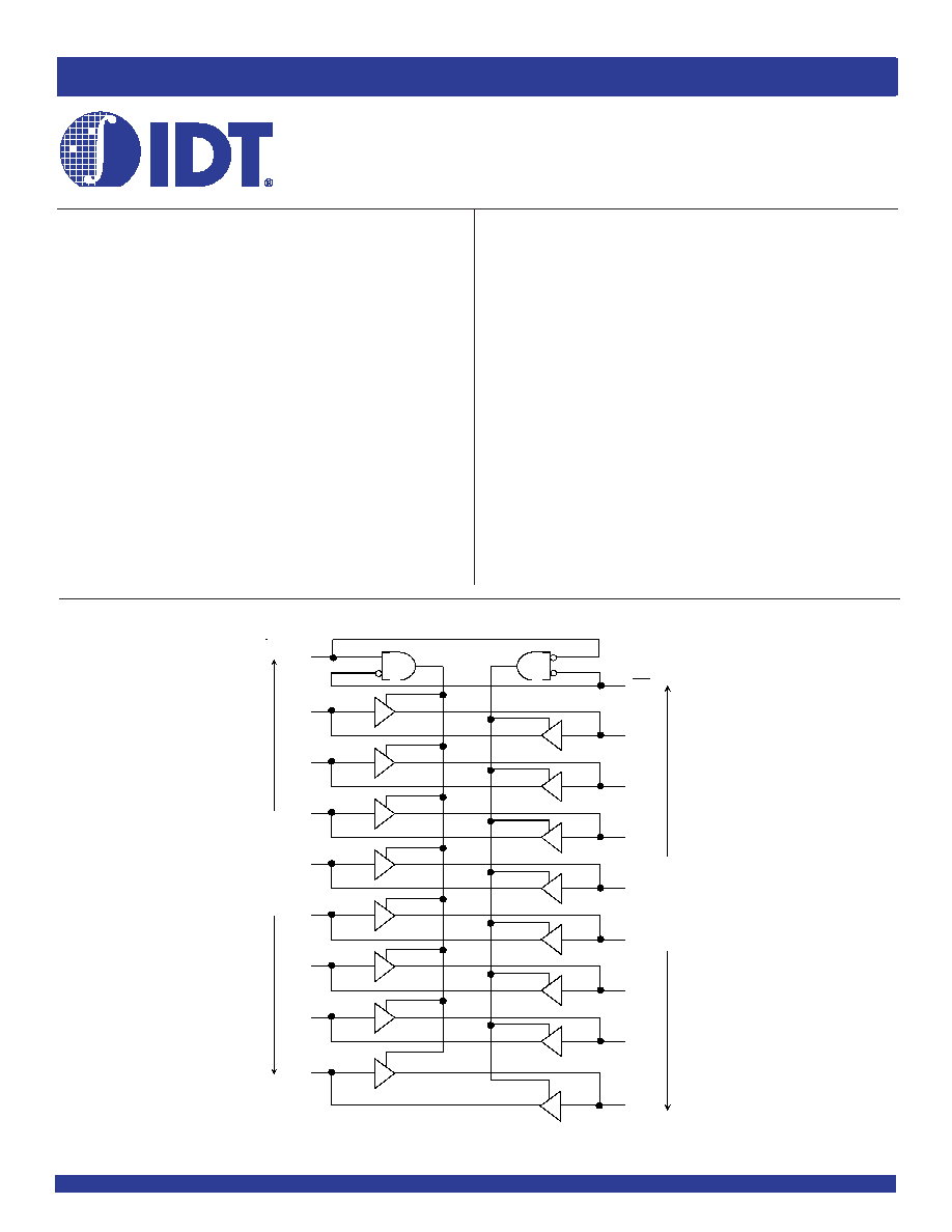
FUNCTIONAL BLOCK DIAGRAM
APPLICATIONS:
Ę 5V and 3.3V mixed voltage systems
Ę Data communication and telecommunication systems
DRIVE FEATURES:
Ę High Output Drivers: ▒24mA
Ę Reduced system switching noise
IDT74LVCC3245A
DESCRIPTION:
The LVCC3245A is manufactured using advanced dual metal CMOS
technology. This 8-bit (octal) noninverting bus transceiver contains two
separate supply rails. The B port is designed to track V
CCB
, which accepts
voltages from 3V to 5.5V, and the A port is designed to track V
CCA
, which
operates at 2.3V to 3.6V. This allows for translation from a 3.3V to a 5V
system environment and vice-versa, or from a 2.5V to a 3.3V system
environment, and vice-versa.
This LVCC3245A is ideal for asynchronous communication between two
data buses (A and B). The device transmits data from A to B or from B to
A, depending on the logic level at the direction-control (DIR) input. The
output-enable (OE) input can be used to disable the device so the buses are
effectively isolated.
The LVCC3245A has been designed with a ▒24mA output driver. This
driver is capable of driving a moderate to heavy load while maintaining
speed performance.
CMOS OCTAL BUS
TRANSCEIVER WITH ADJUSTABLE
OUTPUT VOLTAGE, 3-STATE OUT-
PUTS, 5 VOLT TOLERANT I/O
DIR
A
1
A
2
A
3
A
4
A
5
A
6
A
7
A
8
B
8
B
7
B
6
B
5
B
4
B
3
B
2
B
1
OE
2
3
4
5
6
7
8
9
10
14
15
16
17
18
19
20
21
22
2
.
3
V
t
o
3
.
6
V
P
o
r
t
3
V
t
o
5
.
5
V
P
o
r
t
INDUSTRIAL TEMPERATURE RANGE
2
IDT74LVCC3245A
CMOS OCTAL BUS TRANSCEIVER WITH ADJUSTABLE OUTPUT
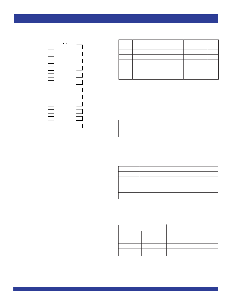
PIN CONFIGURATION
SOIC/ SSOP/ QSOP/ TSSOP
TOP VIEW
Pin Names
Description
OE
Output Enable Input (Active LOW)
DIR
Direction Control Input
A x
Port A Inputs or 3-State Outputs
B x
Port B Inputs or 3-State Outputs
N C
No Internal Connection
PIN DESCRIPTION
NOTE:
1. H = HIGH Voltage Level
L = LOW Voltage Level
X = Don't Care
Inputs
OE
DIR
Outputs
L
L
Bus B Data to Bus A
L
H
Bus A Data to Bus B
H
X
High Z state
FUNCTION TABLE
(1)
NOTE:
1. As applicable to the device type.
Symbol Parameter
(1)
Conditions
Typ.
Unit
C
IN
Input Capacitance
V
IN
= 0V
4.5
pF
C
I/O
I/O Port Capacitance
V
IN
= 0V
11
pF
CAPACITANCE
(T
A
= +25░C, F = 1.0MHz)
ABSOLUTE MAXIMUM RATINGS
FOR V
CCB
OR V
CCB
(1)
Symbol
Description
Max
Unit
V
TERM
Terminal Voltage with Respect to GND
Ł0.5 to +6
V
T
STG
Storage Temperature
Ł65 to +150
░C
I
OUT
DC Output Current
Ł50 to +50
mA
I
IK
Continuous Clamp Current,
Ł50
mA
I
OK
V
I
< 0 or V
O
< 0
I
CC
Continuous Current through each
▒100
mA
I
SS
V
CC
or GND
NOTE:
1. Stresses greater than those listed under ABSOLUTE MAXIMUM RATINGS may cause
permanent damage to the device. This is a stress rating only and functional operation
of the device at these or any other conditions above those indicated in the operational
sections of this specification is not implied. Exposure to absolute maximum rating
conditions for extended periods may affect reliability.
2
3
1
A
1
20
19
18
B
4
B
3
B
5
B
1
B
2
15
B
7
B
8
16
9
GND
10
A
8
B
6
23
22
24
21
17
DIR
5
6
A
6
7
A
4
A
5
4
A
2
A
3
8
A
7
OE
13
14
11
GND
12
V
CCB
(3V to 5.5V)
NC
GND
(2.3V to 3.6V) V
CCA
INDUSTRIAL TEMPERATURE RANGE
IDT74LVCC3245A
CMOS OCTAL BUS TRANSCEIVER WITH ADJUSTABLE OUTPUT
3
Symbol
Parameter
Test Conditions
Min.
Typ.
(2)
Max.
Unit
V
IH
Input HIGH Voltage Level
V
OB
0.1V
V
CCA
= 2.3V, V
CCB
= 3V
1.7
--
--
V
V
OB
V
CCB
- 0.1V
V
CCA
= 2.7V to 3.6V
2
--
--
V
IL
Input LOW Voltage Level
V
CCA
= 2.3V, V
CCB
= 3V
--
--
0.7
V
V
CCA
= 2.7V to 3.6V
--
--
0.8
I
IH
Input Leakage Current
V
CCA
= 3.6V
V
I
= 0 to 5.5V
--
--
▒1
ĄA
I
IL
I
OZH
High Impedance Output Current
V
CCA
= 3.6V
V
O
= V
CCA
or GND
--
--
▒5
ĄA
I
OZL
(3-State Output pins)
I
OFF
Input/Output Power Off Leakage
V
CCA
= 0V, V
IN
or V
O
5.5V
--
--
▒50
ĄA
V
H
Input Hysteresis
V
CCA
= 3.3V
--
100
--
mV
I
CCL
Quiescent Power Supply Current
V
CCA
= 3.6V
V
IN
= GND or V
CC
--
--
50
ĄA
I
CCH
I
CCZ
I
CC
Quiescent Power Supply Current
One input at V
CCA
- 0.6, other inputs at V
CCA
or GND
--
--
500
ĄA
Variation
DC ELECTRICAL CHARACTERISTICS OVER OPERATING RANGE (A PORT)
Following Conditions Apply Unless Otherwise Specified:
Operating Condition: T
A
= Ł40░C to +85░C, V
CCA
= 2.3V to 3.6V
(1)
NOTES:
1. V
CCB
= 3V to 5.5V.
2. Typical values are at V
CC
= 3.3V, +25░C ambient.
3. This applies in the disabled state only.
Symbol
Parameter
Test Conditions
Min.
Typ.
(2)
Max.
Unit
V
IH
Input HIGH Voltage Level
V
OA
0.1V
V
CCB
= 3V to 3.6V
2
--
--
V
V
OA
V
CCA
- 0.1V
V
CCB
= 5.5V
3.85
--
--
V
IL
Input LOW Voltage Level
V
CCB
= 3V to 3.6V
--
--
0.8
V
V
CCB
= 5.5V
--
--
1.65
I
IH
Input Leakage Current
V
CCB
= 3.6V
V
I
= 0 to 5.5V
--
--
▒1
ĄA
I
IL
I
OZH
High Impedance Output Current
V
CCB
= 3.6V
V
O
= V
CCB
or GND
--
--
▒5
ĄA
I
OZL
(3-State Output pins)
I
OFF
Input/Output Power Off Leakage
V
CCB
= 0V, V
IN
or V
O
5.5V
--
--
▒50
ĄA
V
H
Input Hysteresis
V
CCB
= 3.3V
--
100
--
mV
I
CCL
Quiescent Power Supply Current
V
CCB
= 3.6V
V
IN
= GND or V
CC
--
--
50
ĄA
I
CCH
V
CCB
= 5.5V
--
--
80
I
CCZ
I
CC
Quiescent Power Supply Current
One input at V
CCB
- 2.1 other inputs at V
CCB
or GND
--
--
1.5
mA
Variation
DC ELECTRICAL CHARACTERISTICS OVER OPERATING RANGE (B PORT)
Following Conditions Apply Unless Otherwise Specified:
Operating Condition: T
A
= Ł40░C to +85░C, V
CCB
= 3V to 5.5V
(1)
NOTES:
1. V
CCA
= 2.3V to 3.6V.
2. Typical values are at V
CC
= 3.3V, +25░C ambient.
3. This applies in the disabled state only.
INDUSTRIAL TEMPERATURE RANGE
4
IDT74LVCC3245A
CMOS OCTAL BUS TRANSCEIVER WITH ADJUSTABLE OUTPUT
NOTE:
1. V
IH
and V
IL
must be within the min. or max. range shown in the DC ELECTRICAL CHARACTERISTICS OVER OPERATING RANGE table for the appropriate V
CC
range.
T
A
= Ł 40░C to + 85░C, V
CCB
= 3V to 5.5V.
OUTPUT DRIVE CHARACTERISTICS, V
CCA
= 2.3V TO 3.6V (A PORT)
NOTE:
1. V
IH
and V
IL
must be within the min. or max. range shown in the DC ELECTRICAL CHARACTERISTICS OVER OPERATING RANGE table for the appropriate V
CC
range.
T
A
= Ł 40░C to + 85░C, V
CCA
= 2.3V to 3.6V.
OUTPUT DRIVE CHARACTERISTICS, V
CCB
= 3V TO 5.5V (B PORT)
OPERATING CHARACTERISTICS, T
A
= 25░C
V
CCA
= 3.3V, V
CCB
= 5V
Symbol
Parameter
Test Conditions
Typical
Unit
C
PD
Power Dissipation Capacitance per Transceiver Outputs enabled A to B
C
L
= 0pF, f = 10Mhz
38
pF
C
PD
Power Dissipation Capacitance per Transceiver Outputs disabled B to A
36.5
Symbol
Parameter
Test Conditions
(1)
Min.
Max.
Unit
V
OHA
Output HIGH Voltage
V
CCA
= 3V
V
CCB
= 3V
I
OH
= Ł 0.1mA
2.9
--
V
(B port to A port)
V
CCA
= 2.3V
V
CCB
= 3V
I
OH
= Ł 8mA
2
--
V
CCA
= 2.7V
V
CCB
= 3V
I
OH
= Ł 12mA
2.2
--
V
CCA
= 3V
V
CCB
= 3V
2.4
--
V
CCA
= 3V
V
CCB
= 3V
I
OH
= Ł 24mA
2.2
--
V
CCA
= 2.7V
V
CCB
= 4.5V
2
--
V
OLA
Output LOW Voltage
V
CCA
= 3V
V
CCB
= 3V
I
OL
= 0.1mA
--
0.1
V
(B port to A port)
V
CCA
= 2.3V
V
CCB
= 3V
I
OL
= 8mA
--
0.6
V
CCA
= 2.7V
V
CCB
= 3V
I
OL
= 12mA
--
0.5
V
CCA
= 3V
V
CCB
= 3V
I
OL
= 24mA
--
0.5
V
CCA
= 2.7V
V
CCB
= 4.5V
--
0.5
Symbol
Parameter
Test Conditions
(1)
Min.
Max.
Unit
V
OHB
Output HIGH Voltage
V
CCB
= 3V
V
CCA
= 3V
I
OH
= Ł 0.1mA
2.9
--
V
(A port to B port)
V
CCB
= 3V
V
CCA
= 2.3V
I
OH
= Ł 12mA
2.4
--
V
CCB
= 3V
V
CCA
= 2.7V
2.4
--
V
CCB
= 3V
V
CCA
= 3V
I
OH
= Ł 24mA
2.2
--
V
CCB
= 4.5V
V
CCA
= 2.7V
3.2
--
V
OLB
Output LOW Voltage
V
CCB
= 3V
V
CCA
= 3V
I
OL
= 0.1mA
--
0.1
V
(A port to B port)
V
CCB
= 3V
V
CCA
= 2.3V
I
OL
= 12mA
--
0.4
V
CCB
= 3V
V
CCA
= 3V
I
OL
= 24mA
--
0.5
V
CCB
= 4.5V
V
CCA
= 3V
--
0.5
INDUSTRIAL TEMPERATURE RANGE
IDT74LVCC3245A
CMOS OCTAL BUS TRANSCEIVER WITH ADJUSTABLE OUTPUT
5
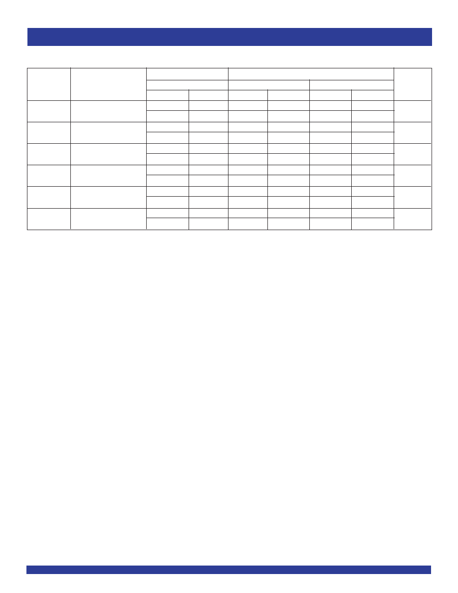
SWITCHING CHARACTERISTICS
(1)
V
CCA
= 2.5V ▒ 0.2V
V
CCA
= 2.7V to 3.6V
V
CCB
= 3.3V ▒ 0.3V
V
CCB
= 5V ▒ 0.5V
V
CCB
= 3.3V ▒ 0.3V
Symbol
Parameter
Min.
Max.
Min.
Max.
Min.
Max.
Unit
t
PHL
Propagation Delay
1
9.4
1
6
1
7.1
ns
t
PLH
Ax to Bx
1
9.1
1
5.3
1
7.2
t
PHL
Propagation Delay
1
11.2
1
5.8
1
6.4
ns
t
PLH
Bx to Ax
1
9.9
1
7
1
7.6
t
PZL
Output Enable Time
1
13
1
8.1
1
9.2
ns
t
PLZ
OE to Bx
1
12.8
1
8.4
1
9.9
t
PZL
Output Enable Time
1
14.5
1
9.2
1
9.7
ns
t
PLZ
OE to Ax
1
12.9
1
9.5
1
9.5
t
PLZ
Output Disable Time
1
7.1
1
5.5
1
6.6
ns
t
PHZ
OE to Ax
1
6.9
1
7.8
1
6.9
t
PLZ
Output Disable Time
1
8.8
1
7.3
1
7.5
ns
t
PHZ
OE to Bx
1
8.9
1
7
1
7.9
NOTE:
1. See TEST CIRCUITS AND WAVEFORMS. T
A
= Ł 40░C to + 85░C.