
INDUSTRIAL TEMPERATURE RANGE
IDT74ALVCH16652
3.3V CMOS 16-BIT BUS TRANSCEIVER AND REGISTER
1
OCTOBER 1999
INDUSTRIAL TEMPERATURE RANGE
The IDT logo is a registered trademark of Integrated Device Technology, Inc.
© 1999 Integrated Device Technology, Inc.
DSC-4526/1
FEATURES:
· 0.5 MICRON CMOS Technology
· Typical t
SK(o)
(Output Skew) < 250ps
· ESD > 2000V per MIL-STD-883, Method 3015; > 200V using
machine model (C = 200pF, R = 0)
· V
CC
= 3.3V ± 0.3V, Normal Range
· V
CC
= 2.7V to 3.6V, Extended Range
· V
CC
= 2.5V ± 0.2V
· CMOS power levels (0.4
µµ
µµ
µ W typ. static)
· Rail-to-Rail output swing for increased noise margin
· Available in SSOP, TSSOP, and TVSOP packages
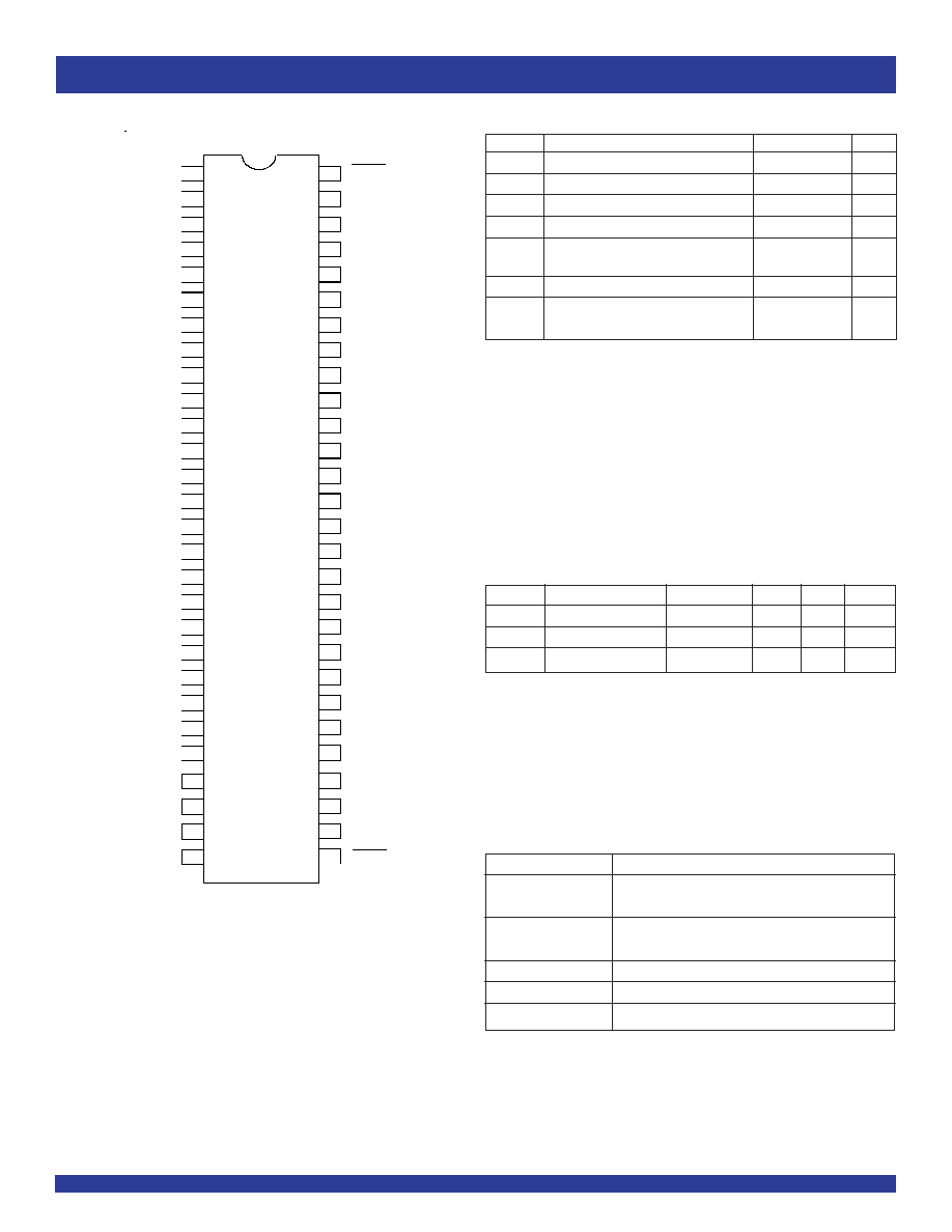
FUNCTIONAL BLOCK DIAGRAM
DESCRIPTION:
This 16-bit bus transceiver and register is built using advanced dual metal
CMOS technology. The ALVCH16652 consists of D-type flip-flops and control
circuitry arranged for multiplexed transmission of data directly from the data bus
or from the internal storage registers. The device can be used as two 8-bit
transceivers or one 16-bit transceiver.
Complementary output enable (OEAB and OEBA) inputs are provided to
control the transceiver functions. Select control (SAB and SBA) inputs are
provided to select whether real-time or stored data is transferred. A low input
level selects real-time data, and a high input level selects stored data. Circuitry
used for select control eliminates the typical decoding glitch that occurs in a
multiplexer during the transition between stored and real-time data. Data on the
A or B bus, or both, can be stored in the internal D flip-flops by low-to-high
transition at the appropriate clock (CLKAB or CLKBA) inputs regardless of the
levels on the select control or output enable inputs. When SAB and SBA are in
the real-time transfer mode, it also is possible to store data without using the
internal D-type flip-flops by simultaneously enabling OEAB and OEBA. In this
configuration, each output reinforces its input. Thus, when all other data sources
to the two sets of bus lines are in the high-impedance state, each set of bus lines
remains at its last level configuration.
The ALVCH16652 has been designed with a ±24mA output driver. This
driver is capable of driving a moderate to heavy load while maintaining speed
performance.
The ALVCH16652 has "bus-hold" which retains the inputs' last state
whenever the input bus goes to a high impedance. This prevents floating inputs
and eliminates the need for pull-up/down resistors.
DRIVE FEATURES:
· High Output Drivers: ±24mA
· Suitable for heavy loads
APPLICATIONS:
· 3.3V high speed systems
· 3.3V and lower voltage computing systems
IDT74ALVCH16652
3.3V CMOS 16-BIT BUS
TRANSCEIVER AND
REGISTER WITH 3-STATE
OUTPUTS AND BUS-HOLD
TO 7 OTHER CHANNELS
1
B
1
D
C
D
C
1
A
1
1
SAB
1
CLKAB
1
SBA
1
OEBA
1
CLKBA
56
55
54
2
3
5
52
1
OEAB
1
A REG
B REG
TO 7 OTHER CHANNELS
2
B
1
D
C
D
C
2
A
1
2
SAB
2
CLKAB
2
SBA
2
OEBA
2
CLKBA
29
30
31
27
26
15
42
2
OEAB
28
A REG
B REG
INDUSTRIAL TEMPERATURE RANGE
2
IDT74ALVCH16652
3.3V CMOS 16-BIT BUS TRANSCEIVER AND REGISTER
SSOP/ TSSOP/ TVSOP
TOP VIEW
PIN CONFIGURATION
Symbol
Description
Max
Unit
V
TERM
(2)
Terminal Voltage with Respect to GND
0.5 to +4.6
V
V
TERM
(3)
Terminal Voltage with Respect to GND
0.5 to V
CC
+0.5
V
T
STG
Storage Temperature
65 to +150
°C
I
OUT
DC Output Current
50 to +50
mA
I
IK
Continuous Clamp Current,
±50
mA
V
I
< 0 or V
I
> V
CC
I
OK
Continuous Clamp Current, V
O
< 0
50
mA
I
CC
Continuous Current through each
±100
mA
I
SS
V
CC
or GND
ABSOLUTE MAXIMUM RATINGS
(1)
NOTES:
1. Stresses greater than those listed under ABSOLUTE MAXIMUM RATINGS may cause
permanent damage to the device. This is a stress rating only and functional operation
of the device at these or any other conditions above those indicated in the operational
sections of this specification is not implied. Exposure to absolute maximum rating
conditions for extended periods may affect reliability.
2. V
CC
terminals.
3. All terminals except V
CC
.
NOTE:
1. As applicable to the device type.
Symbol
Parameter
(1)
Conditions
Typ.
Max.
Unit
C
IN
Input Capacitance
V
IN
= 0V
5
7
pF
C
OUT
Output Capacitance
V
OUT
= 0V
7
9
pF
C
I/O
I/O Port Capacitance
V
IN
= 0V
7
9
pF
CAPACITANCE
(T
A
= +25°C, F = 1.0MHz)
NOTE:
1. These pins have "Bus-Hold". All other pins are standard inputs, outputs, or I/Os.
Pin Names
Description
xAx
Data Register A Inputs
(1)
Data Register B Outputs
xBx
Data Register B Inputs
(1)
Data Register A Outputs
xCLKAB, xCLKBA
Clock Pulse Inputs
xSAB, xSBA
Output Data Source Select Inputs
xOEAB, xOEBA
Output Enable Inputs
PIN DESCRIPTION
1
OEAB
1
SAB
GND
1
A
1
V
CC
GND
GND
V
CC
GND
1
CLKAB
1
A
2
1
A
3
1
A
4
1
A
5
1
A
6
1
A
7
1
A
8
2
A
1
2
A
2
2
A
3
2
A
4
2
A
5
2
A
6
2
A
7
2
A
8
2
SAB
2
CLKAB
2
OEAB
1
OEBA
1
SBA
GND
1
B
1
V
CC
GND
GND
V
CC
GND
1
CLKBA
1
B
2
1
B
3
1
B
4
1
B
5
1
B
6
1
B
8
2
B
1
2
B
2
2
B
3
2
B
4
2
B
5
2
B
6
2
B
7
2
B
8
2
SBA
2
CLKBA
2
OEBA
1
B
7
2
3
4
5
6
7
8
9
10
11
12
13
14
15
16
17
18
19
20
21
22
23
24
47
46
45
44
43
42
41
40
39
38
37
36
35
34
33
48
49
50
51
52
53
54
55
56
1
25
26
27
28
32
31
30
29

INDUSTRIAL TEMPERATURE RANGE
IDT74ALVCH16652
3.3V CMOS 16-BIT BUS TRANSCEIVER AND REGISTER
3
Symbol
Parameter
Test Conditions
Min.
Typ.
(1)
Max.
Unit
V
IH
Input HIGH Voltage Level
V
CC
= 2.3V to 2.7V
1.7
--
--
V
V
CC
= 2.7V to 3.6V
2
--
--
V
IL
Input LOW Voltage Level
V
CC
= 2.3V to 2.7V
--
--
0.7
V
V
CC
= 2.7V to 3.6V
--
--
0.8
I
IH
Input HIGH Current
V
CC
= 3.6V
V
I
= V
CC
--
--
±5
µA
I
IL
Input LOW Current
V
CC
= 3.6V
V
I
= GND
--
--
±5
µA
I
OZH
High Impedance Output Current
V
CC
= 3.6V
V
O
= V
CC
--
--
±10
µA
I
OZL
(3-State Output pins)
V
O
= GND
--
--
±10
V
IK
Clamp Diode Voltage
V
CC
= 2.3V, I
IN
= 18mA
--
0.7
1.2
V
V
H
Input Hysteresis
V
CC
= 3.3V
--
100
--
mV
I
CCL
Quiescent Power Supply Current
V
CC
= 3.6V
--
0.1
40
µA
I
CCH
V
IN
= GND or V
CC
I
CCZ
I
CC
Quiescent Power Supply Current
One input at V
CC
- 0.6V, other inputs at V
CC
or GND
--
--
750
µA
Variation
DC ELECTRICAL CHARACTERISTICS OVER OPERATING RANGE
Following Conditions Apply Unless Otherwise Specified:
Operating Condition: T
A
= 40°C to +85°C
NOTE:
1. Typical values are at V
CC
= 3.3V, +25°C ambient.
FUNCTION TABLE
(1)
Inputs
Data I/O
(2)
xOEAB
xOEBA
xCLKAB
xCLKBA
xSAB
xSBA
xAx
xBx
Operation or Function
L
H
H or L
H or L
X
X
Input
Input
Isolation
L
H
X
X
Input
Input
Store A and B Data
X
H
H or L
X
X
Input
Unspecified
(3)
Store A, hold B
H
H
X
(3)
X
Input
Output
Store A in both registers
L
X
H or L
X
X
Unspecified
(3)
Input
Hold A, store B
L
L
X
X
(3)
Output
Input
Store B in both registers
L
L
X
X
X
L
Output
Input
Real time B data to A bus
L
L
X
H or L
X
H
Output
Input
Stored B data to A bus
H
H
X
X
L
X
Input
Output
Real time A data to B bus
H
H
H or L
X
H
X
Input
Output
Stored A data to B bus
H
L
H or L
H or L
H
H
Input
Output
Stored A data to B Bus and
Stored B data to A bus
NOTES:
1. H = HIGH Voltage Level
L = LOW Voltage Level
X = Don't Care
= LOW-to-HIGH Transition
2. The data output functions may be enabled or disabled by various signals at the xOEAB or xOEBA inputs. Data input functions are always enabled, i.e. data at the bus pins will
be stored on every LOW-to-HIGH transition on the clock inputs.
3. Select control = L: clocks can occur simultaneously.
Select control = H: clocks must be staggered to load both registers.

INDUSTRIAL TEMPERATURE RANGE
4
IDT74ALVCH16652
3.3V CMOS 16-BIT BUS TRANSCEIVER AND REGISTER
BUS
A
BUS
B
xOEAB
L
xOEBA
L
xCLKAB
X
xCLKBA
X
xSAB
X
xSBA
L
BUS
A
BUS
B
xCLKAB
X
xCLKBA
X
xSAB
L
xSBA
X
BUS
A
BUS
B
xOEAB
X
L
L
xOEBA
H
X
H
xCLKAB
X
xCLKBA
X
xSAB
X
X
X
xSBA
X
X
X
BUS
A
BUS
B
xOEAB
H
xOEBA
L
xCLKAB
H or L
xCLKBA
H or L
xSAB
H
xSBA
X
xOEAB
H
xOEBA
H
Storage from A and/or B
Transfer Stored Data to A and/or B
Real-Time Transfer Bus B to Bus A
Real-Time Transfer Bus A to Bus B
BUS MANAGEMENT FUNCTIONS
INDUSTRIAL TEMPERATURE RANGE
IDT74ALVCH16652
3.3V CMOS 16-BIT BUS TRANSCEIVER AND REGISTER
5
NOTE:
1. V
IH
and V
IL
must be within the min. or max. range shown in the DC ELECTRICAL CHARACTERISTICS OVER OPERATING RANGE table for the appropriate V
CC
range.
T
A
= 40°C to + 85°C.
OUTPUT DRIVE CHARACTERISTICS
Symbol
Parameter
Test Conditions
(1)
Min.
Max.
Unit
V
OH
Output HIGH Voltage
V
CC
= 2.3V to 3.6V
I
OH
= 0.1mA
V
CC
0.2
--
V
V
CC
= 2.3V
I
OH
= 6mA
2
--
V
CC
= 2.3V
I
OH
= 12mA
1.7
--
V
CC
= 2.7V
2.2
--
V
CC
= 3V
2.4
--
V
CC
= 3V
I
OH
= 24mA
2
--
V
OL
Output LOW Voltage
V
CC
= 2.3V to 3.6V
I
OL
= 0.1mA
--
0.2
V
V
CC
= 2.3V
I
OL
= 6mA
--
0.4
I
OL
= 12mA
--
0.7
V
CC
= 2.7V
I
OL
= 12mA
--
0.4
V
CC
= 3V
I
OL
= 24mA
--
0.55
OPERATING CHARACTERISTICS, T
A
= 25°C
V
CC
= 2.5V ± 0.2V
V
CC
= 3.3V ± 0.3V
Symbol
Parameter
Test Conditions
Typical
Typical
Unit
C
PD
Power Dissipation Capacitance Outputs enabled
C
L
= 0pF, f = 10Mhz
pF
C
PD
Power Dissipation Capacitance Outputs disabled
BUS-HOLD CHARACTERISTICS
Symbol
Parameter
(1)
Test Conditions
Min.
Typ.
(2)
Max.
Unit
I
BHH
Bus-Hold Input Sustain Current
V
CC
= 3V
V
I
= 2V
75
--
--
µA
I
BHL
V
I
= 0.8V
75
--
--
I
BHH
Bus-Hold Input Sustain Current
V
CC
= 2.3V
V
I
= 1.7V
45
--
--
µA
I
BHL
V
I
= 0.7V
45
--
--
I
BHHO
Bus-Hold Input Overdrive Current
V
CC
= 3.6V
V
I
= 0 to 3.6V
--
--
±500
µA
I
BHLO
NOTES:
1. Pins with Bus-Hold are identified in the pin description.
2. Typical values are at V
CC
= 3.3V, +25°C ambient.