
MK1573-02
GenClock
TM
HSYNC to Video Clock
MDS 1573-02 B
1
Revision 120497
Printed 11/15/00
Integrated Circuit Systems, Inc. · 525 Race Street · San Jose · CA · 95126·(408)295-9800tel·www.icst.com
· Packaged in 16 pin narrow (150 mil) SOIC
· The -02 version has one frequency changed
(32MHz was added), and tracks the HSYNC
better than the -01 version.
· Exact ratios stored in the device eliminate the need
for external dividers
· Accepts HSYNC of 15.625kHz or 15.73426kHz
· Highly accurate frequency generation within 1 ppm
· Generates NTSC/PAL subcarrier frequencies, and
4X and 8X of those frequencies
· Generates 27MHz and 13.5MHz
· 2X HSYNC clock available
· Recovered HSYNC clock available
· Inverted HSYNC clock available
· 4.5V to 5.5V operation
The MK1573 GenClockTM provides genlock
timing for video overlay systems. The device
accepts the horizontal sync (HSYNC) signal as the
input reference clock, and generates a frequency-
locked high speed output. Stored in the device are
the multipliers for 16 combinations of popular
frequencies for analog and digital TV and set-top
box systems. Frequency-locked outputs include
1X, 4X, and 8X the subcarrier frequencies of
NTSC and PAL systems, and 27MHz plus
13.5MHz for digital video systems. In most
selections, the chip recovers the HSYNC clock by
outputting a low jitter 50% duty cycle version of
HSYNC. Also available is an inverted recovered
HSYNC clock, and a double speed recovered
HSYNC clock.
MicroClock can customize this device for any
other different frequencies.
Block Diagram
Description
Features
Input
Buffer
VDD
GND
Clock
Synthesis
and
Control
Circuitry
HSYNC
Input Clock
Output
Buffer
Output
Buffer
CLK1
2
2
Output
Buffer
CLK2
FS0-3
CLK3
4
OE (all outputs)

MK1573-02
GenClock
TM
HSYNC to Video Clock
MDS 1573-02 B
2
Revision 120497
Printed 11/15/00
Integrated Circuit Systems, Inc. · 525 Race Street · San Jose · CA · 95126·(408)295-9800tel·www.icst.com
Number
Name
Type Description
1
HSYNC
I
HSYNC clock input. The output clocks are synchronized to the HSYNC falling edge.
2
VDD
P
Connect to +5V.
3
VDD
P
Connect to +5V.
4
CAP1
I
Connect a 0.01µF ceramic capacitor and a 39k
resistor in series between this pin and CAP2.
5
GND
P
Connect to ground.
6
CAP2
I
Connect a 0.01µF ceramic capacitor and a 39k
resistor in series between this pin and CAP1.
7
GND
P
Connect to ground.
8
FS0
I
Frequency Select 0. Determines CLK outputs (with given input) per table above.
9
CLK3
O
Clock 3 determined by status of FS3:0 per table above.
10
CLK1
O
Clock 1 determined by status of FS3:0 per table above.
11
OE
I
Output Enable. Tri-states the three output clocks when low.
12
CLK2
O
Clock 2 determined by status of FS3:0 per table above.
13
FS1
I
Frequency Select 1. Determines CLK outputs (with given input) per table above.
14
FS2
I
Frequency Select 2. Determines CLK outputs (with given input) per table above.
15
N/C
-
No Connect. Nothing is connected to this pin.
16
FS3
I
Frequency Select 3. Determines CLK outputs (with given input) per table above.
Pin Descriptions
Type: I = Input, O = output, P = power supply connection
Pin Assignment
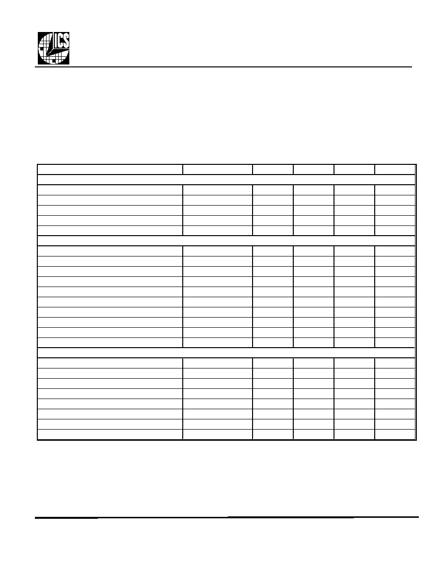
Output Clocks Decoding Table MK1573-02 (MHz)
16 pin (150 mil) SOIC
1
16
2
3
4
15
14
13
CAP1
GND
VDD
FS1
OE
5
6
7
8
12
11
10
9
FS0
FS2
CAP2
FS3
CLK2
CLK3
GND
CLK1
VDD
HSYNC
N/C
· 0 = connect directly to ground, 1 = connect directly to VDD.
· CLK2 is a recovered HSYNC (with 50% duty cycle) on selections in italic.
· HSYNC reference outputs on CLK3 (in italic) are inverted, recovered HSYNC.
Decode Address HSYNC
Multiplier
CLK 1
CLK 2
CLK 3
FS3:0
(Hex)
pin 1
On-chip
pin 10
pin 12
pin 9
0
15.625k
1536
24M
12M
15.625k
1
15.734264k 1525 1/3
24M
12M
15.734264k
2
15.625k
1728
27M
13.5M
15.625k
3
15.734264k
1716
27M
13.5M
15.734264k
4
15.625k
960
15M
7.5M
15.625k
5
15.734264k
953 1/3
15M
7.5M
15.734264k
6
15.625k
3840
60M
30M
15.625k
7
15.734264k
3840
60.41957M 30.20979M 15.734264k
8
15.625k
2270
35.46875M 17.734375M 4.433594M
9
15.734264k
1820
28.63636M 14.31818M 3.579545M
A
15.625k
2270
35.46875M
15.625k
15.625k
B
15.734264k
1820
28.63636M 15.734264k 15.734264k
C
15.625k
2048
32M
16M
15.625k
D
15.734264k
808
12.71329M 15.734264k
31.4685k
E
15.625k
2270
35.46875M
15.625k
31.25k
F
15.734264k
1820
28.63636M 15.734264k
31.4685k
0000
0001
0010
0011
0100
0101
0110
0111
1000
1001
1010
1011
1100
1101
1110
1111
MK1573-02
GenClock
TM
HSYNC to Video Clock
MDS 1573-02 B
3
Revision 120497
Printed 11/15/00
Integrated Circuit Systems, Inc. · 525 Race Street · San Jose · CA · 95126·(408)295-9800tel·www.icst.com
Parameter
Conditions
Minimum
Typical
Maximum
Units
ABSOLUTE MAXIMUM RATINGS (Note 1)
ABSOLUTE MAXIMUM RATINGS (Note 1)
Supply Voltage, VDD
Referenced to GND
7
V
Inputs and Clock Outputs
-0.5
VDD+0.5
V
Ambient Operating Temperature
0
70
°C
Soldering Temperature
Max of 10 seconds
250
°C
Storage Temperature
-65
150
°C
DC CHARACTERISTICS (VDD = 5V unless noted)
DC CHARACTERISTICS (VDD = 5V unless noted)
Operating Voltage, VDD
4.5
5.5
V
Input High Voltage, VIH
2
V
Input Low Voltage, VIL
0.8
V
Output High Voltage
IOH=-4mA
VDD-0.4
V
Output High Voltage
IOH=-25mA
2.4
V
Output Low Voltage
IOL=25mA
0.4
V
Operating Supply Current, IDD
No Load, VDD=5.0V
15
mA
Short Circuit Current
Each output
±100
mA
Input Capacitance
7
pF
Actual mean frequency error versus target, note 2
Any clock selection
0
1
ppm
AC CHARACTERISTICS (VDD = 5V unless noted)
AC CHARACTERISTICS (VDD = 5V unless noted)
Input Frequency, NTSC
15.734264
kHz
Input Frequency, PAL
15.625
kHz
Output Clock Rise Time
0.8 to 2.0V
1.5
ns
Output Clock Fall Time
2.0 to 0.8V
1.5
ns
Output Clock Duty Cycle, High Time
At VDD/2
40
49 to 51
60
%
Absolute Clock Period Jitter
TBD
ps
Output Enable Time, OE high to outputs on
50
ns
Output Disable Time, OE low to tri-state
3
µs
Notes:
1. Stresses beyond those listed under Absolute Maximum Ratings could cause permanent damage to the device. Prolonged exposure
to levels above the operating limits but below the Absolute Maximums may affect device reliability.
2. Most selections have zero ppm error. Some selections have a maximum of 1 ppm synthesis error .
External Components/Crystal Selection
Electrical Specifications
The MK1573 requires a minimum number of external components for proper operation. A 0.1µF low
leakage capacitor (see Capacitor Selection on following page) should be connected between CAP1 and
CAP2 as close to the chip as possible. A high quality ceramic capacitor is recommended. A decoupling
capacitor of 0.1µF must be connected between VDD and GND pins (pins 2 and 3, 5 and 7) close to the
chip, and 33
terminating resistors can be used on clock outputs with traces longer than 1 inch.
MK1573-02
GenClock
TM
HSYNC to Video Clock
MDS 1573-02 B
4
Revision 120497
Printed 11/15/00
Integrated Circuit Systems, Inc. · 525 Race Street · San Jose · CA · 95126·(408)295-9800tel·www.icst.com
The series connected capacitor and resistor between CAP1 and CAP2 (pins 4 and 6) determine the dynamic
characteristics of the phase-locked loop. The capacitor must have very low leakage, therefor a high quality
ceramic capacitor is recommended. DO NOT use any type of polarized or electrolytic capacitor. The values
of the RC network determine the bandwidth of the PLL.
The tracking of the jitter on the HSYNC input improves with increasing values of R and decreasing values of
C, until a point is reached where the loop starts becoming unstable. At that point, HSYNC tracking becomes
unreliable. Loop filter values between 470pF and 0.01µF, and 18k
and 120k
will work for most
application where the PLL must track HSYNC jitter with minimum error. A good starting point is 680pF
and 82k
. The optimum values should be determined by the spectral characteristics of the HSYNC jitter.
The following formula gives the approximate loop bandwidth for the MK1573:
where:
f
bw is the loop bandwidth in Hertz
f
clk1 is the frequency of CLK1 in Hertz
C
is the value of capacitor in Farads
For example, if CLK1 is running at 24MHz and C=1000pF, then
f
bw =
f
clk1 · C
537
f
bw =
537
24x10
6
· 1x10
-9
= 3.47kHz
Loop Bandwidth and Loop Filter Component Selection
Video Clock Multipliers/Accuracies
In the table on page 2 are the actual multipliers stored in the MK1573-02 ROM, which shows that the
accuracies are within one ppm for the output clocks.
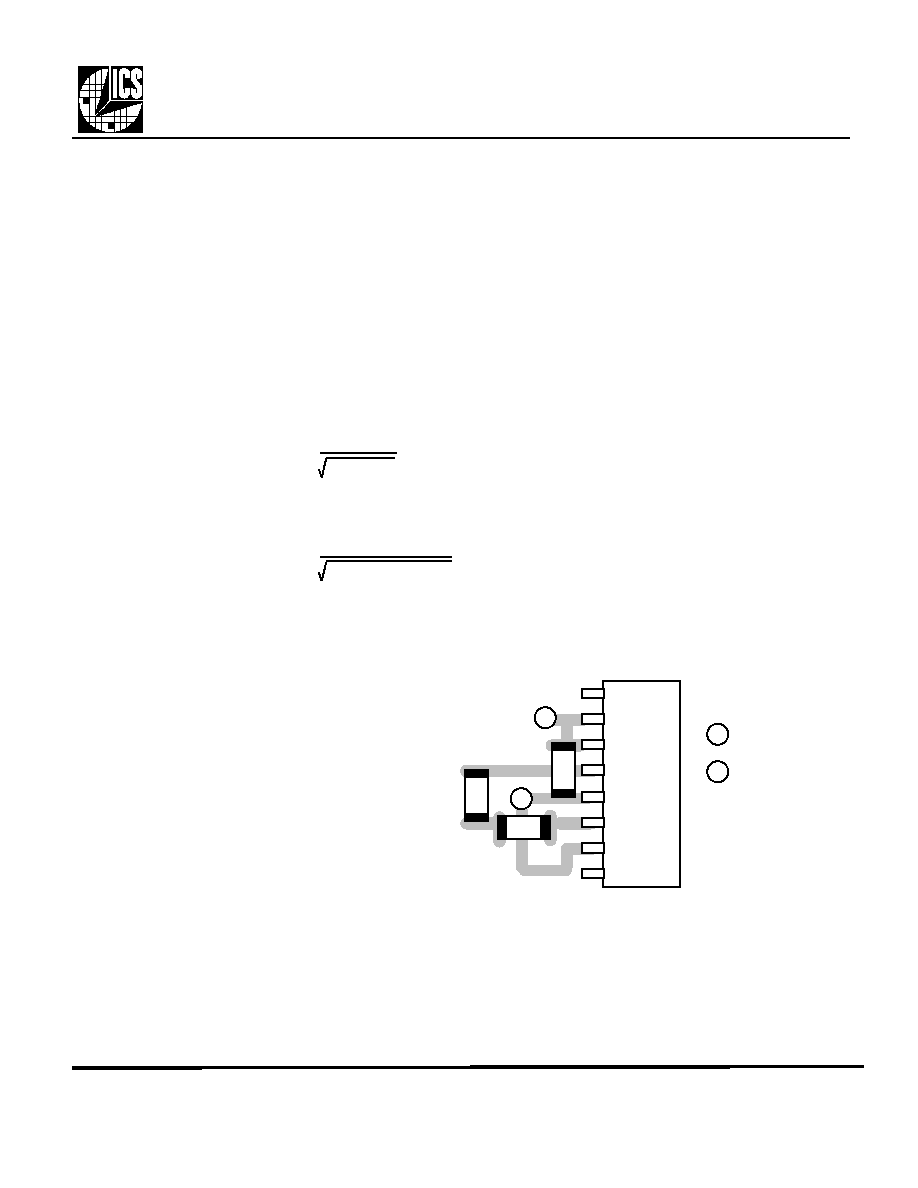
PC Board Layout
A proper board layout is critical to the successful
use of the MK1573. In particular, the CAP1 and
CAP2 pins are very sensitive to noise and leakage
(CAP1 at pin 4 is the most sensitive). Traces
must be as short as possible and the capacitor
and resistor must be mounted next to the device
as shown to the right. The capacitor connected
between pins 3 and 5 is the power supply
decoupling capacitor.
The high frequency output clocks on CLK1 and
CLK2 may benefit from a series 33
resistor
connected close to the pin (not shown).
1
2
3
4
5
6
7
8
G
V
=connect to VDD
=connect to GND
V
G
16
15
14
13
12
11
10
9
cap
If minimum absolute jitter is required, the RC network should be replaced by a single capacitor with a value
between 0.01µF and 2µF. Larger values will cause the PLL to start more slowly. For example, if C=2µF, the
loop may take several seconds to start.
cap
resist.

MK1573-02
GenClock
TM
HSYNC to Video Clock
MDS 1573-02 B
5
Revision 120497
Printed 11/15/00
Integrated Circuit Systems, Inc. · 525 Race Street · San Jose · CA · 95126·(408)295-9800tel·www.icst.com
Clock Waveforms
In addition to generating the video clock on CLK1 (pin 10), the MK1573 also outputs the recovered
HSYNC clocks. On certain selections, a double speed recovered HSYNC clock is also available. These
recovered clocks will have lower jitter than the HSYNC input due to the filtering action of the PLL. The
jitter spectrum of the recovered clocks will be reduced at frequencies higher than the loop bandwidth. The
above section describes how to calculate the approximate loop bandwidth. The waveforms of the
recovered clocks fall into one of three different groups depending on the address selection:
HSYNC
input
CLK3
Addresses 0 to 7 and C
HSYNC
input
CLK3
Addresses D, E, and F
CLK2
The recovered clocks are triggered by the falling edge of HSYNC and are delayed by about 100ns.
HSYNC
input
CLK3
Addresses A and B
CLK2
MK1573-02
GenClock
TM
HSYNC to Video Clock
MDS 1573-02 B
6
Revision 120497
Printed 11/15/00
Integrated Circuit Systems, Inc. · 525 Race Street · San Jose · CA · 95126·(408)295-9800tel·www.icst.com
b
D
E
H
e
Q
c
A
h x 45°
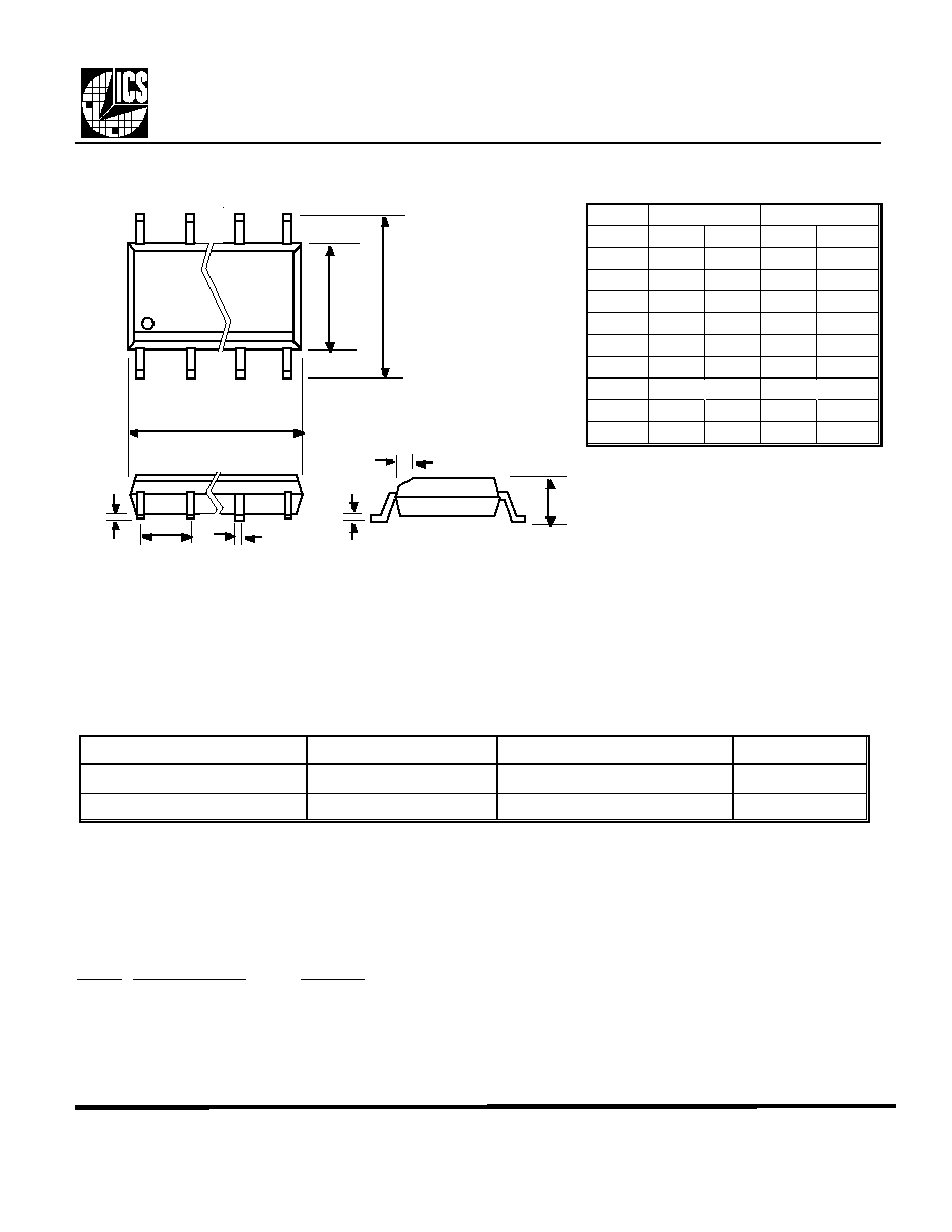
Package Outline and Package Dimensions
Ordering Information
16 pin SOIC narrow
Inches
Inches
Millimeters
Millimeters
Symbol
Min
Max
Min
Max
A
0.055
0.070
1.397
1.778
b
0.013
0.019
0.330
0.483
c
0.007
0.010
0.191
0.254
D
0.385
0.400
9.779
10.160
E
0.150
0.160
3.810
4.064
H
0.225
0.245
5.715
6.223
e .050 BSC
.050 BSC
1.27 BSC
1.27 BSC
h
0.016
0.406
Q
0.004
0.01
0.102
0.254
While the information presented herein has been checked for both accuracy and reliability, MicroClock Incorporated assumes no responsibility for either its use or for the
infringement of any patents or other rights of third parties, which would result from its use. No other circuits, patents, or licenses are implied. This product is intended for use in
normal commercial applications. Any other applications such as those requiring extended temperature range, high reliability, or other extraordinary environmental requirements
are not recommended without additional processing by MicroClock. MicroClock reserves the right to change any circuitry or specifications without notice. MicroClock does not
authorize or warrant any MicroClock product for use in life support devices or critical medical instruments.
Part/Order Number
Marking
Package
Temperature
MK1573-02S
MK1573-02S
16 pin narrow SOIC
0-70°C
MK1573-02STR
MK1573-02S
Add Tape & Reel
0-70°C
CHANGE HISTORY
Version Date first published
Comments
A
10/18/96
Original
B
12/4/97
Final version
GenClock is a trademark of MicroClock Incorporated
©1996 MicroClock Incorporated