
Integrated
Circuit
Systems, Inc.
ICS952703
Preliminary Product Preview
0813B--05/17/05
Pin Configuration
VDDREF 1
48 VDDLAPIC
**FS0/REF0 2
47 IOAPIC1
**FS1/REF1 3
46 IOAPIC0
**Mode/REF2 4
45 GNDAPIC
GNDREF 5
44 VDDSRC
X1 6
43 SRCCLKT
X2 7
42 SRCCLKC
GNDZ 8
41 GND
ZCLK0 9
40 CPUCLKODT1
ZCLK1 10
39 GNDCPU
VDDZ 11
38 CPUCLKODT0
SCLK 12
37 CPUCLKODC0
VDDPCI 13
36 AVDD
*FS2/PCICLK_F0 14
35 AGND
*FS3/PCICLK_F1 15
34 IREF
PCICLK0 16
33 SDATA
PCICLK1 17
32 GNDAGP
GNDPCI 18
31 AGPCLK0
VDDPCI 19
30 AGPCLK1
PCICLK2 20
29 VDDAGP
*(PCI_STOP#)PCICLK3 21
28 AVDD48
*(CPU_STOP#)PCICLK4 22
27 12_48MHz/SEL12_48#MHz*
*(PD#)PCICLK5 23
26 24_48MHz/SEL24_48#MHz**~
GNDPCI 24
25 GND48
48-SSOP
* Internal Pull-Up Resistor
** Internal Pull-Down Resistor
~ This output have 1.5X Drive Strength
I
C
S
952703
Recommended Application:
SiS741 style chipset with 964 South Bridge.
Output Features:
�
1 - Pair of differential open drain CPU outputs
�
1 - Single-ended open drain CPU output
�
1 - Pair of current mode differential serial reference clock
�
8 - PCICLK @ 3.3V including 2 PCI clock free running
�
2 - AGPCLK @ 3.3V
�
3 - REF @ 3.3V
�
2 - ZCLK @ 3.3V
�
2 - IOAPIC @ 2.5V
�
1 - 12_48MHz @ 3.3V
�
1 - 24_48MHz @ 3.3V
Key Specifications:
�
CPU Output Jitter <250ps
�
AGP Output Jitter <250ps
�
ZCLK Output Jitter <250ps
�
PCI Output Jitter <500ps
�
CPU-AGP/PCI/ZCLK skew: 2.5ns~3.5ns
Programmable Timing Control Hub for K7
TM
System
Functionality
Features/Benefits:
�
Selectable synchronous/asynchronous AGP/PCI
frequency
�
Programmable output frequency.
�
Programmable output divider ratios.
�
Programmable output rise/fall time.
�
Programmable output skew.
�
Programmable spread percentage for EMI control.
�
Watchdog timer technology to reset system
if system malfunctions.
�
Programmable watch dog safe frequency.
�
Support I2C Index read/write and block read/write
operations.
�
Uses external 14.318MHz reference input.
Bit3
Bit2
Bit1
Bit0
CPU
SRC
ZCLK
AGP
PCI
FS3
FS2
FS1
FS0
MHz
MHz
MHz
MHz
MHz
0
0
0
0
0
200.00
100.00
133.33
66.66
33.33
0
0
0
0
1
200.01
100.00
133.34
66.67
33.33
0
0
0
1
0
200.97
100.00
133.98
66.99
33.49
0
0
0
1
1
190.11
100.00
126.74
63.37
31.69
0
0
1
0
0
100.00
100.00
133.33
66.66
33.33
0
0
1
0
1
100.00
100.00
133.34
66.67
33.33
0
0
1
1
0
100.99
100.00
134.66
67.33
33.66
0
0
1
1
1
95.00
100.00
126.66
63.33
31.67
0
1
0
0
0
166.66
100.00
133.33
66.66
33.33
0
1
0
0
1
166.65
100.00
133.32
66.66
33.33
0
1
0
1
0
161.59
100.00
129.27
64.64
32.32
0
1
0
1
1
151.97
100.00
121.57
60.79
30.39
0
1
1
0
0
133.33
100.00
133.33
66.66
33.33
0
1
1
0
1
133.34
100.00
133.34
66.67
33.33
0
1
1
1
0
133.98
100.00
133.98
66.99
33.49
0
1
1
1
1
126.66
100.00
126.66
63.33
31.67
1
0
0
0
0
206.02
100.00
137.35
68.67
34.34
1
0
0
0
1
210.00
100.00
140.00
70.00
35.00
1
0
0
1
0
214.06
100.00
142.70
71.35
35.68
1
0
0
1
1
217.90
100.00
145.27
72.63
36.32
1
0
1
0
0
103.01
100.00
137.35
68.67
34.34
1
0
1
0
1
105.00
100.00
140.00
70.00
35.00
1
0
1
1
0
106.99
100.00
142.65
71.33
35.66
1
0
1
1
1
109.01
100.00
145.35
72.68
36.34
1
1
0
0
0
164.66
100.00
131.73
65.86
32.93
1
1
0
0
1
167.91
100.00
134.33
67.17
33.58
1
1
0
1
0
171.22
100.00
136.98
68.49
34.24
1
1
0
1
1
174.38
100.00
139.50
69.75
34.88
1
1
1
0
0
137.32
100.00
137.32
68.66
34.33
1
1
1
0
1
140.00
100.00
140.00
70.00
35.00
1
1
1
1
0
142.67
100.00
142.67
71.34
35.67
1
1
1
1
1
145.33
100.00
145.33
72.66
36.33
Bit4
2
Integrated
Circuit
Systems, Inc.
ICS952703
Preliminary Product Preview
0813B--05/17/05
The ICS952703 is a two chip clock solution for desktop designs using SiS741 style chipsets. When used with a zero delay
buffer such as the ICS9179-16 for PC133 or the ICS93735 for DDR applications it provides all the necessary clocks signals
for such a system.
The ICS952703 is part of a whole new line of ICS clock generators and buffers called TCHTM (Timing Control Hub). ICS is the
first to introduce a whole product line which offers full programmability and flexibility on a single clock device. Employing the
use of a serially programmable I
2
C interface, this device can adjust the output clocks by configuring the frequency setting, the
output divider ratios, selecting the ideal spread percentage, the output skew, the output strength, and enabling/disabling each
individual output clock. TCH also incorporates ICS's Watchdog Timer technology and a reset feature to provide a safe setting
under unstable system conditions. M/N control can configure output frequency with resolution up to 0.1MHz increment.
General Description
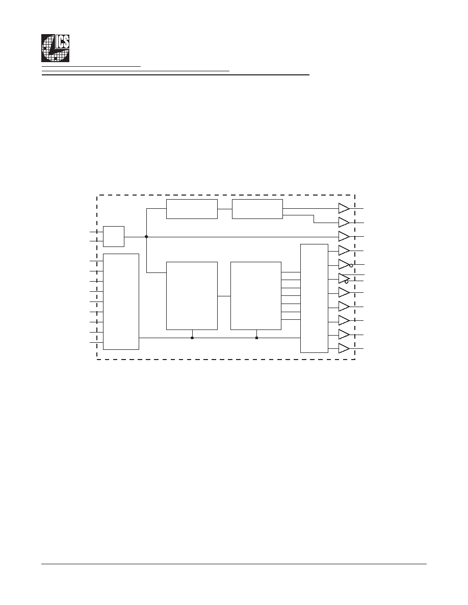
Block Diagram
PLL2
Frequency
Dividers
Programmable
Spread
PLL1
Programmable
Frequency
Dividers
STOP
Logic
ZCLK (1:0)
X1
X2
XTAL
CPU_STOP#
PCI_STOP#
SCLK
SEL24_48MHZ
SEL12_48MHz
PD#
FS (3:0)
MODE
SDATA
Control
Logic
PCICLK (5:0)
AGPCLK (1:0)
12_48MHZ
24_48MHZ
REF (2:0)
CPUCLKODC0
SRCCLKT
SRCCLKC
CPUCLKODT (1:0)
IOAPIC (1:0)
PCICLKF (1:0)
3
Integrated
Circuit
Systems, Inc.
ICS952703
Preliminary Product Preview
0813B--05/17/05
Pin Description
PIN # PIN NAME
PIN
TYPE
DESCRIPTION
1
VDDREF
PWR
Ref, XTAL power supply, nominal 3.3V
2
**FS0/REF0
I/O
Frequency select latch input pin / 14.318 MHz reference clock.
3
**FS1/REF1
I/O
Frequency select latch input pin / 14.318 MHz reference clock.
4
**Mode/REF2
I/O
Function select latch input pin, 0=Desktop Mode, 1=Mobile Mode / Ref clock output.
5
GNDREF
PWR
Ground pin for the REF outputs.
6
X1
IN
Crystal input, Nominally 14.318MHz.
7
X2
OUT
Crystal output, Nominally 14.318MHz
8
GNDZ
PWR
Ground pin for the ZCLK outputs
9
ZCLK0
OUT
3.3V Hyperzip clock output.
10
ZCLK1
OUT
3.3V Hyperzip clock output.
11
VDDZ
PWR
Power supply for ZCLK clocks, nominal 3.3V
12
SCLK
IN
Clock pin of I2C circuitry 5V tolerant
13
VDDPCI
PWR
Power supply for PCI clocks, nominal 3.3V
14
*FS2/PCICLK_F0
I/O
Frequency select latch input pin / 3.3V PCI free running clock output.
15
*FS3/PCICLK_F1
I/O
Frequency select latch input pin / 3.3V PCI free running clock output.
16
PCICLK0
OUT
PCI clock output.
17
PCICLK1
OUT
PCI clock output.
18
GNDPCI
PWR
Ground pin for the PCI outputs
19
VDDPCI
PWR
Power supply for PCI clocks, nominal 3.3V
20
PCICLK2
OUT
PCI clock output.
21
*(PCI_STOP#)PCICLK3
I/O
Stops all PCICLKs besides the PCICLK_F clocks at logic 0 level, when input low. This
input is activated by the MODE selection pin / PCI clock output.
22
*(CPU_STOP#)PCICLK4
I/O
Stops all CPUCLKs besides the CPUCLK_F clocks at logic 0 level, when input low. This
input is activated by the MODE selection pin / PCI clock output.
23
*(PD#)PCICLK5
I/O
Asynchronous active low input pin used to power down the device into a low power state /
PCI clock output.
24
GNDPCI
PWR
Ground pin for the PCI outputs
25
GND48
PWR
Ground pin for the 48MHz outputs
26
24_48MHz/SEL24_48#MHz**~
I/O
24/48MHz clock output / Latched select input for 24/48MHz output. 0=48MHz, 1 = 24MHz.
27
12_48MHz/SEL12_48#MHz*
I/O
12/48MHz clock output / Latched select input for 12/48MHz output. 0=48MHz, 1 = 12MHz.
28
AVDD48
PWR
Power for 24/48MHz outputs and fixed PLL core, nominal 3.3V
29
VDDAGP
PWR
Power supply for AGP clocks, nominal 3.3V
30
AGPCLK1
OUT
AGP clock output
31
AGPCLK0
OUT
AGP clock output
32
GNDAGP
PWR
Ground pin for the AGP outputs
33
SDATA
I/O
Data pin for I2C circuitry 5V tolerant
34
IREF
OUT
This pin establishes the reference current for the SRCCLK pairs. This pin requires a fixed
precision resistor tied to ground in order to establish the appropriate current.
35
AGND
PWR
Analog Ground pin for Core PLL
36
AVDD
PWR
3.3V Analog Power pin for Core PLL
37
CPUCLKODC0
OUT
"Complememtary" clocks of differential pair CPU outputs. These open drain outputs need
an external 1.5V pull-up.
38
CPUCLKODT0
OUT
True clock of differential pair CPU outputs. These open drain outputs need an external
1.5V pull-up.
39
GNDCPU
PWR
Ground pin for the CPU outputs
40
CPUCLKODT1
OUT
True clock of differential pair CPU outputs. These open drain outputs need an external
1.5V pull-up.
41
GND
PWR
Ground pin.
42
SRCCLKC
OUT
Complement clock of differential pair for S-ATA support.
+/- 300ppm accuracy required.
43
SRCCLKT
OUT
True clock of differential pair for S-ATA support.
+/- 300ppm accuracy required.
44
VDDSRC
PWR
Supply for SRC clocks, 3.3V nominal
45
GNDAPIC
PWR
Ground pin for the IOAPIC outputs.
46
IOAPIC0
OUT
IOAPIC clock outputs, norminal 2.5V.
47
IOAPIC1
OUT
IOAPIC clock outputs, norminal 2.5V.
48
VDDLAPIC
PWR
Power pin for the IOAPIC outputs. 2.5V.
* Internal Pull-Up Resistor ** Internal Pull-Down Resistor ~ 1.5X Drive Strength
4
Integrated
Circuit
Systems, Inc.
ICS952703
Preliminary Product Preview
0813B--05/17/05
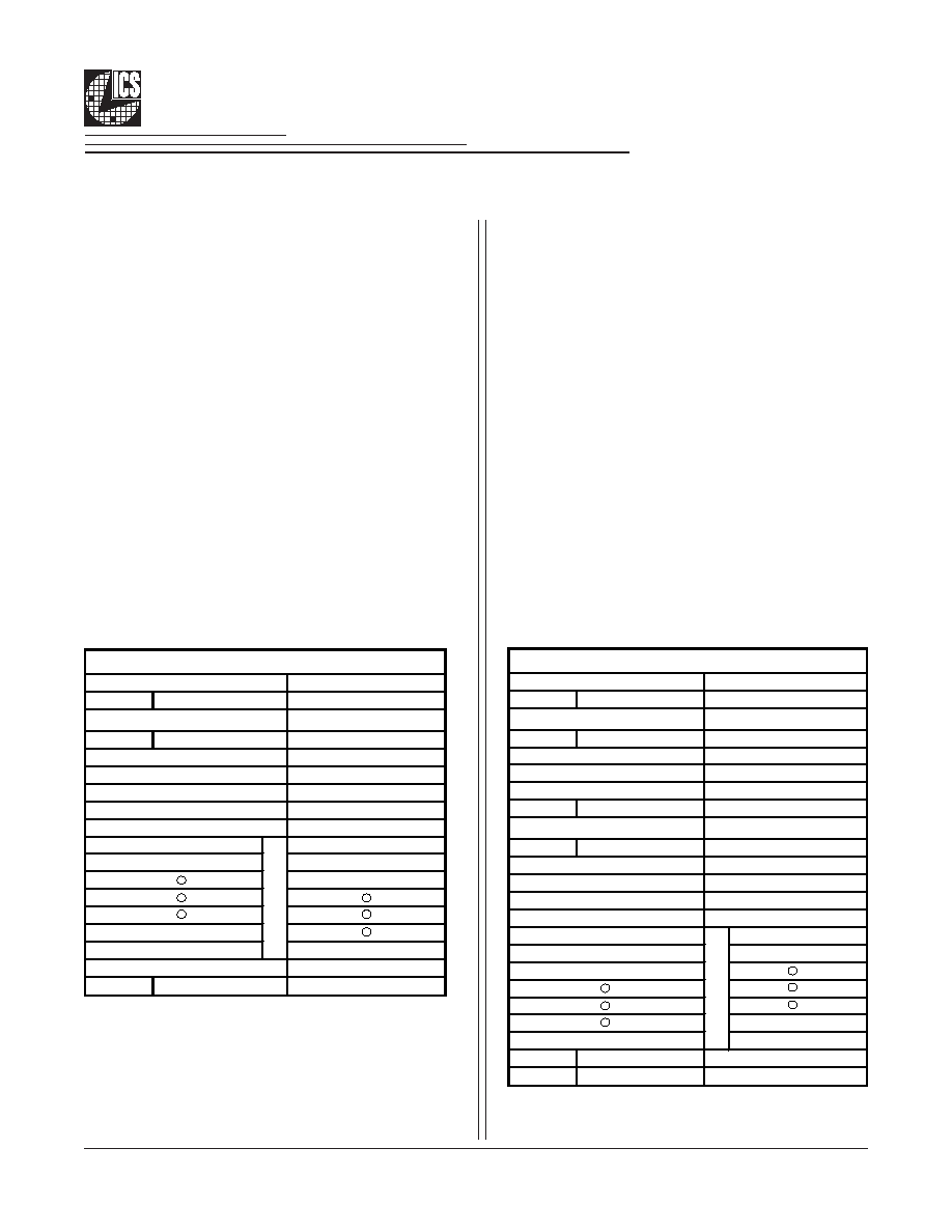
General SMBus serial interface information for the ICS952703
How to Write:
� Controller (host) sends a start bit.
� Controller (host) sends the write address D2
(H)
� ICS clock will
acknowledge
� Controller (host) sends the begining byte location = N
� ICS clock will
acknowledge
� Controller (host) sends the data byte count = X
� ICS clock will
acknowledge
� Controller (host) starts sending
Byte N through
Byte N + X -1
(see Note 2)
� ICS clock will
acknowledge each byte one at a time
� Controller (host) sends a Stop bit
How to Read:
� Controller (host) will send start bit.
� Controller (host) sends the write address D2
(H)
� ICS clock will
acknowledge
� Controller (host) sends the begining byte
location = N
� ICS clock will
acknowledge
� Controller (host) will send a separate start bit.
� Controller (host) sends the read address D3
(H)
� ICS clock will
acknowledge
� ICS clock will send the data byte count = X
� ICS clock sends
Byte N + X -1
� ICS clock sends
Byte 0 through byte X (if X
(H)
was written to byte 8)
.
� Controller (host) will need to acknowledge each
byte
� Controllor (host) will send a not acknowledge bit
� Controller (host) will send a stop bit
ICS (Slave/Receiver)
T
WR
ACK
ACK
ACK
ACK
ACK
P
stoP bit
X Byt
e
Index Block Write Operation
Slave Address D2
(H)
Beginning Byte = N
WRite
starT bit
Controller (Host)
Byte N + X - 1
Data Byte Count = X
Beginning Byte N
T
starT bit
WR
WRite
RT
Repeat starT
RD
ReaD
Beginning Byte N
Byte N + X - 1
N
Not acknowledge
P
stoP bit
Slave Address D3
(H)
Index Block Read Operation
Slave Address D2
(H)
Beginning Byte = N
ACK
ACK
Data Byte Count = X
ACK
ICS (Slave/Receiver)
Controller (Host)
X Byt
e
ACK
ACK
5
Integrated
Circuit
Systems, Inc.
ICS952703
Preliminary Product Preview
0813B--05/17/05
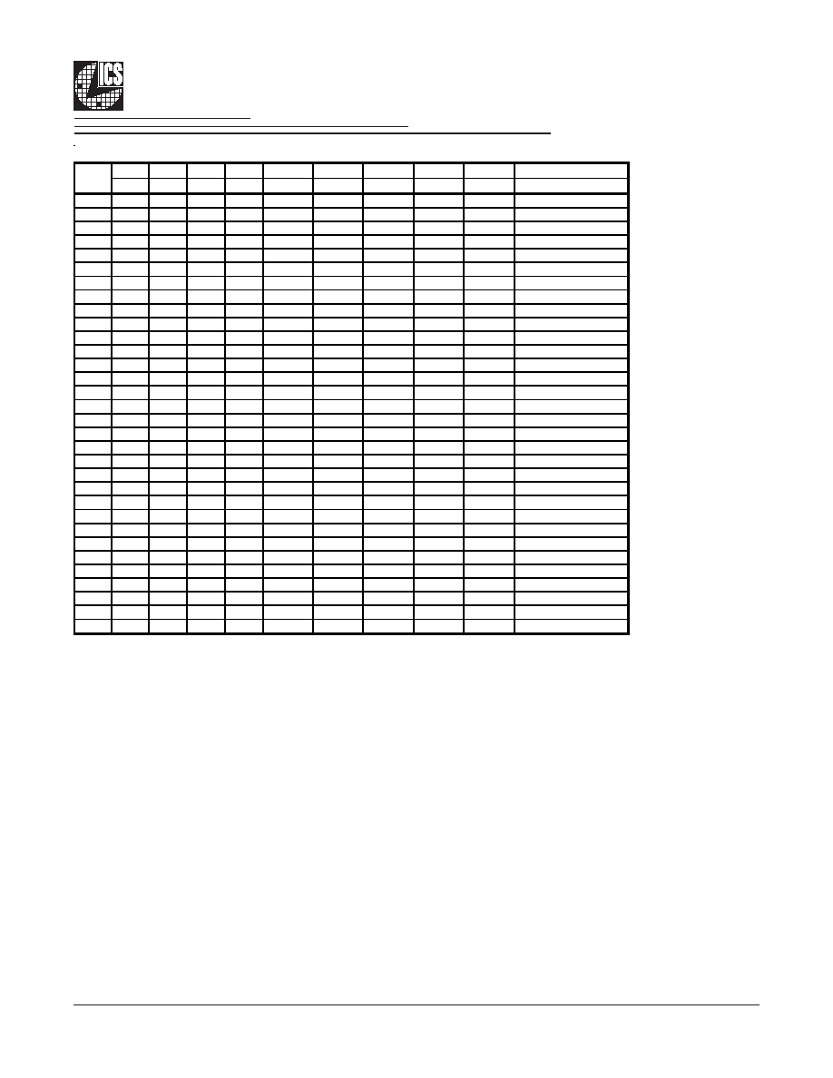
Table1: Frequency Selection Table
Bit3
Bit2
Bit1
Bit0
CPU
SRC
ZCLK
AG P
PCI
Spread %
FS3
FS2
FS1
FS0
MHz
MHz
MHz
MHz
MHz
0
0
0
0
0
200.00
100.00
133.33
66.66
33.33
0.5% down
0
0
0
0
1
200.01
100.00
133.34
66.67
33.33
0.35% c enter
0
0
0
1
0
200.97
100.00
133.98
66.99
33.49
0.35% c enter
0
0
0
1
1
190.11
100.00
126.74
63.37
31.69
0.35% c enter
0
0
1
0
0
100.00
100.00
133.33
66.66
33.33
0.5% down
0
0
1
0
1
100.00
100.00
133.34
66.67
33.33
0.35% c enter
0
0
1
1
0
100.99
100.00
134.66
67.33
33.66
0.35% c enter
0
0
1
1
1
95.00
100.00
126.66
63.33
31.67
0.35% c enter
0
1
0
0
0
166.66
100.00
133.33
66.66
33.33
0.5% down
0
1
0
0
1
166.65
100.00
133.32
66.66
33.33
0.35% c enter
0
1
0
1
0
161.59
100.00
129.27
64.64
32.32
0.35% c enter
0
1
0
1
1
151.97
100.00
121.57
60.79
30.39
0.35% c enter
0
1
1
0
0
133.33
100.00
133.33
66.66
33.33
0.5% down
0
1
1
0
1
133.34
100.00
133.34
66.67
33.33
0.35% c enter
0
1
1
1
0
133.98
100.00
133.98
66.99
33.49
0.35% c enter
0
1
1
1
1
126.66
100.00
126.66
63.33
31.67
0.35% c enter
1
0
0
0
0
206.02
100.00
137.35
68.67
34.34
0.35% c enter
1
0
0
0
1
210.00
100.00
140.00
70.00
35.00
0.35% c enter
1
0
0
1
0
214.06
100.00
142.70
71.35
35.68
0.35% c enter
1
0
0
1
1
217.90
100.00
145.27
72.63
36.32
0.35% c enter
1
0
1
0
0
103.01
100.00
137.35
68.67
34.34
0.35% c enter
1
0
1
0
1
105.00
100.00
140.00
70.00
35.00
0.35% c enter
1
0
1
1
0
106.99
100.00
142.65
71.33
35.66
0.35% c enter
1
0
1
1
1
109.01
100.00
145.35
72.68
36.34
0.35% c enter
1
1
0
0
0
164.66
100.00
131.73
65.86
32.93
0.35% c enter
1
1
0
0
1
167.91
100.00
134.33
67.17
33.58
0.35% c enter
1
1
0
1
0
171.22
100.00
136.98
68.49
34.24
0.35% c enter
1
1
0
1
1
174.38
100.00
139.50
69.75
34.88
0.35% c enter
1
1
1
0
0
137.32
100.00
137.32
68.66
34.33
0.35% c enter
1
1
1
0
1
140.00
100.00
140.00
70.00
35.00
0.35% c enter
1
1
1
1
0
142.67
100.00
142.67
71.34
35.67
0.35% c enter
1
1
1
1
1
145.33
100.00
145.33
72.66
36.33
0.35% c enter
Bit4