
Integrated
Circuit
Systems, Inc.
ICS951601
Preliminary Product Preview
0663A--10/01/02
Block Diagram
General Purpose Frequency Timing Generator
Pin Configuration
48-pin SSOP
*120K ohm pull-up to VDD on indicated inputs.
Recommended Application:
General Purpose Clock Generator
Output Features:
·
17 - PCI clocks selectable,
either 33.33MHz or 66.6MHz @ 3.3V
·
1 - 48MHz @ 3.3V
·
1 - REF @ 3.3V, 14.318MHz.
Features:
·
Programable Spread spectrum precentage for EMI control
·
Uses external 14.318MHz crystal
·
Select pins for frequency select
Key Specifications:
·
PCI PCI output skew within same bank @ 33MHz:
<170ps
·
PCI PCI output skew within same bank@ 66MHz:
<340ps
·
Cycle to Cycle Jitter PCI @ 33MHz: <200ps
·
Cycle to Cycle Jitter PCI @ 66MHz: <200ps
·
Cycle to Cycle Jitter 48MHz: <350ps
·
Cycle to Cycle Jitter REF: <500ps
·
Slew Rate: 1.5 - 4 V/ns. (PCI spec.)
PLL2
PLL1
Spread
Spectrum
48MHz
PCI1A (7:0)
PCI2A (2:0)
PCI1B (2:0)
PCI2B (2:0)
8
3
3
3
X1
X2
XTAL
OSC
PCI
DIVDER
PCI
DIVDER
PCI
DIVDER
PCI
DIVDER
SDATA
SCLK
SELA (2:1)
SELB (2:1)
SPREAD
Control
Logic
Config.
Reg.
REF0
REF0
VDD
X1
X2
GND
SDATA
SCLK
GNDA
VDDA
SEL1A
PCI1A_0
PCI1A_1
VDD33
GND
PCI1A_2
PCI1A_3
GND
VDD33
PC1A_4
PCI1A_5
VDD33
GND
PCI1A_5
PCI1A_7I
48MHz
GND
VDD48
SPREAD
VDDA
GNDA
SEL2B
PCI2B_2
PCI2B_1
GND
VDD66
PCI2B_0
SEL2A
PCI2A_2
PCI2A_1
VDD2A
GND
PCI2A_0
SEL1B
PCI1B_2
PCI1B_1
GND
VDD1B
PCI1B_0
ICS951601
1
2
3
4
5
6
7
8
9
10
11
12
13
14
15
16
17
18
19
20
21
22
23
24
48
47
46
45
44
43
42
41
40
39
38
37
36
35
34
33
32
31
30
29
28
27
26
25
Power Groups:
VDDA = Analog Power
GNDA = Analog Ground
PRODUCT PREVIEW documents contain information on new products in the sampling or preproduction phase of development. Characteristic data and other specifications are subject to
change without notice.
2
ICS951601
Preliminary Product Preview
0663A--10/01/02
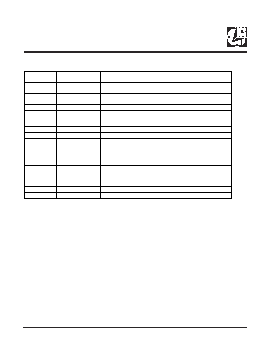
Pin Descriptions
Pin number
Pin name
Type
Description
1
REF0
OUT
Reference output
2, 13, 18, 21, 26,
33, 38, 46
VDD
PWR
3.3V Power supply
3
X1
IN
Crystal input,nominally 14.318MHz.
4
X2
OUT
Crystal output, nominally 14.318MHz.
9, 44
VDDA
PWR
Analog 3.3V Power supply
10, 30, 36, 42
SELxx
IN
Real time PCI output frequency selection pins
5, 14, 17, 22, 27,
32, 39, 47
GND
PWR
Ground pins
6
SDATA
I/O
Data pin for I
2
C circuitry 5V tolerant
7
SCLK
IN
Clock input of I
2
C input
8, 43
GNDA
PWR
Analog ground pins
24, 23, 20, 19,
16, 15, 12, 11,
PCI1A (7:0)
OUT
PCI clock outputs, selectable to be either
33.33 or 66.66MHz at 3.3V.
29, 28, 25
PCI1B (2:0)
OUT
PCI clock outputs, selectable to be either
33.33 or 66.66MHz at 3.3V.
35, 34, 31
PCI2A (2:0)
OUT
PCI clock outputs, selectable to be either
33.33 or 66.66MHz at 3.3V.
41, 40, 37
PCI2B (2:0)
OUT
PCI clock outputs, selectable to be either
33.33 or 66.66MHz at 3.3V.
45
SPREAD
IN
Enables Spread Spectrum, default is on.
48
48MHz
OUT
Fixed 48MHz clock output for USB.

3
ICS951601
Preliminary Product Preview
0663A--10/01/02
1.
The ICS clock generator is a slave/receiver, I
2
C component. It can read back the data stored in the latches for
verification. Read-Back will support Intel PIIX4 "Block-Read" protocol.
2.
The data transfer rate supported by this clock generator is 100K bits/sec or less (standard mode)
3.
The input is operating at 3.3V logic levels.
4.
The data byte format is 8 bit bytes.
5.
To simplify the clock generator I
2
C interface, the protocol is set to use only "Block-Writes" from the controller.
The bytes must be accessed in sequential order from lowest to highest byte with the ability to stop after any
complete byte has been transferred. The Command code and Byte count shown above must be sent, but the
data is ignored for those two bytes. The data is loaded until a Stop sequence is issued.
6.
At power-on, all registers are set to a default condition, as shown.
General I
2
C serial interface information
The information in this section assumes familiarity with I
2
C programming.
For more information, contact ICS for an I
2
C programming application note.
How to Write:
· Controller (host) sends a start bit.
· Controller (host) sends the write address D2
(H)
· ICS clock will acknowledge
· Controller (host) sends a dummy command code
· ICS clock will acknowledge
· Controller (host) sends a dummy byte count
· ICS clock will acknowledge
· Controller (host) starts sending first byte (Byte 0)
through byte 5
· ICS clock will acknowledge each byte one at a time.
· Controller (host) sends a Stop bit
How to Read:
· Controller (host) will send start bit.
· Controller (host) sends the read address D3
(H)
· ICS clock will acknowledge
· ICS clock will send the byte count
· Controller (host) acknowledges
· ICS clock sends first byte (Byte 0) through byte 5
· Controller (host) will need to acknowledge each byte
· Controller (host) will send a stop bit
Notes:
Controller (Host)
ICS (Slave/Receiver)
Start Bit
Address
D3
(H)
ACK
Byte Count
ACK
Byte 0
ACK
Byte 1
ACK
Byte 2
ACK
Byte 3
ACK
Byte 4
ACK
Byte 5
ACK
Stop Bit
How to Read:
Controller (Host)
ICS (Slave/Receiver)
Start Bit
Address
D2
(H)
ACK
Dummy Command Code
ACK
Dummy Byte Count
ACK
Byte 0
ACK
Byte 1
ACK
Byte 2
ACK
Byte 3
ACK
Byte 4
ACK
Byte 5
ACK
Stop Bit
How to Write:
4
ICS951601
Preliminary Product Preview
0663A--10/01/02
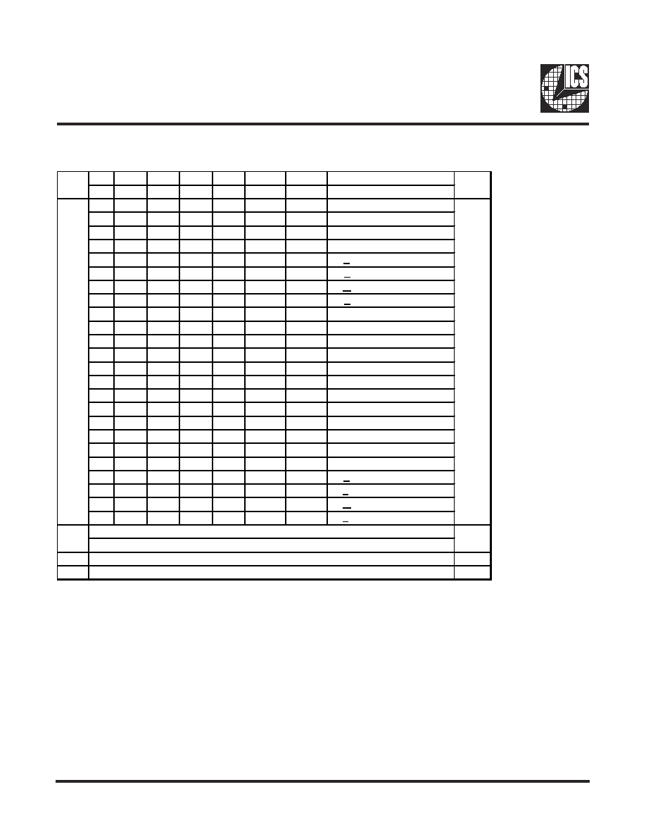
Byte 0: Functionality and frequency select register (Default = 0)
Serial Configuration Command Bitmap
Bit2 Bit7
Bit6
Bit5
Bit4
66MHZ 33MHz
FEATURES
FS4 FS3
FS2
FS1
FS0
0
0
0
0
0
66
33
-0.25 % down spread
0
0
0
0
1
66
33
-0.5 % down spread
0
0
0
1
0
66
33
-1.0 % down spread
0
0
0
1
1
66
33
-1.5 % down spread
0
0
1
0
0
66
33
+ 0.25 % center spread
0
0
1
0
1
66
33
+0.5 % center spread
0
0
1
1
0
66
33
+ 1.0 % center spread
0
0
1
1
1
66.6
33.3
+1.5 % center spread
0
1
0
0
0
67.32
33.66
2% over-clocking
0
1
0
0
1
68.64
34.32
4% over-clocking
0
1
0
1
0
69.96
34.98
6% over-clocking
0
1
0
1
1
72.6
36.3
10% over-clocking
0
1
1
0
0
65.27
32.63
2% under- clocking
0
1
1
0
1
63.96
31.97
2% under- clocking
0
1
1
1
0
62.6
31.3
2% under- clocking
0
1
1
1
1
60
30
2% under- clocking
1
0
0
0
0
66.6
33.3
-1.4 % down spread
1
0
0
0
1
66.6
33.3
-1.6 % down spread
1
0
0
1
0
66.6
33.3
-1.8 % down spread
1
0
0
1
1
66.6
33.3
-2.0 % down spread
1
0
1
0
0
66.6
33.3
+ 1.4 % center spread
1
0
1
0
1
66.6
33.3
+ 1.6 % center spread
1
0
1
1
0
66.6
33.3
+ 1.8 % center spread
1
0
1
1
1
66.6
33.3
+ 2.0 % center spread
Bit1
0-Normal 1-Spread spectrum Enabled
0
Bit0
0-Running 1-Tristate all outputs
0
Bit
PWD
00000
Bit
2,7:4
Bit3
0
0-Frequency and Spread is seleced by hardware select. Latched input
1-Frequency is seleced by Bit2, 7:4
5
ICS951601
Preliminary Product Preview
0663A--10/01/02
Byte 1: PCI1A Stop Clocks Register
(1 = enable, 0 = disable)
Byte 2: PCI2A Stop Clocks
Register (1 = enable, 0 = disable)
Byte 3: PCI2B Stop Clocks Register
(1 = enable, 0 = disable)
Byte 4: Reserved Register
(1 = enable, 0 = disable)
t
i
B
#
n
i
P
D
W
P
n
o
i
t
p
i
r
c
s
e
D
7
t
i
B
4
2
1
7
_
A
1
I
C
P
6
t
i
B
3
2
1
6
_
A
1
I
C
P
5
t
i
B
0
2
1
5
_
A
1
I
C
P
4
t
i
B
9
1
1
4
_
A
1
I
C
P
3
t
i
B
6
1
1
3
_
A
1
I
C
P
2
t
i
B
5
1
1
2
_
A
1
I
C
P
1
t
i
B
2
1
1
1
_
A
1
I
C
P
0
t
i
B
1
1
1
0
_
A
1
I
C
P
t
i
B
#
n
i
P
D
W
P
n
o
i
t
p
i
r
c
s
e
D
7
t
i
B
6
3
1
2
_
A
2
I
C
P
6
t
i
B
4
3
1
1
_
A
2
I
C
P
5
t
i
B
1
3
1
0
_
A
2
I
C
P
4
t
i
B
9
2
1
2
_
B
1
I
C
P
3
t
i
B
8
2
1
1
_
B
1
I
C
P
2
t
i
B
5
2
1
0
_
B
1
I
C
P
1
t
i
B
-
X
d
e
v
r
e
s
e
R
0
t
i
B
-
X
d
e
v
r
e
s
e
R
t
i
B
#
n
i
P
D
W
P
n
o
i
t
p
i
r
c
s
e
D
7
t
i
B
1
4
1
2
_
B
2
I
C
P
6
t
i
B
0
4
1
1
_
B
2
I
C
P
5
t
i
B
7
3
1
0
_
B
2
I
C
P
4
t
i
B
-
X
d
e
v
r
e
s
e
R
3
t
i
B
-
X
d
e
v
r
e
s
e
R
2
t
i
B
-
X
d
e
v
r
e
s
e
R
1
t
i
B
-
X
d
e
v
r
e
s
e
R
0
t
i
B
-
X
d
e
v
r
e
s
e
R
t
i
B
#
n
i
P
D
W
P
n
o
i
t
p
i
r
c
s
e
D
7
t
i
B
8
4
1
z
H
M
8
4
6
t
i
B
1
1
0
F
E
R
5
t
i
B
-
X
d
e
v
r
e
s
e
R
4
t
i
B
-
X
d
e
v
r
e
s
e
R
3
t
i
B
-
X
d
e
v
r
e
s
e
R
2
t
i
B
-
X
d
e
v
r
e
s
e
R
1
t
i
B
-
X
d
e
v
r
e
s
e
R
0
t
i
B
-
X
d
e
v
r
e
s
e
R
Byte 5: Latched Input Read Back Register
(1= enable, 0 = disable)
t
i
B
#
n
i
P
D
W
P
n
o
i
t
p
i
r
c
s
e
D
7
t
i
B
-
X
B
2
L
E
S
6
t
i
B
-
X
B
1
L
E
S
5
t
i
B
-
X
A
2
L
E
S
4
t
i
B
-
X
A
1
L
E
S
3
t
i
B
-
X
d
e
v
r
e
s
e
R
2
t
i
B
-
X
d
e
v
r
e
s
e
R
1
t
i
B
-
X
d
e
v
r
e
s
e
R
0
t
i
B
-
X
d
e
v
r
e
s
e
R
Byte 6: Reserved for Byte Count Register
(1= enable, 0 = disable)
t
i
B
#
n
i
P
D
W
P
n
o
i
t
p
i
r
c
s
e
D
7
t
i
B
-
0
d
a
e
r
r
o
f
d
e
v
r
e
s
e
R
t
n
u
o
c
e
t
y
b
6
t
i
B
-
0
d
e
v
r
e
s
e
R
5
t
i
B
-
0
d
e
v
r
e
s
e
R
4
t
i
B
-
0
d
e
v
r
e
s
e
R
3
t
i
B
-
0
d
e
v
r
e
s
e
R
2
t
i
B
-
1
d
e
v
r
e
s
e
R
1
t
i
B
-
1
d
e
v
r
e
s
e
R
0
t
i
B
-
0
d
e
v
r
e
s
e
R
Note: PWD = Power-Up Default