Integrated
Circuit
Systems, Inc.
ICS9248- 185
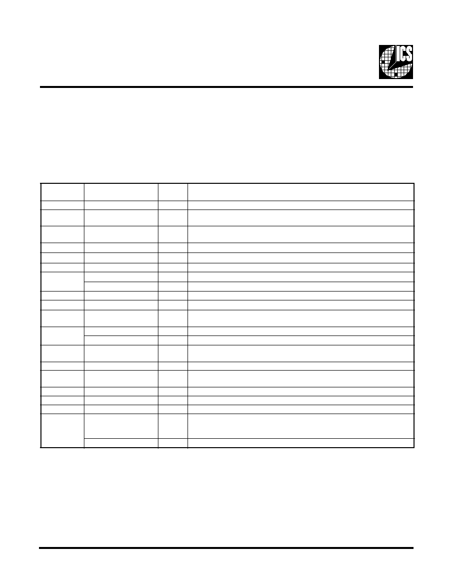
Block Diagram
Pentium is a trademark of Intel Corporation
I
2
C is a trademark of Philips Corporation
Frequency Generator & Integrated Buffers for PENTIUM/Pro
TM
& K6
9248-185 RevC - 10/25/01
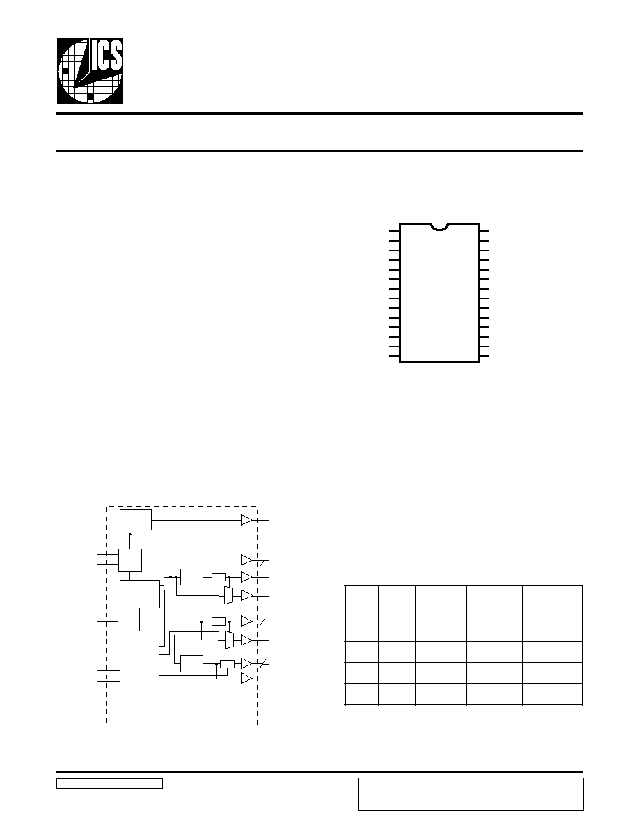
Pin Configuration
28-Pin SSOP/TSSOP
* Internal Pull-up Resistor of 120K to VDD
1. These pin will have 2X drive strength
2. FS1 is a pull down
Recommended Application:
VIA PM133 chipset
Output Features:
·
2 - CPUs @ 2.5V
·
5 - SDRAM @ 3.3V
·
3 - PCI @ 3.3V,
·
1 - 48MHz, @ 3.3V fixed.
·
2 - REF @ 3.3V, 14.318MHz.
Features:
·
Up to 133MHz frequency support
·
Support power management: PCI_STOP & CLK_STOP
·
Spread spectrum for EMI control (-0.5% down spread).
·
Uses external 14.318MHz crystal
·
FS pins for frequency select
Key Specifications:
·
CPU PCI Skew: 1-4ns
·
PCI PCI Skew: ±500ps
·
CPU CPU Skew: ±175ps
·
CPU Jitter: 250ps (cyc-cyc)
·
PCI Jitter: 500ps (cyc-cyc)
BUFFER_IN
PLL2
PLL1
Spread
Spectrum
48MHz
CPUCLK1
SDRAM (4:1)
PCICLK (1:0)
2
2
4
SDRAM0/_F
CPUCLK0/_F
PCICLK_F
X1
X2
XTAL
OSC
CPU
DIVDER
PCI
DIVDER
Stop
Stop
Stop
PCI_STOP#
CLK_STOP#
FS (1:0)
Control
Logic
Config.
Reg.
REF (1:0)
Frequency Select
VDD
REF0
GND
X1
X2
VDDPCI
*PCICLK_F
GND
FS1/PCICLK0
BUFFER_IN
PCICLK1
PCI_STOP#
GND
*FS0/48MHz
1
1, 2
1
REF1/FREE_SEL*
VDDL
CPUCLK0/_F
CPUCLK1
GND
CLK_STOP#
SDRAM0/_F
SDRAM1
SDRAM2
GND
VDDSDR
SDRAM3
SDRAM4
VDD48
1
ICS9248-185
1
2
3
4
5
6
7
8
9
10
11
12
13
14
28
27
26
25
24
23
22
21
20
19
18
17
16
15
1
S
F
0
S
F
K
L
C
U
P
C
K
L
C
I
C
P
n
w
o
D
d
a
e
r
p
S
0
0
6
6
.
6
6
3
3
.
3
3
%
5
.
0
-
0
1
0
0
.
0
0
1
3
3
.
3
3
%
5
.
0
-
1
0
0
0
.
7
9
3
3
.
2
3
%
5
.
0
-
1
1
3
3
.
3
3
1
3
3
.
3
3
%
5
.
0
-
ICS reserves the right to make changes in the device data identified in
this publication without further notice. ICS advises its customers to
obtain the latest version of all device data to verify that any
information being relied upon by the customer is current and accurate.
2
ICS9248- 185
Pin Descriptions
Notes:
1:
Internal Pull-up Resistor of 120K to 3.3V on indicated inputs
2:
Bidirectional input/output pins, input logic levels are latched at internal power-on-reset. Use 10Kohm resistor
to program logic Hi to VDD or GND for logic low.
General Description
The ICS9248-185 is the single chip clock solution for Notebook designs using the 440BX or the VIA Apollo Pro 133 style
chipset. It provides all necessary clock signals for such a system. The ICS9248-185 provides CPU and PCI clocks with
continous spread spectrum. The ICS9248-185 employs a proprietary closed loop design, which tightly controls the percentage
of spreading over process and temperature variations.
N
I
P
R
E
B
M
U
N
E
M
A
N
N
I
P
E
P
Y
T
N
O
I
T
P
I
R
C
S
E
D
,
8
1
,
5
1
,
6
,
1
D
D
V
R
W
P
V
3
.
3
l
a
n
i
m
o
n
,
y
l
p
p
u
s
r
e
w
o
P
2
0
F
E
R
T
U
O
r
e
f
f
u
b
R
E
G
N
O
R
T
S
e
h
t
s
i
t
u
p
t
u
o
F
E
R
s
i
h
T
.
k
c
o
l
c
e
c
n
e
r
e
f
e
r
z
h
M
8
1
3
.
4
1
s
d
a
o
l
S
U
B
A
S
I
r
o
f
,
3
1
,
8
,
3
4
2
,
9
1
D
N
G
R
W
P
d
n
u
o
r
G
4
1
X
N
I
2
X
m
o
r
f
r
o
t
s
i
s
e
r
k
c
a
b
d
e
e
f
d
n
a
)
F
p
6
3
(
p
a
c
d
a
o
l
l
a
n
r
e
t
n
i
s
a
h
,t
u
p
n
i
l
a
t
s
y
r
C
5
2
X
T
U
O
.
z
H
M
8
1
3
.
4
1
y
l
l
a
n
i
m
o
n
,t
u
p
t
u
o
l
a
t
s
y
r
C
7
F
_
K
L
C
I
C
P
T
U
O
.t
n
e
m
e
g
a
n
a
m
r
e
w
o
p
r
o
f
#
P
O
T
S
_
I
C
P
y
b
d
e
t
c
e
f
f
a
t
o
n
k
c
o
l
c
I
C
P
g
n
i
n
n
u
r
e
e
r
F
9
1
S
F
2
,
1
N
I
.t
u
p
n
I
d
e
h
c
t
a
L
.
n
i
p
t
c
e
l
e
s
y
c
n
e
u
q
e
r
F
0
K
L
C
I
C
P
T
U
O
)
y
l
r
a
e
U
P
C
(
w
e
k
s
s
n
4
-
1
h
t
i
w
s
k
c
o
l
c
U
P
C
o
t
s
u
o
n
o
r
h
c
n
y
S
.t
u
p
t
u
o
k
c
o
l
c
I
C
P
0
1
N
I
R
E
F
F
U
B
N
I
.
s
t
u
p
t
u
o
M
A
R
D
S
r
o
f
s
r
e
f
f
u
B
t
u
o
n
a
F
o
t
t
u
p
n
I
1
1
1
K
L
C
I
C
P
T
U
O
)
y
l
r
a
e
U
P
C
(
w
e
k
s
s
n
4
-
1
h
t
i
w
s
k
c
o
l
c
U
P
C
o
t
s
u
o
n
o
r
h
c
n
y
S
.t
u
p
t
u
o
k
c
o
l
c
I
C
P
2
1
#
P
O
T
S
_
I
C
P
N
I
w
o
l
t
u
p
n
i
n
e
h
w
,l
e
v
e
l
0
c
i
g
o
l
t
a
s
k
c
o
l
c
K
L
C
I
C
P
s
t
l
a
H
)
0
=
E
D
O
M
,
e
d
o
m
e
l
i
b
o
m
n
I
(
4
1
0
S
F
2
,
1
N
I
t
u
p
n
I
d
e
h
c
t
a
L
.
n
i
p
t
c
e
l
e
s
y
c
n
e
u
q
e
r
F
z
H
M
8
4
T
U
O
k
c
o
l
c
t
u
p
t
u
o
z
H
M
8
4
,
0
2
,
7
1
,
6
1
1
2
)
1
:
4
(
M
A
R
D
S
T
U
O
n
i
p
N
I
R
E
F
F
U
B
m
o
r
f
s
t
u
p
t
u
o
r
e
f
f
u
B
t
u
o
n
a
F
,
s
t
u
p
t
u
o
k
c
o
l
c
M
A
R
D
S
.
)
t
e
s
p
i
h
c
y
b
d
e
l
l
o
r
t
n
o
c
(
2
2
F
_
/
0
M
A
R
D
S
T
U
O
L
E
S
_
E
E
R
F
n
o
g
n
i
d
n
e
p
e
d
e
l
b
a
p
p
o
t
s
r
o
M
A
R
D
S
g
n
i
n
n
u
r
e
e
r
f
r
e
h
t
i
E
3
2
#
P
O
T
S
_
K
L
C
N
I
l
e
v
e
l
"
0
"
c
i
g
o
l
t
a
s
M
A
R
D
S
&
,
s
K
L
C
U
P
C
s
t
l
a
h
t
u
p
n
i
s
u
o
n
o
r
h
c
n
y
s
a
s
i
h
T
.
w
o
l
n
e
v
i
r
d
n
e
h
w
5
2
1
K
L
C
U
P
C
T
U
O
L
D
D
V
y
b
d
e
r
e
w
o
p
,t
u
p
t
u
o
k
c
o
l
c
U
P
C
6
2
F
_
/
0
K
L
C
U
P
C
T
U
O
L
E
S
_
E
E
R
F
n
o
g
n
i
d
n
e
p
e
d
e
l
b
a
p
p
o
t
s
r
o
K
L
C
U
P
C
g
n
i
n
n
u
r
e
e
r
f
r
e
h
t
i
E
7
2
L
D
D
V
R
W
P
V
5
.
2
s
k
c
o
l
c
U
P
C
r
o
f
y
l
p
p
u
S
8
2
L
E
S
_
E
E
R
F
N
I
r
o
g
n
i
n
n
u
r
e
e
r
f
r
e
h
t
i
e
e
b
o
t
F
_
/
0
M
A
R
D
S
d
n
a
F
_
/
0
K
L
C
U
P
C
s
t
c
e
l
e
S
e
v
o
b
a
e
h
t
w
o
l
)
0
(
o
t
t
e
s
s
i
L
E
S
_
E
E
R
F
n
e
h
W
.
#
P
O
T
S
_
K
L
C
y
b
e
l
b
a
p
p
o
t
s
.
e
l
b
a
p
p
o
t
s
e
r
a
s
k
c
o
l
c
e
h
t
,
h
g
i
h
)
1
(
o
t
t
e
s
n
e
h
w
-
g
n
i
n
n
u
r
e
e
r
f
e
r
a
s
k
c
o
l
c
1
F
E
R
T
U
O
.
k
c
o
l
c
e
c
n
e
r
e
f
e
r
z
H
M
8
1
3
.
4
1
3
ICS9248- 185
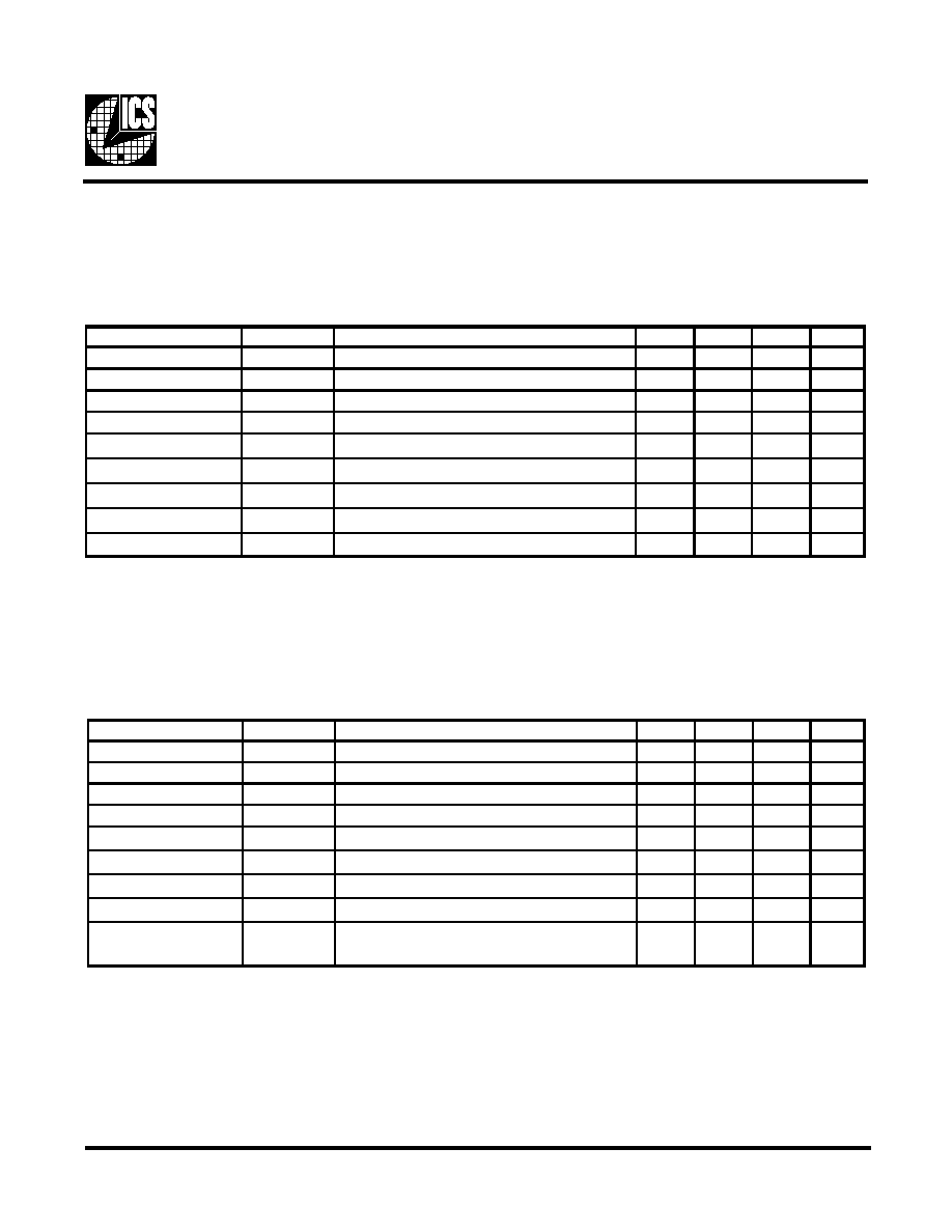
Electrical Characteristics - Input/Supply/Common Output Parameters
T
A
= 0 - 70C; Supply Voltage V
DD
= 3.3 V +/-5%, V
DDL
= 2.5 V +/-5% (unless otherwise stated)
PARAMETER
SYMBOL
CONDITIONS
MIN
TYP
MAX
UNITS
Input High Voltage
V
IH
2
V
DD
+0.3
V
Input Low Voltage
V
IL
V
SS
-0.3
0.8
V
C
L
= 30 pF; Select @ 66MHz
63
150
C
L
= 30 pF; Select @ 100MHz
67
170
C
L
= 30 pF; Select @ 133MHz
73
180
Powerdown Current
I
DDPD
CL = 0 pF; Input address VDD or GND
600
µ
A
Input Frequency
F
i
V
DD
= 3.3 V
12
14.318
16
MHz
Input Capacitance
1
C
IN
Logic Inputs
5
pF
C
INX
X1 & X2 pins
27
36
45
pF
Clk Stabilization
1
T
STAB
From V
DD
= 3.3 V to 1% target Freq.
5.5
ms
Skew
1
t
CPU-PCI1
V
T
= 1.5 V
1
28
4
ns
1
Guaranteed by design, not 100% tested in production.
mA
Operating Supply
Current
I
DD3.3OP
Absolute Maximum Ratings
Supply Voltage . . . . . . . . . . . . . . . . . . . . . . . . . . . 5.5 V
Logic Inputs . . . . . . . . . . . . . . . . . . . . . . . . . . . . . GND 0.5 V to V
DD
+0.5 V
Ambient Operating Temperature . . . . . . . . . . . . 0°C to +70°C
Case Temperature . . . . . . . . . . . . . . . . . . . . . . . . 115°C
Storage Temperature . . . . . . . . . . . . . . . . . . . . . . 65°C to +150°C
Stresses above those listed under Absolute Maximum Ratings may cause permanent damage to the device. These ratings are stress
specifications only and functional operation of the device at these or any other conditions above those listed in the operational
sections of the specifications is not implied. Exposure to absolute maximum rating conditions for extended periods may affect
product reliability.
4
ICS9248- 185
Electrical Characteristics - CPU
T
A
= 0 - 70C; V
DD
= 3.3 V +/-5%; C
L
= 20 pF
PARAMETER
SYMBOL
CONDITIONS
MIN
TYP
MAX UNITS
Output High Voltage
V
OH2A
I
OH
= -20 mA
2.4
2.85
V
Output Low Voltage
V
OL2A
I
OL
= 12 mA
0.31
0.4
V
Output High Current
I
OH2A
V
OH
= 2.0 V
-45
-27
mA
Output Low Current
I
OL2A
V
OL
= 0.8 V
22
29
mA
Rise Time
1
t
r2A
V
OL
= 0.4 V, V
OH
= 2.4 V
0.9
1.6
ns
Fall Time
1
t
f2A
V
OH
= 2.4 V, V
OL
= 0.4 V
1
1.6
ns
Duty Cycle
1
d
t2A
V
T
= 1.5 V
45
50
55
%
Skew window
1
t
sk2A
V
T
= 1.5 V
35
175
ps
Jitter, Cycle-to-cycle
1
t
jcyc-cyc2A
V
T
= 1.5 V Dram not running, CPU=66.6MHz
123
150
ps
Jitter, Cycle-to-cycle
1
t
jcyc-cyc2A
V
T
= 1.5 V Dram running
119
250
ps
1
Guaranteed by design, not 100% tested in production.
Electrical Characteristics - CPU
T
A
= 0 - 70C; VDDL= 2.5V, +/-5%; C
L
= 20 pF
PARAMETER
SYMBOL
CONDITIONS
MIN
TYP
MAX UNITS
Output High Voltage
V
OH2A
I
OH
= -20 mA
2
2.3
V
Output Low Voltage
V
OL2A
I
OL
= 12 mA
0.31
0.4
V
Output High Current
I
OH2A
V
OH
= 2.0 V
-39
-21
mA
Output Low Current
I
OL2A
V
OL
= 0.8 V
22
26
mA
Rise Time
1
t
r2A
V
OL
= 0.4 V, V
OH
= 2.0 V
0.96
1.6
ns
Fall Time
1
t
f2A
V
OH
= 2.0 V, V
OL
= 0.4 V
1.06
1.6
ns
Duty Cycle
1
d
t2A
V
T
= 1.25 V
45
50.3
55
%
Skew window
1
t
sk2A
V
T
= 1.25 V
35
175
ps
Jitter, Cycle-to-cycle
1
t
jcyc-cyc2A
V
T
= 1.25 V Dram not running
123
150
ps
Jitter, Cycle-to-cycle
1
t
jcyc-cyc2A
V
T
= 1.25 V Dram running
119
250
ps
1
Guaranteed by design, not 100% tested in production.
5
ICS9248- 185
Electrical Characteristics - PCI
T
A
= 0 - 70C; V
DD
= 3.3 V , VDDL = 2.5V, +/-5%; C
L
= 30 pF
PARAMETER
SYMBOL
CONDITIONS
MIN
TYP
MAX UNITS
Output High Voltage
V
OH1
I
OH
= -18 mA
2.4
3
V
Output Low Voltage
V
OL1
I
OL
= 9.4 mA
0.2
0.4
V
Output High Current
I
OH1
V
OH
= 2.0 V
-62
-33
mA
Output Low Current
I
OL1
V
OL
= 0.8 V
38
43
mA
Rise Time
1
t
r1
V
OL
= 0.4 V, V
OH
= 2.4 V
1.51
2
ns
Fall Time
1
t
f1
V
OH
= 2.4 V, V
OL
= 0.4 V
1.47
2
ns
Duty Cycle
1
d
t1
V
T
= 1.5 V
45
50.1
55
%
Skew window
1
t
sk1
V
T
= 1.5 V
58
500
ps
Jitter, Cycle to cycle
t
cycle
V
T
= 1.5 V
145
500
ps
1
Guaranteed by design, not 100% tested in production.
Electrical Characteristics - SDRAM
T
A
= 0 - 70C; V
DD
= 3.3 V, VDDL= 2.50V, +/-5%; C
L
= 30 pF
PARAMETER
SYMBOL
CONDITIONS
MIN
TYP
MAX UNITS
Output High Voltage
V
OH3
I
OH
= -28 mA
2.4
3
V
Output Low Voltage
V
OL3
I
OL
= 19 mA
0.3
0.4
V
Output High Current
I
OH3
V
OH
= 2.0 V
-69
-46
mA
Output Low Current
I
OL3
V
OL
= 0.8 V
32
42
mA
Rise Time
1
T
r3
V
OL
= 0.4 V, V
OH
= 2.4 V
1.07
1.3
ns
Fall Time
1
T
f3
V
OH
= 2.4 V, V
OL
= 0.4 V
1.3
2
ns
Duty Cycle
1
D
t3
V
T
= 1.5 V
45
50.8
55
%
Skew window
1
T
sk3
V
T
= 1.5 V
104
250
ps
Propagation Time
1
(Buffer In to output)
T
sk3
V
T
= 1.5 V
5
ns
1
Guaranteed by design, not 100% tested in production.