Integrated
Circuit
Systems, Inc.
ICS91857
0494C--08/15/05
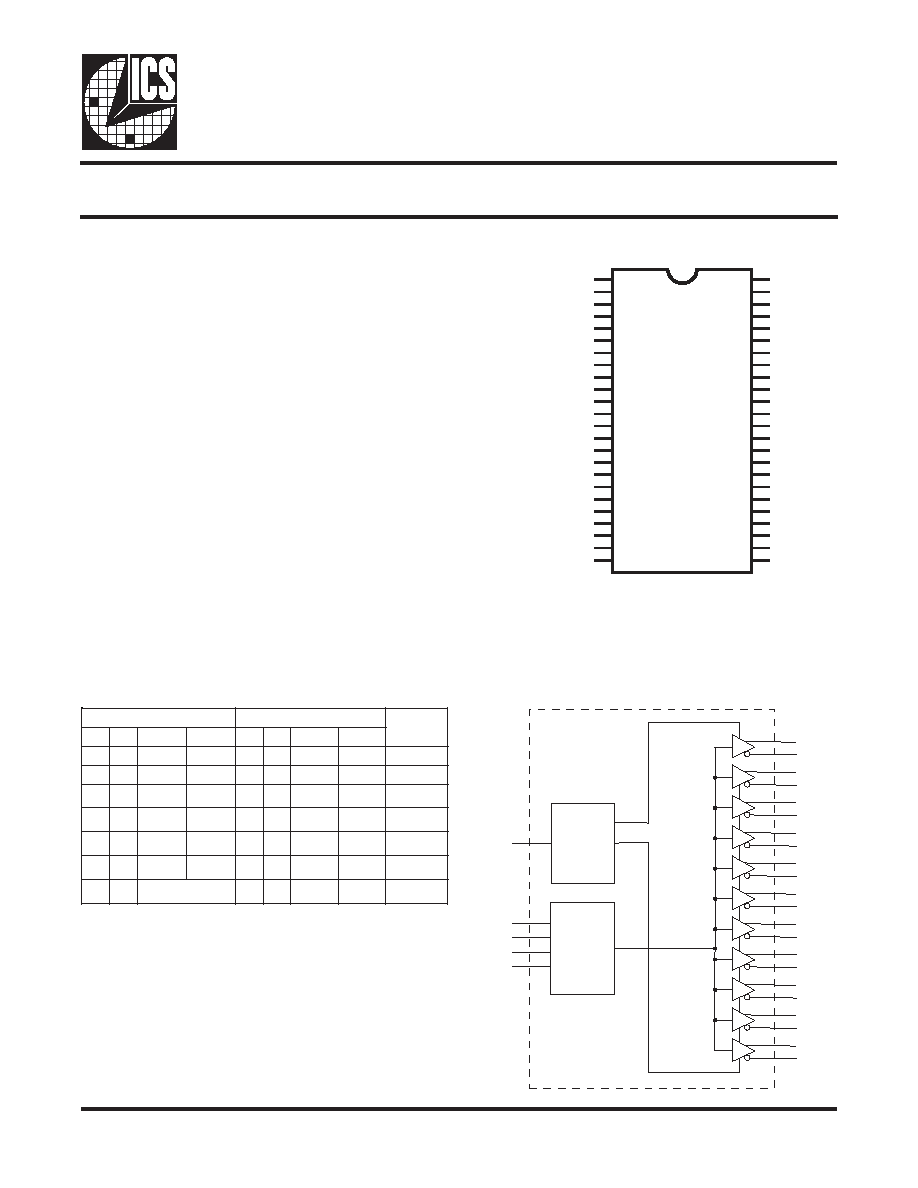
Block Diagram
Value SSTL_2 Clock Driver (60MHz - 220MHz)
Pin Configuration
48-Pin TSSOP
Recommended Application:
Zero delay board fan-out memory modules
Product Description/Features:
·
Meets PC3200 specification for DDRI-400 support
·
Low skew, low jitter PLL clock driver
·
1 to 10 differential clock distribution (SSTL_2)
·
Feedback pins for input to output synchronization
·
PD# for power management
·
Spread Spectrum tolerant inputs
·
Auto PD when input signal removed
Switching Characteristics:
·
CYCLE - CYCLE jitter (>100MHz):<75ps
·
OUTPUT - OUTPUT skew: <100ps
S
T
U
P
N
I
S
T
U
P
T
U
O
e
t
a
t
S
L
L
P
D
D
V
A
#
D
P
T
N
I
_
K
L
C
C
N
I
_
K
L
C
T
K
L
C
C
K
L
C
T
T
U
O
_
B
F
C
T
U
O
_
B
F
D
N
G
H
L
H
L
H
L
H
f
f
o
/
d
e
s
s
a
p
y
B
D
N
G
H
H
L
H
L
H
L
f
f
o
/
d
e
s
s
a
p
y
B
V
5
.
2
)
m
o
n
(
L
L
H
Z
Z
Z
Z
f
f
o
V
5
.
2
)
m
o
n
(
L
H
L
Z
Z
Z
Z
f
f
o
V
5
.
2
)
m
o
n
(
H
L
H
L
H
L
H
n
o
V
5
.
2
)
m
o
n
(
H
H
L
H
L
H
L
n
o
V
5
.
2
)
m
o
n
(
X
)
z
H
M
0
2
<
)
1
(
Z
Z
Z
Z
f
f
o
Functionality
PLL
FB_INT
FB_INC
CLK_INC
CLK_INT
PD#
Control
Logic
FB_OUTT
FB_OUTC
CLKT0
CLKT1
CLKT2
CLKT3
CLKT4
CLKT5
CLKT6
CLKT7
CLKT8
CLKT9
CLKC0
CLKC1
CLKC2
CLKC3
CLKC4
CLKC5
CLKC6
CLKC7
CLKC8
CLKC9
6.10 mm. Body, 0.50 mm. pitch TSSOP
GND
CLKC0
CLKT0
VDD
CLKT1
CLKC1
GND
GND
CLKC2
CLKT2
VDD
VDD
CLK_INT
CLK_INC
VDD
AVDD
AGND
GND
CLKC3
CLKT3
VDD
CLKT4
CLKC4
GND
GND
CLKC5
CLKT5
VDD
CLKT6
CLKC6
GND
GND
CLKC7
CLKT7
VDD
PD#
FB_INT
FB_INC
VDD
FB_OUTC
FB_OUTT
GND
CLKC8
CLKT8
VDD
CLKT9
CLKC9
GND
ICS91
8
57
1
2
3
4
5
6
7
8
9
10
11
12
13
14
15
16
17
18
19
20
21
22
23
24
48
47
46
45
44
43
42
41
40
39
38
37
36
35
34
33
32
31
30
29
28
27
26
25
2
ICS91857
0494C--08/15/05
Pin Descriptions
R
E
B
M
U
N
N
I
P
E
M
A
N
N
I
P
E
P
Y
T
N
O
I
T
P
I
R
C
S
E
D
,
1
2
,
5
1
,
2
1
,
1
1
,
4
,
5
4
,
8
3
,
4
3
,
8
2
D
D
V
R
W
P
.
3
3
3
R
D
D
o
t
p
u
V
5
.
2
y
l
p
p
u
s
r
e
w
o
P
.
z
H
M
0
0
4
t
a
I
-
R
D
D
r
o
f
V
6
.
2
y
l
p
p
u
s
r
e
w
o
P
,
5
2
,
4
2
,
8
1
,
8
,
7
,
1
8
4
,
2
4
,
1
4
,
1
3
D
N
G
R
W
P
d
n
u
o
r
G
6
1
D
D
V
A
R
W
P
.
3
3
3
R
D
D
o
t
p
u
V
5
.
2
,
y
l
p
p
u
s
r
e
w
o
p
g
o
l
a
n
A
.
z
H
M
0
0
4
t
a
I
-
R
D
D
r
o
f
V
6
.
2
y
l
p
p
u
s
r
e
w
o
P
7
1
D
N
G
A
R
W
P
.
d
n
u
o
r
g
g
o
l
a
n
A
,
6
4
,
4
4
,
9
3
,
9
2
,
7
2
3
,
5
,
0
1
,
0
2
,
2
2
)
0
:
9
(
T
K
L
C
T
U
O
.
s
t
u
p
t
u
o
r
i
a
p
l
a
i
t
n
e
r
e
f
f
i
d
f
o
k
c
o
l
C
"
e
u
r
T
"
,
7
4
,
3
4
,
0
4
,
0
3
,
6
2
2
,
6
,
9
,
9
1
,
3
2
)
0
:
9
(
C
K
L
C
T
U
O
.
s
t
u
p
t
u
o
r
i
a
p
l
a
i
t
n
e
r
e
f
f
i
d
f
o
s
k
c
o
l
c
"
y
r
a
t
n
e
m
e
l
p
m
o
C
"
4
1
C
N
I
_
K
L
C
N
I
t
u
p
n
i
k
c
o
l
c
e
c
n
e
r
e
f
e
r
"
y
r
a
t
n
e
m
e
l
p
m
o
C
"
3
1
T
N
I
_
K
L
C
N
I
t
u
p
n
i
k
c
o
l
c
e
c
n
e
r
e
f
e
r
"
e
u
r
T
"
3
3
C
T
U
O
_
B
F
T
U
O
t
I
.
k
c
a
b
d
e
e
f
l
a
n
r
e
t
x
e
r
o
f
d
e
t
a
c
i
d
e
d
,
t
u
p
t
u
o
k
c
a
b
d
e
e
F
"
y
r
a
t
n
e
m
e
l
p
m
o
C
"
d
e
r
i
w
e
b
t
s
u
m
t
u
p
t
u
o
s
i
h
T
.
K
L
C
e
h
t
s
a
y
c
n
e
u
q
e
r
f
e
m
a
s
e
h
t
t
a
s
e
h
c
t
i
w
s
.
C
N
I
_
B
F
o
t
2
3
T
T
U
O
_
B
F
T
U
O
t
a
s
e
h
c
t
i
w
s
t
I
.
k
c
a
b
d
e
e
f
l
a
n
r
e
t
x
e
r
o
f
d
e
t
a
c
i
d
e
d
,
t
u
p
t
u
o
k
c
a
b
d
e
e
F
"
e
u
r
T
"
.
T
N
I
_
B
F
o
t
d
e
r
i
w
e
b
t
s
u
m
t
u
p
t
u
o
s
i
h
T
.
K
L
C
e
h
t
s
a
y
c
n
e
u
q
e
r
f
e
m
a
s
e
h
t
6
3
T
N
I
_
B
F
N
I
r
o
f
L
L
P
l
a
n
r
e
t
n
i
e
h
t
o
t
l
a
n
g
i
s
k
c
a
b
d
e
e
f
s
e
d
i
v
o
r
p
,
t
u
p
n
i
k
c
a
b
d
e
e
F
"
e
u
r
T
"
.
r
o
r
r
e
e
s
a
h
p
e
t
a
n
i
m
il
e
o
t
T
N
I
_
K
L
C
h
t
i
w
n
o
i
t
a
z
i
n
o
r
h
c
n
y
s
5
3
C
N
I
_
B
F
N
I
L
L
P
l
a
n
r
e
t
n
i
e
h
t
o
t
l
a
n
g
i
s
s
e
d
i
v
o
r
p
,
t
u
p
n
i
k
c
a
b
d
e
e
F
"
y
r
a
t
n
e
m
e
l
p
m
o
C
"
.
r
o
r
r
e
e
s
a
h
p
e
t
a
n
i
m
il
e
o
t
C
N
I
_
K
L
C
h
t
i
w
n
o
i
t
a
z
i
n
o
r
h
c
n
y
s
r
o
f
7
3
#
D
P
N
I
t
u
p
n
i
S
O
M
C
V
L
.
n
w
o
D
r
e
w
o
P
This PLL Clock Buffer is designed for a V
DD
of 2.5V, an AV
DD
of 2.5V and differential data input and output levels.
ICS91857 is a zero delay buffer that distributes a differential clock input pair (CLK_INC, CLK_INT) to ten differential
pair of clock outputs (CLKT[0:9], CLKC[0:9]) and one differential pair feedback clock output (FB_OUT, FB_OUTC). The
clock outputs are controlled by the input clocks (CLK_INC, CLK_INT), the feedback clocks (FB_INT, FB_INC) the 2.5-
V LVCMOS input (PD#) and the Analog Power input (AV
DD
). When input (PD#) is low while power is applied, the receivers
are disabled, the PLL is turned off and the differential clock outputs are Tri-Stated. When AV
DD
is grounded, the PLL
is turned off and bypassed for test purposes.
When the input frequency is less than the operating frequency of the PLL, appproximately 20MHz, the device will
enter a low power mode. An input frequency detection circuit on the differential inputs, independent from the input
buffers, will detect the low frequency condition and perform the same low power features as when the (PD#) input
is low. When the input frequency increases to greater than approximately 20 MHz, the PLL will be turned back on,
the inputs and outputs will be enabled and PLL will obtain phase lock between the feedback clock pair (FB_INT,
FB_INC) and the input clock pair (CLK_INC, CLK_INT).
The PLL in the ICS91857 clock driver uses the input clocks (CLK_INC, CLK_INT) and the feedback clocks (FB_INT,
FB_INC) provide high-performance, low-skew, low-jitter output differential clocks (CLKT [0:9], CLKC [0:9]). The
ICS91857 is also able to track Spread Spectrum Clock (SSC) for reduced EMI.
ICS91857 is characterized for operation from 0°C to 70°C and will meet JEDEC Standard 82-1 and 82-1A for Registered
DDR Clock Driver.
3
ICS91857
0494C--08/15/05
Absolute Maximum Ratings
Supply Voltage (VDD & AVDD) . . . . . . . . . . -0.5V to 4.6V
Logic Inputs . . . . . . . . . . . . . . . . . . . . . . . . . GND 0.5 V to V
DD
+ 0.5 V
Ambient Operating Temperature . . . . . . . . . 0°C to +70°C
Storage Temperature . . . . . . . . . . . . . . . . . . 65°C to +150°C
Stresses above those listed under
Absolute Maximum Ratings may cause permanent damage to the device. These
ratings are stress specifications only and functional operation of the device at these or any other conditions above
those listed in the operational sections of the specifications is not implied. Exposure to absolute maximum rating
conditions for extended periods may affect product reliability.
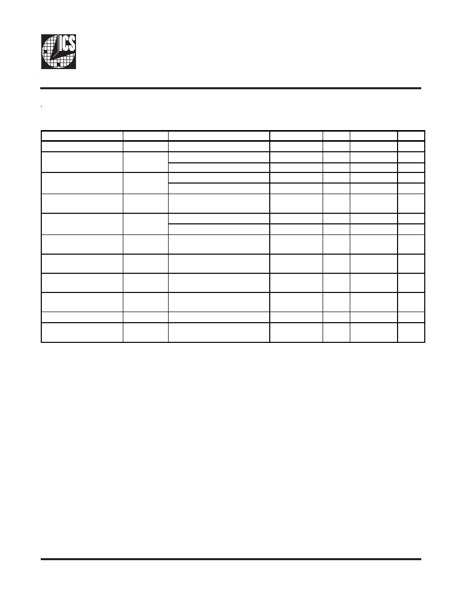
Electrical Characteristics for DDR200/266/333 - Input/Supply/Common Output Parameters
T
A
= 0 - 70°C; Supply Voltage A
VDD
, V
DD
= 2.5V ± 0.2V (unless otherwise stated)
PARAMETER
SYMBOL
CONDITIONS
MIN
TYP
MAX
UNITS
Input High Current
I
IH
V
I
= V
DD
or GND
5
µA
Input Low Current
I
IL
V
I
= V
DD
or GND
5
µA
I
DD2.5
C
L
= 0pf @ 200MHz
260
mA
I
DDPD
C
L
= 0pf
100
mA
Output High Current
I
OH
V
DD
= 2.3V, V
OUT
= 1V
-18
-32
mA
Output Low Current
I
OL
V
DD
= 2.3V, V
OUT
= 1.2V
26
35
mA
High Impedance
Output Current
I
OZ
V
DD
=2.7V, Vout=V
DD
or GND
±10
mA
Input Clamp Voltage
V
IK
V
DDQ
= 2.3V Iin = -18mA
-1.2
V
V
DD
= min to max,
I
OH
= -1 mA
V
DDQ
- 0.1
V
V
DDQ
= 2.3V,
I
OH
= -12 mA
1.7
V
V
DD
= min to max
I
OL
=1 mA
0.1
V
V
DDQ
= 2.3V
I
OH
=12 mA
0.6
V
Input Capacitance
1
C
IN
V
I
= GND or V
DD
3
pF
Output Capacitance
1
C
OUT
V
OUT
= GND or V
DD
3
pF
1
Guaranteed by design at 170MHz, not 100% tested in production.
Operating Supply
Current
High-level output
voltage
V
OH
Low-level output voltage
V
OL
4
ICS91857
0494C--08/15/05
Electrical Characteristics for DDRI-400 - Input/Supply/Common Output Parameters
T
A
= 0 - 70°C; Supply Voltage A
VDD
, V
DD
= 2.6V ± 0.1V
PARAMETER
SYMBOL
CONDITIONS
MIN
TYP
MAX
UNITS
Input High Current
I
IH
V
I
= V
DD
or GND
5
µA
Input Low Current
I
IL
V
I
= V
DD
or GND
5
µA
I
DD2.5
C
L
= 0pf @ 200MHz
260
mA
I
DDPD
C
L
= 0pf
100
mA
Output High Current
I
OH
V
DD
= 2.3V, V
OUT
= 1V
-18
-32
mA
Output Low Current
I
OL
V
DD
= 2.3V, V
OUT
= 1.2V
26
35
mA
High Impedance
Output Current
I
OZ
V
DD
=2.7V, Vout=V
DD
or GND
±10
mA
Input Clamp Voltage
V
IK
V
DDQ
= 2.3V Iin = -18mA
-1.2
V
V
DD
= min to max,
I
OH
= -1 mA
V
DDQ
- 0.1
V
V
DDQ
= 2.3V,
I
OH
= -12 mA
1.7
V
V
DD
= min to max
I
OL
=1 mA
0.1
V
V
DDQ
= 2.3V
I
OH
=12 mA
0.6
V
Input Capacitance
1
C
IN
V
I
= GND or V
DD
3
pF
Output Capacitance
1
C
OUT
V
OUT
= GND or V
DD
3
pF
1
Guaranteed by design at 220MHz, not 100% tested in production.
Operating Supply
Current
High-level output
voltage
V
OH
Low-level output voltage
V
OL
5
ICS91857
0494C--08/15/05
Recommended Operating Condition for DDR200/266/333 (see note1)
T
A
= 0 - 85°C; Supply Voltage AVDD, VDD = 2.5V ± 0.2V (unless otherwise stated)
PARAMETER
SYMBOL
CONDITIONS
MIN
TYP
MAX
UNITS
Supply Voltage
V
DDQ
, A
VDD
2.3
2.7
V
CLKT, CLKC, FB_INC
V
DDQ
/2 - 0.18
V
PD#
-0.3
0.7
V
CLKT, CLKC, FB_INC
V
DDQ
/2 + 0.18
V
PD#
1.7
V
DDQ
+ 0.6
V
DC input signal voltage
(note 2)
-0.3
V
DDQ
V
DC - CLKT, FB_INT
0.36
V
DDQ
+ 0.6
V
AC - CLKT, FB_INT
0.7
V
DDQ
+ 0.6
V
Output differential cross-
voltage (note 4)
V
OX
V
DDQ
/2 - 0.15
V
DDQ
/2 + 0.15
V
Input differential cross-
voltage (note 4)
V
IX
V
DDQ
/2 - 0.2
V
DDQ
/2 + 0.2
V
High level output
current
I
OH
0.12
mA
Low level output current
I
OL
12
mA
Input slew rate
S
R
1
4
V/ns
Operating free-air
temperature
T
A
0
70
°C
Differential input signal
voltage (note 3)
V
ID
Low level input voltage
V
IL
High level input voltage
V
IH
Notes:
1.
Unused inputs must be held high or low to prevent them from floating.
2.
DC input signal voltage specifies the allowable DC execution of differential input.
3.
Differential inputs signal voltages specifies the differential voltage [VTR-VCP]
required for switching, where VT is the true input level and VCP is the
complementary input level.
4.
Differential cross-point voltage is expected to track variations of V
CC
and is the
voltage at which the differential signal must be crossing.