Integrated
Circuit
Systems, Inc.
General Description
Features
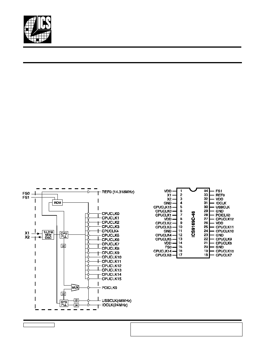
ICS9169C-46
Block Diagram
Frequency Generator for PentiumPro Based Systems
9169C-46RevA072597P
Pin Configuration
34-Pin SSOP
Pentium is a trademark on Intel Corporation.
16 selectable CPU clocks up to 66.66 MHz
One synchronous PCI clock.
One USB clock at 48MHz, meets Intel jitter,
accuracy, as well as rise and fall time requirements
One I/O clock at 24MHz
One Ref. Clock at 14.318MHz
CPU clocks to PCI clock skew of 1-4ns (CPU early)
Low CPU and PCI clock jitter <200ps
Low skew outputs, skew window 250ps for CPU
clocks and for PCI clocks
Improved output drivers are designed for low EMI
Test Mode
3.3V �10% operation
Space saving and low cost 34-pin SSOP package
The ICS9169C-46 is a Clock Synthesize/Driver chip for
Pentium, PentiumPro or Cyrix 68x86 based motherboards
using SDRAM.
Features include sixteen CPU outputs, twelve of which can
be used to support up to three SDRAM modules. The
PCICLK output can be buffered with an external, low cost
zero delay buffer. Additionally, the device meets the
Pentium and PentiumPro power-up stabilization, which
requires that CPU and PCI clocks be stable within 2ms after
power-up.
The ICS9169C-46 clock outputs are designed for low EMI
emissions. Controlled rise and fall times, unique output
driver circuits and innovative circuit layout techniques enable
the ICS9169C-46 to have lower EMI than other clock
devices.
The ICS9169C-46 accepts a 14.318MHz reference crystal
or clock as its input and runs from a 3.3V supply.
ICS reserves the right to make changes in the device data identified in this
publication without further notice. ICS advises its customers to obtain the latest
version of all device data to verify that any information being relied upon by the
customer is current and accurate.
2
ICS9169C-46
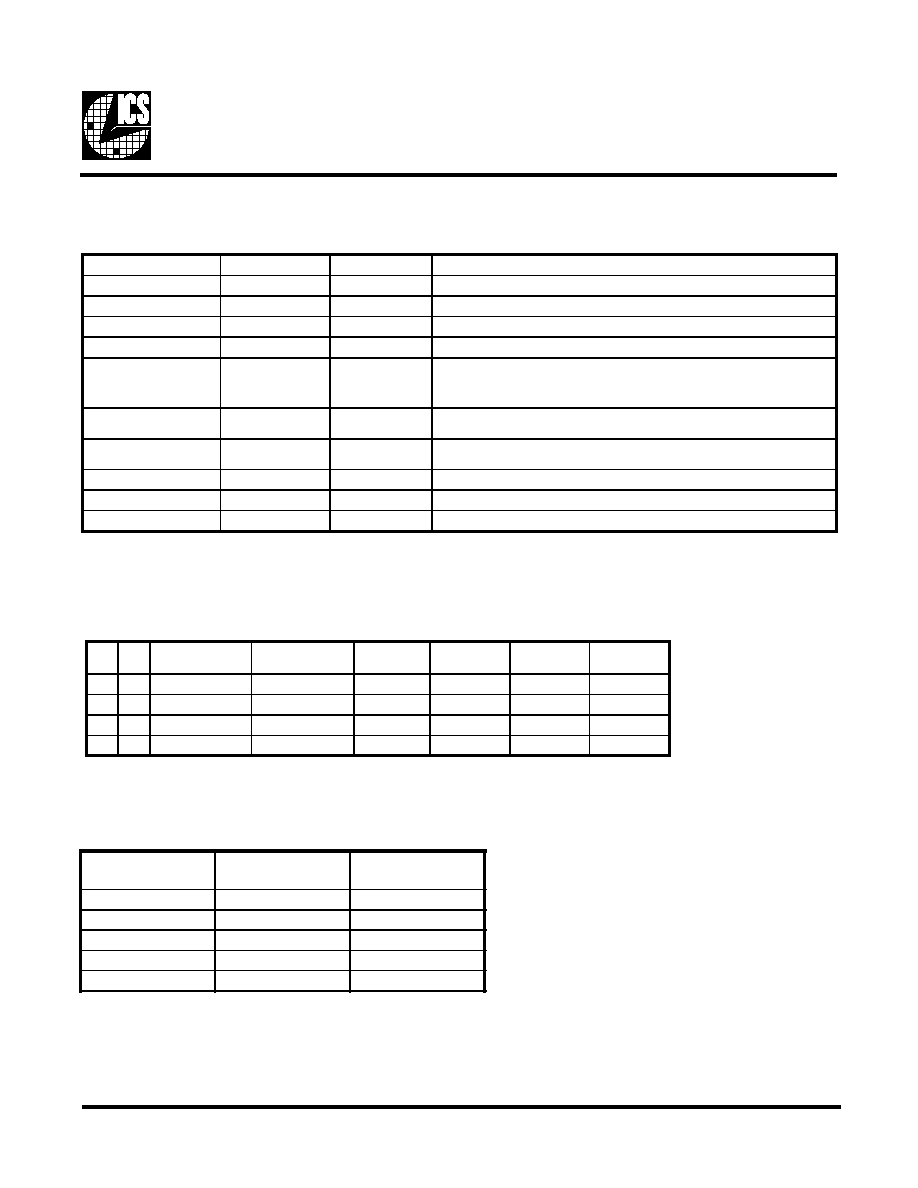
Pin Descriptions
Functionality
3.3V�10%, 0-70
�
C
Crystal (X1, X2) = 14.31818 MHz
FS1
FS0
XTALIN
CPUCLK (0:15)
(MHz)
PCICLK0
(MHz)
REF(0:1)
(MHz)
USBCLK
(MHz)
IOCLK
(MHz)
0
0
14.318MHz
Hi-Z
Hi-Z
Hi-Z
Hi-Z
Hi-Z
0
1
14.318MHz
66.67
33.3
14.318
48
24
1
0
14.318MHz
50.0
25.0
14.318
48
24
1
1
14.318MHz
60.0
30.0
14.318
48
24
Actual Output Frequencies
Output Clocks
Target Frequency
(MHz)
Actual Frequency
(MHz)
CPUCLK (0:15)
50.0
48.83
CPUCLK (0:15)
60.0
60.0
CPUCLK (0:15)
66.67
68.66
USBCLK
48
48.008
IOCLK
24
24.004
PIN NUMBER
PIN NAME
TYPE
DESCRIPTION
1, 8, 14, 26, 32
V
D D
PWR
Voltage Supply
2
X1
IN
Reference crystal input
3
X2
OUT
Reference crystal feedback
4, 11 20, 23, 29
GND
PWR
Ground
5, 6, 7, 9, 10, 12,
13, 16, 17, 18, 19,
21, 22, 24, 25, 27
CPUCLK(0:15)
OUT
CPU clock outputs
15, 34
FS (0:1)
IN
CPU clock select input bits. These devices have internal pull-ups
28
PCICLK
OUT
BUS clock output
30
USBCLK
OUT
USB clock output 48 MHz
31
IOCLK
OUT
I/O clock output 24 MHz
33
REF0
OUT
Reference clock output (14.318 MHz)

3
ICS9169C-46
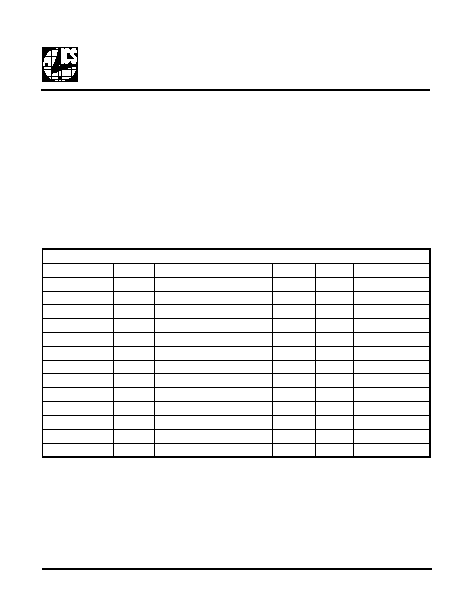
Technical Pin Function Descriptions
VDD
This is the power supply to the internal logic of the device as
well as the following clock output buffers:
This pin may be operated at any voltage between 3.0 to 3.7
volts. Clocks from the listed buffers that it supplies will have
a voltage swing from ground to this level. For the actual
guaranteed high and low voltage levels of these clocks,
please consult the AC parameter table in this data sheet.
GND (VSS)
This is the power supply ground return pin for the internal
logic of the device as well as the following clock output
buffers:
A. REF clock output buffers
B. CPU clock output buffers
X1
This pin serves one of two functions. When the device is
used with a crystal, X1 acts as the input pin for the
reference signal that comes from the discrete crystal.
When the device is driven by an external clock signal, X1
is the device input pin for that reference clock. This pin
also implements an internal crystal loading capacitor that
is connected to ground. See the data tables for the value of
the capacitor.
X2
This pin is used only when the device uses a Crystal as the
reference frequency source. In this mode of operation, X2
is an output signal that drives (or excites) the discrete
crystal. This pin also implements an internal crystal loading
capacitor that is connected to ground. See the data tables
for the value of the capacitor.
CPUCLK (0:15)
This pin is the clock output that drives processor and other
CPU related circuitry that require clocks which are in tight
skew tolerance with the CPU clock. See the Functionality
table at the beginning of this data sheet for a list of the
specific frequencies that this clock operates at and the
selection codes that are necessary to produce these
frequencies.
PCICLK
Clock output driver.
FS0, FS1
These pins control the frequency of the clocks at the CPU,
and PCI. See the Funtionality table at the beginning of this
data sheet for a list of the specific frequencies that this clock
operates at and the selection codes that are necessary to
produce these frequencies. If a "1" value is desired for a
specific frequency selection bit,a 10K ohm restor must be
connected from the appropriate FS pin to the VDD supply. If
a "0" value is desired, then the 10K resistor must be connected
to ground.
48MHz
This is a fixed frequency clock that is typicaly used to drive
USB peripheral device needs.
24MHz
This is a fixed frequency clock that is typicaly used to drive
super I/O peripheral device needs.
REF0
This is a fixed frequency clock that runs at the same frequency
as the input freerence clock (typically 14.31818 MHz) is
and typically used to drive Video and ISA BUS requirements.
4
ICS9169C-46
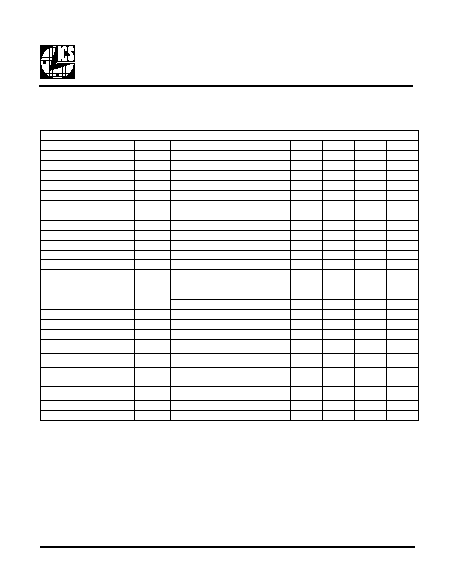
Absolute Maximum Ratings
Electrical Characteristics at 3.3V
Supply Voltage . . . . . . . . . . . . . . . . . . . . . . . . . . . 7.0 V
Logic Inputs . . . . . . . . . . . . . . . . . . . . . . . . . . . . GND 0.5 V to V
DD
+0.5 V
Ambient Operating Temperature . . . . . . . . . . . . 0�C to +70�C
Storage Temperature . . . . . . . . . . . . . . . . . . . . . . 65�C to +150�C
V
DD
= 3.0 3.7 V, T
A
= 0 70
�
C unless otherwise stated
Note 1: Parameter is guaranteed by design and characterization. Not 100% tested in production.
Stresses above those listed under Absolute Maximum Ratings may cause permanent damage to the device. These ratings are
stress specifications only and functional operation of the device at these or any other conditions above those listed in the
operational sections of the specifications is not implied. Exposure to absolute maximum rating conditions for extended periods
may affect product reliability.
DC Characteristics
PARAMETER
SYMBOL
TEST CONDITIONS
MIN
TYP
MAX
UNITS
Input Low Voltage
V
IL
-
-
0.2V
D D
V
Input High Voltage
V
IH
0.7V
D D
-
-
V
Input Low Current
I
IL
VIN=0V
-28.0
-10.5
-
�A
Input High Current
I
IH
VIN=V
D D
-5.0
-
5.0
�A
Output Low Current
1
I
O L
VOL=0.8V; for CPU, PCI, REF CLKS
16.0
25.0
-
mA
Output High Current
1
I
O H
VOL=2.0V; for CPU, PCI, REF CLKS
-
-30.0
-14.0
mA
Output Low Current
1
I
O L
VOL=0.8V; for Fixed CLK
19.0
30.0
-
mA
Output High Current
1
I
O H
VOL=2.0V; for Fixed CLK
-
-38.0
-16.0
mA
Output Low Voltage
1
V
O L
IOL=8mA; for CPU, PCI, REF
-
0.3
0.4
V
Output High Voltage
1
V
O H
IOH=-8mA; for CPU, PCI, REF
2.4
2.8
-
V
Output Low Voltage
1
V
O L
IOL=18mA; Fixed CLK's
-
0.3
0.4
V
Output High Voltage
1
V
O H
IOH=-18mA; Fixed CLK's
2.4
2.8
-
V
Supply Current
I
D D
@66.6 MHz; all outputs unloaded
-
95
115
mA
5
ICS9169C-46
Electrical Characteristics at 3.3V
V
DD
= 3.0 3.7 V, T
A
= 0 70
�
C unless otherwise stated
Note 1: Parameter is guaranteed by design and characterization. Not 100% tested in production.
AC Characteristics
PARAMETER
SYMBOL
TEST CONDITIONS
MIN
TYP
MAX
UNITS
Rise Time
1
T
r1
20pF load, 0.8 to 2.0V; All Except Ref
-
0.9
1.2
ns
Fall Time
1
T
f1
20pF load, 2.0 to 0.8V; All Except Ref
-
0.8
1.2
ns
Rise Time
1
T
r2
30pF load, 0.8 - 2.0V All Except Ref
-
1.1
1.4
ns
Fall Time
1
T
f2
30pF load, 2.0 - 0.8V All Except Ref
-
1.0
1.2
ns
Rise Time
1
T
r3
45pF load; 0.8 - 2.0V; Ref
1.6
2.4
ns
Fall Time
1
T
f3
45pF load; 2.0 - 0.8V; Ref
1.4
2.4
ns
Duty Cycle
1
D
t
20, 30, 45pF load @ VOUT=1.5V
45
50
55
%
Jitter, One Sigma
1
T
j1s1
CPU & PCI Clocks
-
50
150
ps
Jitter, Absolute
1
T
jab1
CPU & PCI Clocks (@ 60 & 66MHz)
-250
-
250
ps
Jitter, Absolute
1
T
jab1
CPU & PCI Clocks (50MHz)
-400
-
400
ps
Jitter, One Sigma
1
T
j1s2
Ref & Fixed CLKs
-
1
3
%
Jitter, Absolute
1
T
jab2
Ref & Fixed CLKs
-25
1.0
2.5
%
Jitter - Cycle to Cycle
T
cc
CPU Outputs
-
290
350
ps
PCI Output
-
350
500
ps
REF0
-
1.5
2.0
%
Fixed Clocks
-
4.5
6
%
Input Frequency
1
F
i
12.0
14.318
16.0
MHz
Logic Input Capacitance
1
C
IN
Logic input pins
-
5
-
pF
Crystal Oscillator Capacitance
1
C
INX
X1, X2 pins
-
18
-
pF
Power-on Time
1
t
on
From V
DD
=1.6V to 1st crossing of 66.6
MHz V
DD
supply ramp < 40ms
-
1.9
2.0
ms
Frequency Settling Time
1
t
s
From 1st crossing of acquisition to
<1% settling
-
2.0
4.0
ms
Clock Skew
1
(window)
T
sk1
CPU to CPU; Same Load; @1.5V
-
188
250
ps
Clock Skew
1
(window)
T
sk2
CPU(20pF) - CPU (30pF); @1.5V
-
300
500
ps
Clock Skew
1
T
sk3
CPU 20pF to PCI 7.5pF, @ 1.5V
(CPU is Early)
1
1.2
3.0
ns
Rise Time
T
r3
45pF; 0.8 - 2.0V; Ref only
-
1.6
2.4
ns
Fall Time
T
f3
45pF; 2.0 - 0.8V; Ref only
-
1.4
2.4
ns