Äîêóìåíòàöèÿ è îïèñàíèÿ www.docs.chipfind.ru
Integrated Circuit Solution, Inc.
1
SR027-0C
ICSI reserves the right to make changes to its products at any time without notice in order to improve design and supply the best possible product. We assume no responsibility for any errors
which may appear in this publication. © Copyright 2000, Integrated Circuit Solution, Inc.
FEATURES
High-speed access times:
8, 10, 12 and 15 ns
High-preformance, lower-power CMOS process
Multiple center power and ground pins for
greater noise immunity
Easy memory expansion with CE and OE
options
CE power-down
Fully static operation: no clock or refresh
reguired
TTL compatible inputs and outputs
Single 3.3V + 10% power supply
Packages available:
36-pin 400mil SOJ
44-pin TSOP-2
DESCRIPTION
The
1+51
IS61LV5128 is a very high-speed, low power,
524,288-word by 8-bit COMS static RAM. The IS61LV5128 is
fabricated using
1+51
's high-performance CMOS technology.
This highly reliable process coupled with innovative circuit
design techniques, yields higher preformance and low power
consumotion devices.
When CE is HIGH (deselected), the device assumes a standby
mode at which the power dissipation can be reduced down to
250 µW (typical) with CMOS input levels.
The IS61LV5128 operates from a single 3.3V power supply
and all inputs are TTL-compatible.
The IS61LV5128 is available in 36-pin, 400mil SOJ and 44-pin
TSOP-2 package.
IS61LV5128
512K x 8 HIGH-SPEED CMOS STATIC RAM
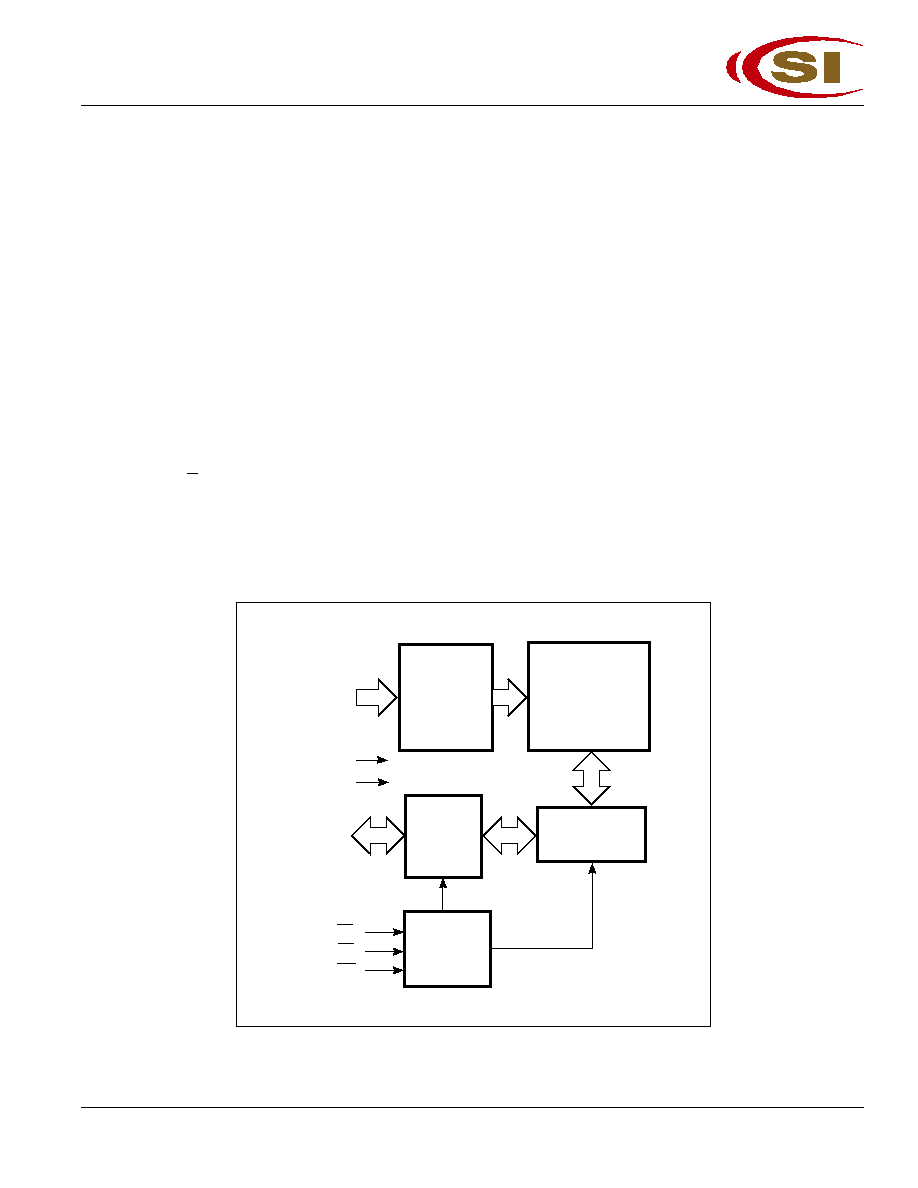
FUNCTIONAL BLOCK DIAGRAM
A0-A18
CE
OE
WE
512K X 8
MEMORY ARRAY
DECODER
COLUMN I/O
CONTROL
CIRCUIT
GND
VCC
I/O
DATA
CIRCUIT
I/O0-I/O7
IS61LV5128
2
Integrated Circuit Solution, Inc.
SR027-0C
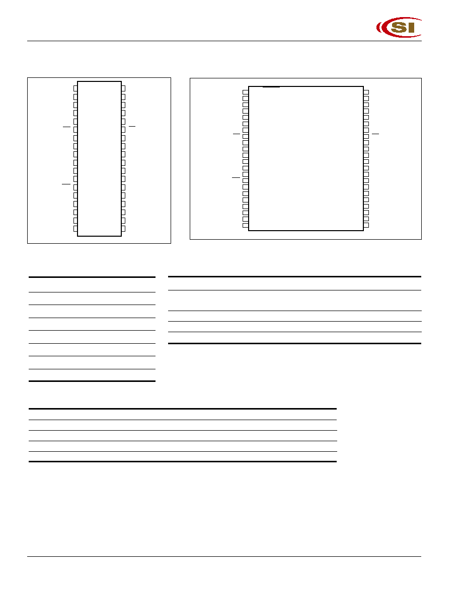
PIN CONFIGURATION
36-Pin SOJ
1
2
3
4
5
6
7
8
9
10
11
12
13
14
15
16
17
18
19
20
21
22
44
43
42
41
40
39
38
37
36
35
34
33
32
31
30
29
28
27
26
25
24
23
NC
NC
A0
A1
A2
A3
A4
CE
I/O0
I/O1
Vcc
GND
I/O2
I/O3
WE
A5
A6
A7
A8
A9
NC
NC
NC
NC
NC
A18
A17
A16
A15
OE
I/O7
I/O6
GND
Vcc
I/O5
I/O4
A14
A13
A12
A11
A10
NC
NC
NC
1
2
3
4
5
6
7
8
9
10
11
12
13
14
15
16
17
18
36
35
34
33
32
31
30
29
28
27
26
25
24
23
22
21
20
19
A0
A1
A2
A3
A4
CE
I/O0
I/O1
Vcc
GND
I/O2
I/O3
WE
A5
A6
A7
A8
A9
NC
A18
A17
A16
A15
OE
I/O7
I/O6
GND
Vcc
I/O5
I/O4
A14
A13
A12
A11
A10
NC
PIN CONFIGURATION
44-Pin TSOP-2
PIN DESCRIPTIONS
A0-A18
Address Inputs
CE
Chip Enable Input
OE
Output Enable Input
WE
Write Enable Input
I/O0-I/O7
Input/Output
Vcc
Power
GND
Ground
NC
No Connection
TRUTH TABLE
Mode
WE
WE
WE
WE
WE
CE
CE
CE
CE
CE
OE
OE
OE
OE
OE
I/O Operation
Vcc Current
Not Selected
X
H
X
High-Z
I
SB
, I
SB
(Power-down)
Output Disabled
H
L
H
High-Z
I
CC
Read
H
L
L
D
OUT
I
CC
Write
L
L
X
D
IN
I
CC
ABSOLUTE MAXIMUM RATINGS
(1)
Symbol
Parameter
Value
Unit
V
TERM
Terminal Voltage with Respect to GND
0.5 to Vcc + 0.5 V
T
BIAS
Temperature Under Bias
55 to +125
°C
T
STG
Storage Temperature
65 to +150
°C
P
D
Power Dissipation
1.0
W
Notes:
1. Stress greater than those listed under ABSOLUTE MAXIMUM RATINGS may cause permanent
damage to the device. This is a stress rating only and functional operation of the device at these or any
other conditions above those indicated in the operational sections of this specification is not implied.
Exposure to absolute maximum rating conditions for extended periods may affect reliability.
IS61LV5128
Integrated Circuit Solution, Inc.
3
SR027-0C
DC ELECTRICAL CHARACTERISTICS
(Over Operating Range)
Symbol Parameter
Test Conditions
Min.
Max.
Unit
V
OH
Output HIGH Voltage
V
CC
= Min., I
OH
= 4.0 mA
2.4
V
V
OL
Output LOW Voltage
V
CC
= Min., I
OL
= 8.0 mA
0.4
V
V
IH
Input HIGH Voltage
2.0
V
CC
+ 0.3
V
V
IL
Input LOW Voltage
0.3
0.8
V
I
LI
Input Leakage
GND V
IN
V
CC
Com.
1
1
µA
Ind.
5
5
I
LO
Output Leakage
GND V
OUT
V
CC
, Outputs Disabled
Com.
1
1
µA
Ind.
5
5
Notes:
1. V
IL
= 3.0V for pulse width less than 10 ns.
2. The Vcc operating range for 8 ns is 3.3V +10%, -5%.
CAPACITANCE
(1,2)
Symbol
Parameter
Conditions
Max.
Unit
C
IN
Input Capacitance
V
IN
= 0V
6
pF
C
OUT
Output Capacitance
V
OUT
= 0V
8
pF
Notes:
1. Tested initially and after any design or process changes that may affect these parameters.
2. Test conditions: T
A
= 25°C, f = 1 MHz, Vcc = 3.3V.
OPERATING RANGE
Range
Ambient Temperature
V
CC
Commercial
0°C to +70°C
3.3V + 10%
Industrial
40°C to +85°C
3.3V + 10%
POWER SUPPLY CHARACTERISTICS
(1)
(Over Operating Range)
-8 ns
-10 ns
-12 ns
-15 ns
Symbol Parameter
Test Conditions
Min. Max.
Min. Max.
Min. Max.
Min. Max. Unit
I
CC
Vcc Dynamic Operating
V
CC
= Max.,
Com.
300
280
260
240
mA
Supply Current
I
OUT
= 0 mA, f = f
MAX
Ind.
310
290
270
250
I
SB
TTL Standby Current
V
CC
= Max.,
Com.
55
55
55
55
mA
(TTL Inputs)
V
IN
= V
IH
or V
IL
Ind.
65
65
65
65
CE V
IH
, f = 0
I
SB
CMOS Standby
V
CC
= Max.,
Com.
10
10
10
10
mA
Current (CMOS Inputs)
CE V
CC
0.2V,
Ind.
15
15
15
15
V
IN
V
CC
0.2V, or
V
IN
0.2V, f = 0
Note:
1. At f = f
MAX
, address and data inputs are cycling at the maximum frequency, f = 0 means no input lines change.
IS61LV5128
4
Integrated Circuit Solution, Inc.
SR027-0C
AC TEST CONDITIONS
Parameter
Unit
Input Pulse Level
0V to 3.0V
Input Rise and Fall Times
3 ns
Input and Output Timing
1.5V
and Reference Levels
Output Load
See Figures 1 and 2
Notes:
1. The Vcc operating range for 8 ns is 3.3V +10%, -5%.
READ CYCLE SWITCHING CHARACTERISTICS
(1)
(Over Operating Range)
-8
-10
-12
-15
Symbol Parameter
Min. Max.
Min. Max.
Min. Max.
Min. Max.
Unit
t
RC
Read Cycle Time
8
10
12
15
ns
t
AA
Address Access Time
8
10
12
15
ns
t
OHA
Output Hold Time
3
3
3
3
ns
t
ACE
CE Access Time
8
10
12
15
ns
t
DOE
OE Access Time
4
5
6
7
ns
t
HZOE
OE to High-Z Output
0
4
5
6
0
6
ns
t
LZOE
OE to Low-Z Output
0
0
0
0
ns
t
HZCE
CE to High-Z Output
0
4
0
5
0
6
0
6
ns
t
LZCE
CE to Low-Z Output
3
3
3
3
ns
Notes:
1. Test conditions assume signal transition times of 3 ns or less, timing reference levels of 1.5V, input pulse levels of
0 to 3.0V and output loading specified in Figure 1a.
2. Tested with the load in Figure 1b. Transition is measured ±500 mV from steady-state voltage. Not 100% tested.
3. Not 100% tested.
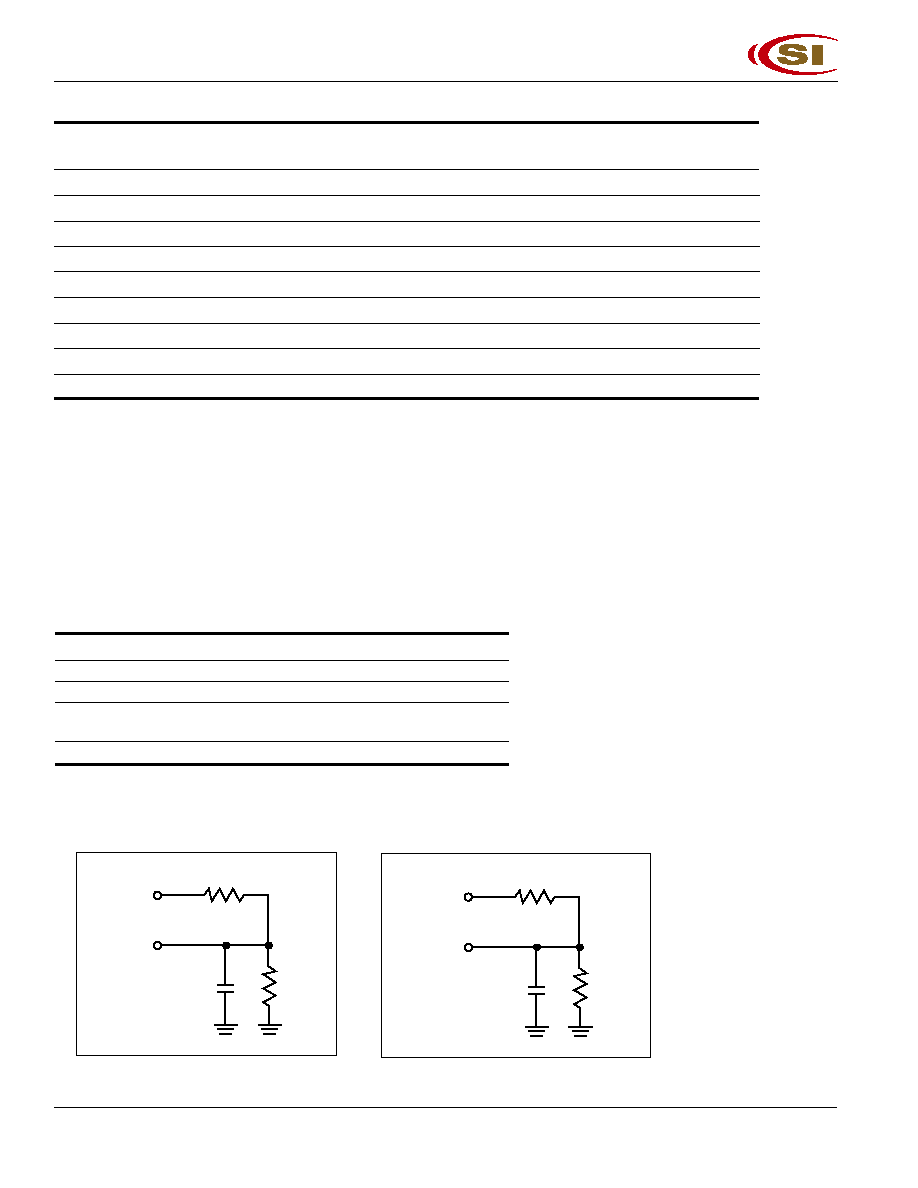
AC TEST LOADS
Figure 1.
Figure 2.
319
30 pF
Including
jig and
scope
353
OUTPUT
3.3V
319
5 pF
Including
jig and
scope
353
OUTPUT
3.3V
IS61LV5128
Integrated Circuit Solution, Inc.
5
SR027-0C
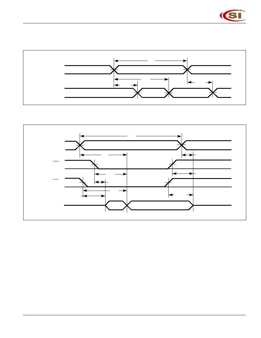
DATA VALID
PREVIOUS DATA VALID
t
AA
t
OHA
t
OHA
t
RC
D
OUT
ADDRESS
t
RC
t
OHA
t
AA
t
DOE
t
LZOE
t
ACE
t
LZCE
t
HZOE
HIGH-Z
DATA VALID
ADDRESS
OE
CE
D
OUT
t
HZCE
READ CYCLE NO. 2
(1,3)
Notes:
1. WE is HIGH for a Read Cycle.
2. The device is continuously selected. OE, CE = V
IL
.
3. Address is valid prior to or coincident with CE LOW transitions.
AC WAVEFORMS
READ CYCLE NO. 1
(1,2)