5..25V
+5V
iC-OV
THERMAL
SHUTDOWN
LOW VOLTAGE
BIAS
ERROR
TRACK1
TRACK2
2
2
1
1
TRACK3
TRACK4
TRACK5
LED-CURRENT CONTROL
DREF
DDC
MONITOR
(see TRACK2)
(see TRACK2)
(see TRACK2)
1
c2
TEST
1
c2
100nF
CB
RSET
14k
LED
RNER
10k
RLED
47
VCC
GND
LED
C5
C4
C3
C2
C1
NER
NINV
TREF
AGND
ISET
8
1
7
6
5
4
3
13
2
10
9
14
11
12
TNRF
BLCC OVC3
IS
Vref
1.0
0.5
iC-OV
5-BIT OPTO ENCODER
FEATURES
APPLICATIONS
°
High synchronism and technical reliability due to monolithic
construction plus integrated photodiodes
°
Short track pitch (600 µm)
°
Scanning with constant-light evaluation
°
Photoelectric amplifier with high cut-off frequency
°
Current comparators with hysteresis
°
Current-limited TTL-compatible push-pull outputs
°
Adjustable LED current control for constant receive power
°
Integrated 40mA driver for the LED
°
Integrated test aid
°
Output of track 1 can be inverted to change the counting
direction during Gray Code scanning
°
Overtemperature circuit-breaker with hysteresis
°
Detection and fault message when the safe operating range
is exceeded, as the result of undervoltage, over-temperature
or an LED current outside the control range
°
Low power consumption
°
Scanning with constant-light
evaluation in absolute and
multiturn rotary encoders
CHIP
3.6mm × 2.9mm
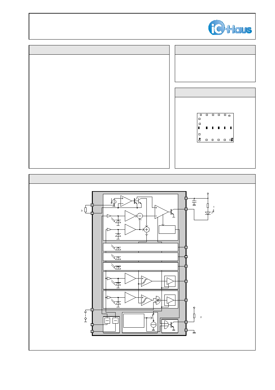
BLOCK DIAGRAM
© 2000
Rev C0
iC-Haus GmbH
Tel +49-6135-9292-0
Integrated Circuits
Fax +49-6135-9292-192
Am Kuemmerling 18, D-55294 Bodenheim
http://www.ichaus.com

iC-OV
5-BIT OPTO ENCODER
Rev C0, 2/9
DESCRIPTION
The device iC-OV is an optoelectronic encoder IC for absolute linear or angle measuring systems, e.g. glass
scales or rotary encoders.
Photodiodes, amplifiers, comparators and TTL-compatible push-pull output drivers for 5 tracks are
monolithically integrated, as well as a reference photodiode to control the LED current. The track pitch is 600
µm.
The outputs switch to high when the amplified photoelectric currents exceed a preset threshold (constant-light
evaluation). The operating point is determined by an external resistor at RSET.
This resistor also establishes the setpoint for the LED current control. The control keeps the optical receive
power constant, irrespective of the temperature or the effects of ageing. The driver stage of the LED current
control makes it possible to connect an LED with series resistor directly.
A monitoring circuit generates a fault message in the event of undervoltage, overtemperature or violation of
the LED current control range. The fault message output is busable (open collector) and low active.
Two test pins permit a complete function test (without photodiodes).
All inputs and outputs are protected against destruction by ESD. The outputs are short-circuit-proof and are
switched off in case of thermal overload.
iC-OV
5-BIT OPTO ENCODER
Rev C0, Page 3/9
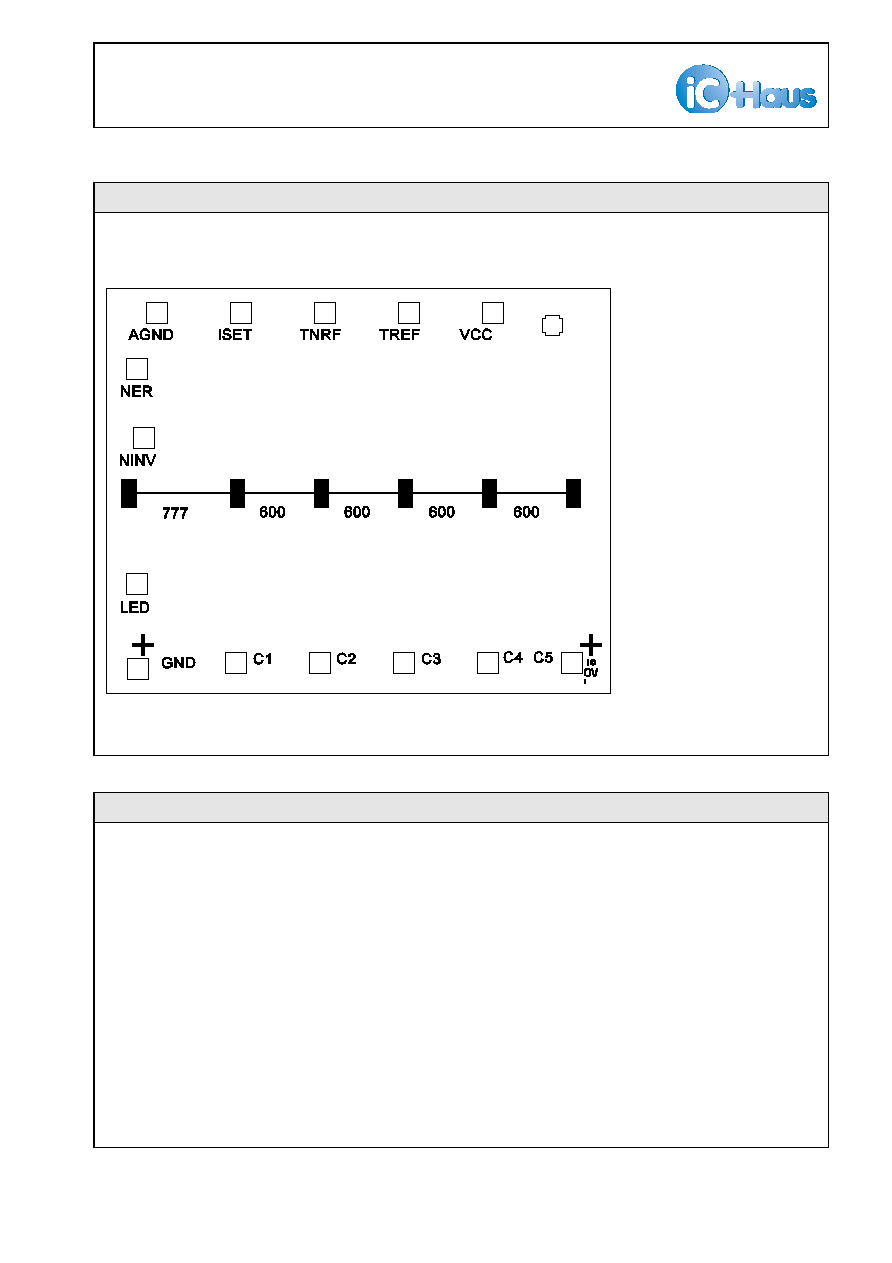
CHIP LAYOUT
dimensions in µm; chip size 3.6mm x 2.9mm
PAD DESCRIPTION
Name
Function
LED
LED Current Control Output
GND
Ground
C1
Track 1 Push-Pull Output
C2
Track 2 Push-Pull Output
C3
Track 3 Push-Pull Output
C4
Track 4 Push-Pull Output
C5
Track 5 Push-Pull Output
VCC
+5V Supply Voltage
TREF
Test Aid for photodiode DREF
TNRF
Test Aid for tracks 1 to 5 and compensation DDC
ISET
LED Current Control Setup
AGND
Reference Ground for ISET circuitry
NER
Error Message Output, low active
NINV
Track 1 Invert Mode Input, low active

iC-OV
5-BIT OPTO ENCODER
Rev C0, Page 4/9
All voltages are referenced to ground unless otherwise noted.
All currents into the device pins are positive; all currents out of the device pins are negative.
ABSOLUTE MAXIMUM RATINGS
Values beyond which damage may occur; device operation is not guaranteed.
Item
Symbol
Parameter
Conditions
Fig.
Unit
Min.
Max.
G001 VCC
Supply Voltage
0
7
V
G002 V(C)
Voltage at Outputs C1..5
0
VCC
V
G003 I(C)
Current in Outputs C1..5
V(C)< 0V or V(C)> VCC
-3
3
mA
G004 I(TNRF)
Current in TNRF
-2
1
mA
G005 I(TREF)
Current in TREF
-2
1
mA
G006 I(ISET)
Current in ISET
-2
2
mA
G007 I(AGND)
Current in AGND
-5
5
mA
G008 I(LED)
Current in LED to GND
0
50
mA
G009 I(LED)
Current in LED
V(LED)> VCC
0
3
mA
G010 V(NER)
Voltage at NER
0
30
V
G011 I(NINV)
Current in NINV
-2
2
mA
TG1 Tj
Junction Temperature
-30
125
E
C
TG2 Ts
Storage Temperature
see package specification
THERMAL DATA
Operating Conditions: VCC= 5V ±10%
Item
Symbol
Parameter
Conditions
Fig.
Unit
Min.
Typ.
Max.
T1
Ta
Operating Ambient Temperature
Range
see package specification

iC-OV
5-BIT OPTO ENCODER
Rev C0, Page 5/9
ELECTRICAL CHARACTERISTICS
Operating Conditions:
VCC= 5V ±10%, Tj= -25..125
E
C, unless otherwise noted
Item
Symbol
Parameter
Conditions
Tj
Fig.
Unit
E
C
Min.
Typ.
Max.
Total Device
001
VCC
Permissible Supply Voltage
Range
4.5
5.5
V
002
I(VCC)
Supply Current in VCC,
Outputs C1..5 hi
closed LED Control:
R(ISET/AGND)= 14k
S
,
I(LED)
.
10mA, NER= hi;
I(C1..5)= 0, I(D1..5)= 80nA
7
13
mA
003
I(VCC)
Supply Current in VCC,
Outputs C1..5 lo
closed LED Control:
R(ISET/AGND)= 14k
S
,
I(LED)
.
10mA, NER= hi;
I(C1..5)= 0, I(D1..5)
#
8nA
8
15
mA
004
fo
Cut-off Frequency,
tracks 1..5
sinusoidal waveform,
I(D1..5)= 8..80nA, I(DREF)= 80nA
200
kHz
005
)
tp()
Delay Skew C1..5
rectangular waveform,
I(D1..5)= 8..80nA, I(DREF)= 80nA
0.5
µs
Photodiodes D1..5, DREF
006
S(
8
)max
Spectral Sensitivity
8
= 850nm
0.5
A/W
007
8
ar
Spectral Application Range
Se(
8
ar)= 0.1×S(
8
)max
500
1050
nm
Photodiodes D1..5 with Amplifiers
101
Aph(D)
Radiant Sensitive Area
0.2 × 0.1
mm˛
102
CM()
Common Mode referred to
Reference Photodiode DREF
0.85
1
1.15
Difference Comparators, tracks 1..5
201
Hys
Hysteresis referred to
[I(D) + IS] /2
I(D1..5)= 0..80nA
8
12
16
%
Push-Pull Outputs C1..5
301
Vs()hi
Saturation Voltage hi
Vs()hi= VCC-V(C);
I()= -1.6mA
27
1.1
1.4
V
V
302
Vs()lo
Saturation Voltage lo
I()= 1.6mA
-25
27
85
125
0.25
0.4
0.4
0.4
0.5
V
V
V
V
303
Isc()hi
Short-Circuit Current hi
V()= 0..2.8V
27
4
9
mA
mA
304
Isc()lo
Short-Circuit Current lo
V()= 2V..VCC
27
5
10
mA
mA
305
tr()
Rise Time
C: lo
6
hi; CL= 30pF
80
260
ns
306
tf()
Fall Time
C: hi
6
lo; CL= 30pF
40
100
ns
307
Vc()hi
Clamp Voltage hi
Vc()hi= V(C)-VCC;
I()= 3mA
0.4
1.5
V
308
Vc()lo
Clamp Spannung lo
I()= -3mA
-1.5
-0.4
V
Test Aid TNRF, TREF
401
CR()
Current Ratio
I(TNRF)/I(D1..5)
test aid active,
I()= 2..200µA
200
550
800
402
CR()
Current Ratio
I(TNRF)/I(DDC),
I(TREF)/I(DREF)
test aid active,
I()= 2..200µA
400
1100
1600