2.8mm × 2.08mm
IP
IN
IP
IN
IN
IP
NI0
NI1
NI2
S0
S1
S2
ANALOG
ANALOG
OUTPUT
OUTPUT
OUTPUT
ANALOG
BIAS
OUTPUT
OUTPUT
OUTPUT
PUSH-PULL
PUSH-PULL
PUSH-PULL
DN2
DN1
DN0
TRACK 0
DP2
DP1
DP0
COMPARATOR
COMPARATOR
COMPARATOR
AMPLIFIER
AMPLIFIER
AMPLIFIER
TRACK 2
TRACK 1
VCC
GND
iC-OF
BLCC OF3C
1
8
2
3
6
4
5
7
iC-OF
3-BIT OPTO ENCODER
FEATURES
APPLICATIONS
°
Monolithic construction with integrated photodiodes ensures
excellent matching and technical reliability
°
Short track spacing of 600
F
m
°
Elimination of dark current effects through differential
scanning
°
Photocurrent amplifier with high cut-off frequency
°
Comparators with precise signal-related hysteresis
°
Current-limited push-pull outputs
°
Analog outputs as current source/sink additionally
°
Low power consumption from 5V supply voltage
°
Low board space requirements
°
Options: extended temperature range of -30..110
E
C,
customized packages, COB and reticle assembly
°
Optical position decoding for
incremental encoders using the
principle of differential scanning
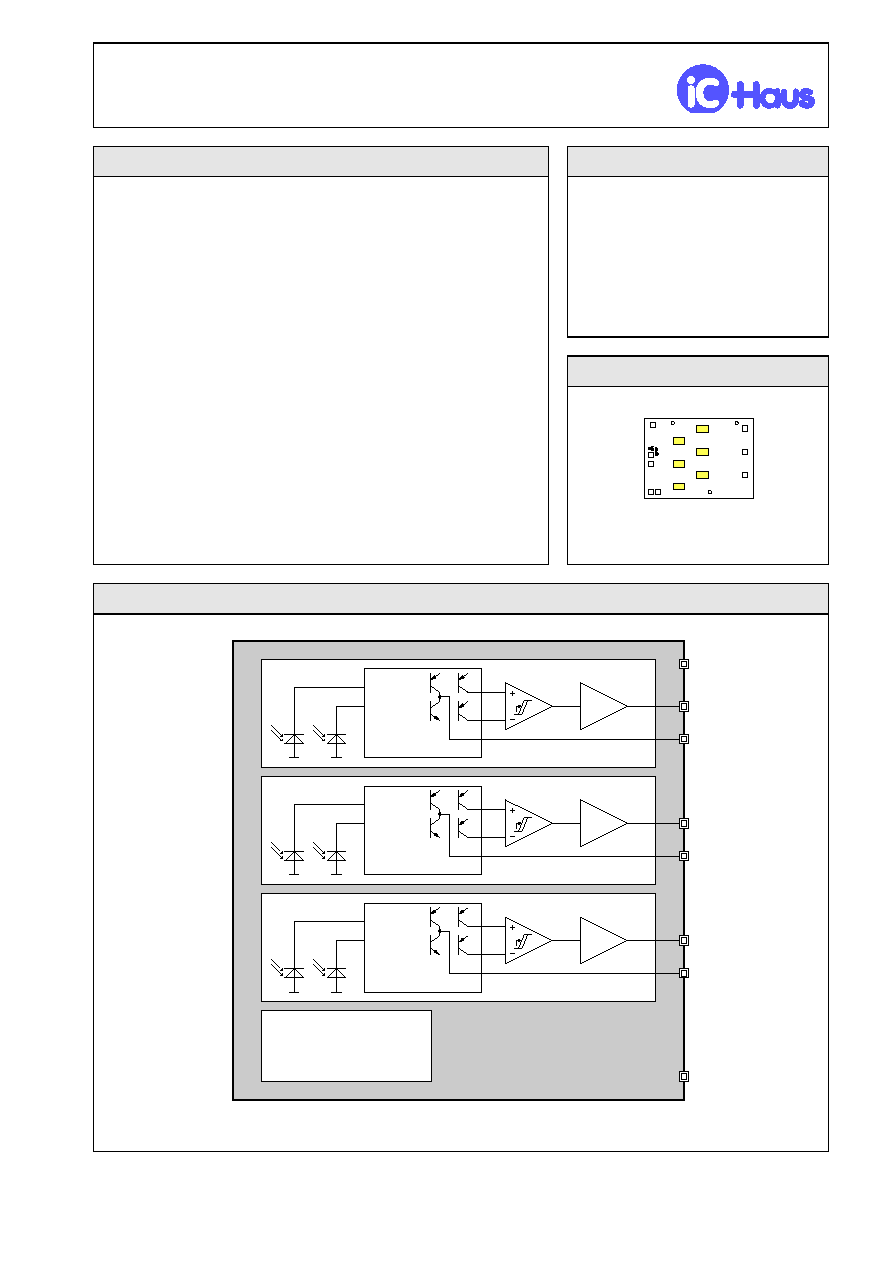
CHIP
BLOCK DIAGRAM
©2000
Rev B1
iC-Haus GmbH
Tel +49-6135-9292-0
Integrated Circuits
Fax +49-6135-9292-192
Am Kuemmerling 18, D-55294 Bodenheim
http://www.ichaus.com

iC-OF
3-BIT OPTO ENCODER
Rev B1, 2/6
DESCRIPTION
The iC-OF device is an optoelectronic detector IC for linear and angle measuring systems, such as shaft
encoders, for example.
Photodiodes, amplifiers, comparators and TTL-compatible push-pull output drivers are integrated
monolithically. Each of the 3 tracks is evaluated differentially; there are also analog outputs available.
The outputs are protected against ESD and short-circuit damage.
CHIP LAYOUT
dimensions in µm; chip size 2.8mm × 2.08mm
PAD DESCRIPTION
Name
Function
VCC
+5V Supply Voltage
NI0
Track 0 Analog Current Output
NI1
Track 1 Analog Current Output
NI2
Track 2 Analog Current Output
S0
Track 0 Push-Pull Output
S1
Track 1 Push-Pull Output
S2
Track 2 Push-Pull Output
GND
Ground

iC-OF
3-BIT OPTO ENCODER
Rev B1, 3/6
All voltages are referenced to ground unless otherwise noted.
All currents into the device pins are positive; all currents out of the device pins are negative.
ABSOLUTE MAXIMUM RATINGS
Values beyond which damage may occur; device operation is not guaranteed.
Item
Symbol
Parameter
Conditions
Fig.
Unit
Min.
Max.
G001 VCC
Supply Voltage
-0.3
6
V
G301 V(S)
Voltage at Outputs S0..2
-0.3
VCC+0.3
V
G302 I(S)
Current in Outputs S0..2
V(S)< 0V or V(S)> VCC
-3
3
mA
G501 V(NI)
Voltage at Analog Outputs NI0..2
-0.3
VCC+0.3
V
G502 I(NI)
Current in Analog Outputs NI0..2
-3
3
mA
E001 Vd()
ESD-Susceptibility at all pins
MIL-STD 883, Method 3015,
HBM 100pF/1.5k
S
2
kV
TG1 Tj
Chip Temperature
-30
125
E
C
TG2 Ts
Storage Temperature
see package specification
THERMAL DATA
Operating Conditions: VCC= 5V ±10%
Item
Symbol
Parameter
Conditions
Fig.
Unit
Min.
Typ.
Max.
T1
Ta
Operating Ambient Temperature
Range
see package specification

iC-OF
3-BIT OPTO ENCODER
Rev B1, 4/6
ELECTRICAL CHARACTERISTICS
Operating Conditions:
VCC= 5V ±10%; Tj= -30..125
E
C, unless otherwise noted.
Item
Symbol
Parameter
Conditions
Tj
Fig.
Unit
E
C
Min.
Typ.
Max.
Total Device
001
VCC
Permissible Supply Voltage
4.5
5.5
V
002
I(VCC)
Supply Current in VCC,
Outputs S0..2 hi
I(DP0..7)= 30nA, I(DN0..7)= 3nA,
I(S0..7)= 0
27
2.3
mA
003
I(VCC)
Supply Current in VCC,
Outputs S0..2 lo
I(DP0..7)= 3nA, I(DN0..7)= 30nA,
I(S0..7)= 0
27
2.3
mA
004
fo
Cut-off Frequency,
tracks 0..2
sinusoidal waveform,
I(DP0..7)= 3..30nA,
I(DN0..7)= 30..3nA
100
kHz
005
tp(D-S)
Propagation Delay
see No. 4
2.5
µs
006
fo
Propagation Delay,
tracks 0..2
sinusoidal waveform,
I(DP0..7)= 6..60nA
I(DN0..7)= 60..6nA
200
kHz
007
tp(D-S)
Propagation Delay
see No. 6
1.5
µs
Photodiodes and Amplifiers, tracks 0..2
101
Aph(D)
Radiant Sensitive Area
0.2 × 0.3
mm˛
102
S(
8
)max
Spectral Sensitivity
8
= 850nm
0.5
A/W
103
8
ar
Range of Spectral Sensitivity
Se(
8
ar)= 0.1×S(
8
)max
500
1050
nm
104
I(D)
Permissible Photocurrent
90
nA
105
CM()
Common Mode DPi to DNi
0.85
1
1.15
Difference Comparators, tracks 0..2
201
Hys
Hysteresis refered to
[I(DPi) + I(DNi)] /2
I(DPi, DNi)= 3..90nA
8
11
14
%
Push-Pull Outputs S0..2
301
Vs()hi
Saturation Voltage hi
Vs()hi= VCC-V();
I()= -40µA
-30
27
70
125
0.79
0.69
0.58
0.51
0.9
V
V
V
V
V
302
Vs()hi
Saturation Voltage hi
Vs()hi= VCC-V();
I()= -400µA
-30
27
70
125
0.90
0.83
0.74
0.68
1.0
V
V
V
V
V
303
Vs()lo
Saturation Voltage lo
I()= 1.6mA
-30
27
70
125
0.21
0.22
0.25
0.27
0.4
V
V
V
V
V
304
Isc()hi
Short-Circuit Current hi
V()= 0V..VCC-1.2V
-7
-4.6
-1.5
mA
305
Isc()lo
Short-Circuit Current lo
V()= 0.4V..VCC
1.8
7.3
13
mA
306
SRhi
Slew-Rate hi
CL()= 30pF
27
24
61
130
V/µs
V/µs
307
SRlo
Slew-Rate lo
CL()= 30pF
27
50
115
330
V/µs
V/µs
308
Vc()hi
Clamp Voltage hi
Vc()hi= V()-VCC; S= hi, I()= 3mA
0.4
1.5
V
309
Vc()lo
Clamp Voltage lo
S= lo, I()= -3mA
-1.5
-0.4
V

iC-OF
3-BIT OPTO ENCODER
Rev B1, 5/6
ELECTRICAL CHARACTERISTICS
Operating Conditions:
VCC= 5V ±10%; Tj= -30..125
E
C, unless otherwise noted.
Item
Symbol
Parameter
Conditions
Tj
Fig.
Unit
E
C
Min.
Typ.
Max.
Analog Outputs NI0..2
501
CR()
Current Ratio
I(NIi) / (I(DPi)-I(DNi))
V(NIi)= 0.3V..VCC-1.2V,
I(DPi)= 3..90nA, I(DNi)= 90..3nA
27
550
720
850
502
I0()
Leakage Current
V(NI)= 0.3V..VCC-1.2V,
I(DPi,DNi)= 0
-1.5
1.5
µA
503
fo()
Cut-off Frequency
V(NIi)= constant,
sinussoidal waveform,
I(DPi)= 3..30nA, I(DNi)= 30..3nA
100
kHz
504
fo()
Cut-off Frequency
V(NIi)= constant,
sinussoidal waveform,
I(DPi)= 6..60nA, I(DNi)= 60..6nA
200
kHz
505
fo()
Cut-off Frequency
R(VCC/NIi)= 50k
S
,
R(NIi/GND)= 50k
S
, CL()= 30pF
50
80
kHz
506
Vc(S)hi
Clamp Voltage hi
Vc()hi= V()-VCC; I()= 3mA
0.4
1.5
V
507
Vc(S)lo
Clamp Voltage lo
I()= -3mA
-1.5
-0.4
V
APPLICATIONS INFORMATION
Wiring of the analog outputs NI0..2
The analog outputs each consist of two current sources in a push-pull configuration. One of these works towards
GND as a sink, the other works as a source coming from VCC. The voltage swing at the output pins NI0..2 is
determined by the external wiring - the saturation voltage of the current sources must be taken into account.
The simplest configuration is to connect the outputs to a voltage divider consisting of two resistors, wired from
VCC against GND (with 50k
S
respectively, for example). Any resulting load capacities can reduce the cutoff
frequency of the analog signals.
In view of the suppression of the supply voltage, however it may be preferable to use an op-amp as a current-
voltage converter (transconductance amplifier) if the reference potential is suitably stable.