
This document is a general product description and is subject to change without notice. Hynix does not assume any responsibility for
use of circuits described. No patent licenses are implied.
Rev. 0.5/ Jul. 2006
1
HY27UF084G2M Series
4Gbit (512Mx8bit) NAND Flash
4Gb NAND FLASH
HY27UF084G2M

Rev. 0.5 / Jul. 2006
2
HY27UF084G2M Series
4Gbit (512Mx8bit) NAND Flash
Document Title
4Gbit (512Mx8bit) NAND Flash Memory
Revision History
Revision
No.
History
Draft Date
Remark
0.0
Initial Draft.
Dec. 2004
Initial
0.1
1) Add ULGA Package.
- Figures & texts are added.
2) Add Read ID Table
3) Correct the test Conditions (DC Characteristics table)
3) Change AC Conditions table
4) Add tWW parameter ( tWW = 100ns, min)
- Texts & Figures are added.
- tWW is added in AC timing characteristics table.
4) Edit System Interface Using CE don't care.
5) Add Marking Information.
6) Correct Address Cycle Map.
7) Correct PKG dimension (TSOP PKG)
8) Delete the 1.8V device's features.
Aug. 08. 2005
Preliminary
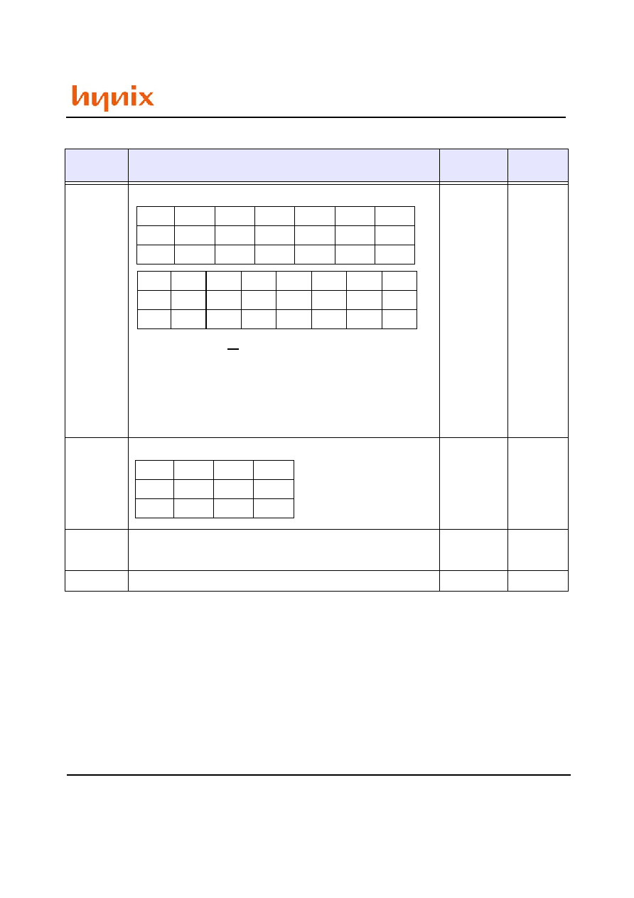
Test Conditions (
I
LI,
I
LO
)
Before
VIN=VOUT=0 to 3.6V
After VIN=VOUT=0 to Vcc (max)
CP
Before
0.050
After
0.100
Rev. 0.5 / Jul. 2006
3
HY27UF084G2M Series
4Gbit (512Mx8bit) NAND Flash
Revision History
-Continued-
Revision
No.
History
Draft Date
Remark
0.2
1) Change AC Characteristics
2) Add tCRRH (100ns, Min)
- tCRRH : Cache Read RE High
3) Change 3rd Read ID
- 3rd Read ID is changed to 80h
- 3rd Byte of Device Identifier Table is added.
4) Change NOP
- Number of partial Program Cycle in the same page is changed to 4.
Oct. 08. 2005
Preliminary
0.3
1) Change AC Characteristics
Nov. 16. 2005 Preliminary
0.4
1) Add ECC algorithm. (1bit/512bytes)
2) Change NOP
3) Correct Read ID naming
Jun. 20. 2006
Preliminary
0.5
1) Delet Preliminary.
Jul. 10. 2006
tR
tAR
tREA
tRHZ
tCHZ
tCEA
Before
20
10
18
30
30
25
After
25
15
20
50
50
35
tCLS
tWP
tDS
tWC
tADL
tRP
tRC
Before
12
12
12
25
70
12
25
After
15
15
15
30
100
15
30
tREA
tCEA
tCS
Before
20
35
20
After
25
30
25

Rev. 0.5 / Jul. 2006
4
HY27UF084G2M Series
4Gbit (512Mx8bit) NAND Flash
FEATURES SUMMARY
HIGH DENSITY NAND FLASH MEMORIES
- Cost effective solutions for mass storage applications
NAND INTERFACE
- x8 width.
- Multiplexed Address/ Data
- Pinout compatibility for all densities
SUPPLY VOLTAGE
- 3.3V device: VCC = 2.7 to 3.6V : HY27UF084G2M
Memory Cell Array
= (2K+ 64) Bytes x 64 Pages x 4,096 Blocks
PAGE SIZE
- x8 device : (2K + 64 spare) Bytes
: HY27UF084G2M
BLOCK SIZE
- x8 device: (128K + 4K spare) Bytes
PAGE READ / PROGRAM
- Random access: 25us (max.)
- Sequential access: 30ns (min.)
- Page program time: 200us (typ.)
COPY BACK PROGRAM MODE
- Fast page copy without external buffering
CACHE PROGRAM MODE
- Internal Cache Register to improve the program
throughput
FAST BLOCK ERASE
- Block erase time: 2ms (Typ.)
STATUS REGISTER
ELECTRONIC SIGNATURE
- 1st cycle : Manufacturer Code
- 2nd cycle: Device Code
CHIP ENABLE DON'T CARE
- Simple interface with microcontroller
AUTOMATIC PAGE 0 READ AT POWER-UP OPTION
- Boot from NAND support
- Automatic Memory Download
SERIAL NUMBER OPTION
HARDWARE DATA PROTECTION
- Program/Erase locked during Power transitions
DATA INTEGRITY
- 100,000 Program/Erase cycles (with 1bit/512byte ECC)
- 10 years Data Retention
PACKAGE
- HY27UF084G2M-T(P)
: 48-Pin TSOP1 (12 x 20 x 1.2 mm)
- HY27UF084G2M-T (Lead)
- HY27UF084G2M-TP (Lead Free)
- HY27UF084G2M-UP
: 52-ULGA (12 x 17 x 0.65 mm)
- HY27UF084G2M-UP (Lead Free)

Rev. 0.5 / Jul. 2006
5
HY27UF084G2M Series
4Gbit (512Mx8bit) NAND Flash
1. SUMMARY DESCRIPTION
The HYNIX HY27UF084G2M series is a 512Mx8bit with spare 16Mx8 bit capacity. The device is offered in 3.3V Vcc
Power Supply.
Its NAND cell provides the most cost-effective solution for the solid state mass storage market.
The memory is divided into blocks that can be erased independently so it is possible to preserve valid data while old
data is erased.
The device contains 4096 blocks, composed by 64 pages consisting in two NAND structures of 32 series connected
Flash cells.
A program operation allows to write the 2112-byte page in typical 200us and an erase operation can be performed in
typical 2ms on a 128K-byte(X8 device) block.
Data in the page mode can be read out at 30ns cycle time per byte. The I/O pins serve as the ports for address and
data input/output as well as command input. This interface allows a reduced pin count and easy migration towards dif-
ferent densities, without any rearrangement of footprint.
Commands, Data and Addresses are synchronously introduced using CE, WE, ALE and CLE input pin.
The on-chip Program/Erase Controller automates all program and erase functions including pulse repetition, where
required, and internal verification and margining of data.
The modifying can be locked using the WP input pin or using the extended lock block feature described later.
The output pin R/B (open drain buffer) signals the status of the device during each operation. In a system with multi-
ple memories the R/B pins can be connected all together to provide a global status signal.
Even the write-intensive systems can take advantage of the HY27UF084G2M extended reliability of 100K program/
erase cycles by providing ECC (Error Correcting Code) with real time mapping-out algorithm.
The chip could be offered with the CE don't care function. This function allows the direct download of the code from
the NAND Flash memory device by a microcontroller, since the CE transitions do not stop the read operation.
The copy back function allows the optimization of defective blocks management: when a page program operation fails
the data can be directly programmed in another page inside the same array section without the time consuming serial
data insertion phase.
The cache program feature allows the data insertion in the cache register while the data register is copied into the
flash array. This pipelined program operation improves the program throughput when long files are written inside the
memory.
A cache read feature is also implemented. This feature allows to dramatically improve the read throughput when con-
secutive pages have to be streamed out.
This device includes also extra features like OTP/Unique ID area, Block Lock mechanism, Automatic Read at Power Up,
Read ID2 extension.
The HYNIX HY27UF084G2M series is available in 48 - TSOP1 12 x 20 mm, 52-ULGA 12 x 17 mm.
1.1 Product List
PART NUMBER
ORIZATION
VCC RANGE
PACKAGE
HY27UF084G2M
x8
2.7V - 3.6 Volt
48TSOP1 / 52-ULGA

Rev. 0.5 / Jul. 2006
6
HY27UF084G2M Series
4Gbit (512Mx8bit) NAND Flash
Figure1: Logic Diagram
IO7 - IO0
Data Input / Outputs
CLE
Command latch enable
ALE
Address latch enable
CE
Chip Enable
RE
Read Enable
WE
Write Enable
WP
Write Protect
R/B
Ready / Busy
Vcc
Power Supply
Vss
Ground
NC
No Connection
PRE
Power-On Read Enable, Lock Unlock
Table 1: Signal Names

Rev. 0.5 / Jul. 2006
7
HY27UF084G2M Series
4Gbit (512Mx8bit) NAND Flash
Figure 2. 48TSOP1 Contactions, x8 Device
Rev. 0.5 / Jul. 2006
8
HY27UF084G2M Series
4Gbit (512Mx8bit) NAND Flash
Figure 3. 52-ULGA Contactions, x8 Device (Top view through package)

Rev. 0.5 / Jul. 2006
9
HY27UF084G2M Series
4Gbit (512Mx8bit) NAND Flash
1.2 PIN DESCRIPTION
Pin Name
Description
IO0-IO7
DATA INPUTS/OUTPUTS
The IO pins allow to input command, address and data and to output data during read / program
operations. The inputs are latched on the rising edge of Write Enable (WE). The I/O buffer float to
High-Z when the device is deselected or the outputs are disabled.
CLE
COMMAND LATCH ENABLE
This input activates the latching of the IO inputs inside the Command Register on the Rising edge of
Write Enable (WE).
ALE
ADDRESS LATCH ENABLE
This input activates the latching of the IO inputs inside the Address Register on the Rising edge of
Write Enable (WE).
CE
CHIP ENABLE
This input controls the selection of the device. When the device is busy CE low does not deselect the
memory.
WE
WRITE ENABLE
This input acts as clock to latch Command, Address and Data. The IO inputs are latched on the rise
edge of WE.
RE
READ ENABLE
The RE input is the serial data-out control, and when active drives the data onto the I/O bus. Data is
valid tREA after the falling edge of RE which also increments the internal column address counter by
one.
WP
WRITE PROTECT
The WP pin, when Low, provides an Hardware protection against undesired modify (program / erase)
operations.
R/B
READY BUSY
The Ready/Busy output is an Open Drain pin that signals the state of the memory.
VCC
SUPPLY VOLTAGE
The VCC supplies the power for all the operations (Read, Write, Erase).
VSS
GROUND
NC
NO CONNECTION
PRE
To Enable Power On Auto Read. When PRE is a logic high, Power on Auto Read mode is enabled, and
when PRE is a logic low, Power Auto Read mode is disabled. Power On Auto Read mode is available
only on 3.3V device.
Not using POWER-ON AUTO-READ, connect it Vss or leave it NC.
Table 2: Pin Description
NOTE:
1. A 0.1uF capacitor should be connected between the VCC Supply Voltage pin and the VSS Ground pin to decouple
the current surges from the power supply. The PCB track widths must be sufficient to carry the currents required
during program and erase operations.

Rev. 0.5 / Jul. 2006
10
HY27UF084G2M Series
4Gbit (512Mx8bit) NAND Flash
IO0
IO1
IO2
IO3
IO4
IO5
IO6
IO7
1st Cycle
A0
A1
A2
A3
A4
A5
A6
A7
2nd Cycle
A8
A9
A10
A11
L
(1)
L
(1)
L
(1)
L
(1)
3rd Cycle
A12
A13
A14
A15
A16
A17
A18
A19
4th Cycle
A20
A21
A22
A23
A24
A25
A26
A27
5th Cycle
A28
A29
L
(1)
L
(1)
L
(1)
L
(1)
L
(1)
L
(1)
Table 3: Address Cycle Map(x8)
NOTE:
1. L must be set to Low.
FUNCTION
1st CYCLE
2nd CYCLE
3rd CYCLE
Acceptable command
during busy
READ 1
00h
30h
-
READ FOR COPY-BACK
00h
35h
-
READ ID
90h
-
-
RESET
FFh
-
-
Yes
PAGE PROGRAM (start)
80h
10h
-
COPY BACK PGM (start)
85h
10h
-
CACHE PROGRAM
80h
15h
-
BLOCK ERASE
60h
D0h
-
READ STATUS REGISTER
70h
-
-
Yes
RANDOM DATA INPUT
85h
-
-
RANDOM DATA OUTPUT
05h
E0h
-
CACHE READ START
00h
31h
-
CACHE READ EXIT
34h
-
-
LOCK BLOCK
2Ah
-
-
LOCK TIGHT
2Ch
-
-
UNLOCK (start area)
23h
-
-
UNLOCK (end area)
24h
-
-
READ LOCK STATUS
7Ah
-
-
Table 4: Command Set

Rev. 0.5 / Jul. 2006
11
HY27UF084G2M Series
4Gbit (512Mx8bit) NAND Flash
CLE
ALE
CE
WE
RE
WP
MODE
H
L
L
Rising
H
X
Read Mode
Command Input
L
H
L
Rising
H
X
Address Input(5 cycles)
H
L
L
Rising
H
H
Write Mode
Command Input
L
H
L
Rising
H
H
Address Input(5 cycles)
L
L
L
Rising
H
H
Data Input
L
L
L
(1)
H
Falling
X
Sequential Read and Data Output
L
L
L
H
H
X
During Read (Busy)
X
X
X
X
X
H
During Program (Busy)
X
X
X
X
X
H
During Erase (Busy)
X
X
X
X
X
L
Write Protect
X
X
H
X
X
0V/Vcc
Stand By
Table 5: Mode Selection
NOTE:
1. With the CE high during latency time does not stop the read operation

Rev. 0.5 / Jul. 2006
12
HY27UF084G2M Series
4Gbit (512Mx8bit) NAND Flash
2. BUS OPERATION
There are six standard bus operations that control the device. These are Command Input, Address Input, Data Input,
Data Output, Write Protect, and Standby.
Typically glitches less than 5 ns on Chip Enable, Write Enable and Read Enable are ignored by the memory and do not
affect bus operations.
2.1 Command Input.
Command Input bus operation is used to give a command to the memory device. Command are accepted with Chip
Enable low, Command Latch Enable High, Address Latch Enable low and Read Enable High and latched on the rising
edge of Write Enable. Moreover for commands that starts a modifying operation (write/erase) the Write Protect pin
must be high. See figure 5 and table 12 for details of the timings requirements. Command codes are always applied on
IO7:0, disregarding the bus configuration (X8).
2.2 Address Input.
Address Input bus operation allows the insertion of the memory address. To insert the 29 addresses needed to access
the 4Gbit 5 clock cycles are needed. Addresses are accepted with Chip Enable low, Address Latch Enable High, Com-
mand Latch Enable low and Read Enable high and latched on the rising edge of Write Enable. Moreover for commands
that starts a modify operation (write/erase) the Write Protect pin must be high. See figure 6 and table 12 for details of
the timings requirements. Addresses are always applied on IO7:0, disregarding the bus configuration (X8).
2.3 Data Input.
Data Input bus operation allows to feed to the device the data to be programmed. The data insertion is serially and
timed by the Write Enable cycles. Data are accepted only with Chip Enable low, Address Latch Enable low, Command
Latch Enable low, Read Enable High, and Write Protect High and latched on the rising edge of Write Enable. See figure
7 and table 12 for details of the timings requirements.
2.4 Data Output.
Data Output bus operation allows to read data from the memory array and to check the status register content, the
lock status and the ID data. Data can be serially shifted out toggling the Read Enable pin with Chip Enable low, Write
Enable High, Address Latch Enable low, and Command Latch Enable low. See figures 8,10,11 and table 12 for details
of the timings requirements.
2.5 Write Protect.
Hardware Write Protection is activated when the Write Protect pin is low. In this condition modify operation do not
start and the content of the memory is not altered. Write Protect pin is not latched by Write Enable to ensure the pro-
tection even during the power up.
2.6 Standby.
In Standby mode the device is deselected, outputs are disabled and Power Consumption is reduced.

Rev. 0.5 / Jul. 2006
13
HY27UF084G2M Series
4Gbit (512Mx8bit) NAND Flash
3. DEVICE OPERATION
3.1 Page Read.
Upon initial device power up, the device defaults to Read mode. This operation is also initiated by writing 00h and 30h
to the command register along with five address cycles. In two consecutive read operations, the second one doesn't'
need 00h command, which five address cycles and 30h command initiates that operation. Two types of operations are
available : random read, serial page read. The random read mode is enabled when the page address is changed. The
2112 bytes (X8 device) of data within the selected page are transferred to the data registers in less than 25us(tR). The
system controller may detect the completion of this data transfer (tR) by analyzing the output of R/B pin. Once the
data in a page is loaded into the data registers, they may be read out in 30ns cycle time by sequentially pulsing RE.
The repetitive high to low transitions of the RE clock make the device output the data starting from the selected col-
umn address up to the last column address.
The device may output random data in a page instead of the consecutive sequential data by writing random data out-
put command.
The column address of next data, which is going to be out, may be changed to the address which follows random data
output command.
Random data output can be operated multiple times regardless of how many times it is done in a page.
3.2 Page Program.
The device is programmed basically by page, but it does allow multiple partial page programming of a word or consec-
utive bytes up to 2112 (X8 device) , in a single page program cycle. The number of consecutive partial page program-
ming operation within the same page without an intervening erase operation must not exceed 4 times for main array
(X8 device:1time/512byte) and 4 times for spare array (X8 device:1time/16byte).
The addressing should be done in sequential order in a block
1
. A page program cycle consists of a serial data
loading period in which up to 2112bytes (X8 device) of data may be loaded into the data register, followed by a non-
volatile programming period where the loaded data is programmed into the appropriate cell.
The serial data loading period begins by inputting the Serial Data Input command (80h), followed by the five cycle
address inputs and then serial data. The words other than those to be programmed do not need to be loaded. The
device supports random data input in a page. The column address of next data, which will be entered, may be
changed to the address which follows random data input command (85h). Random data input may be operated multi-
ple times regardless of how many times it is done in a page.
The Page Program confirm command (10h) initiates the programming process. Writing 10h alone without previously
entering the serial data will not initiate the programming process. The internal write state controller automatically exe-
cutes the algorithms and timings necessary for program and verify, thereby freeing the system controller for other
tasks. Once the program process starts, the Read Status Register command may be entered to read the status register.
The system controller can detect the completion of a program cycle by monitoring the R/B output, or the Status bit (I/
O 6) of the Status Register. Only the Read Status command and Reset command are valid while programming is in
progress. When the Page Program is complete, the Write Status Bit (I/O 0) may be checked. The internal write verify
detects only errors for "1"s that are not successfully programmed to "0"s. The command register remains in Read Sta-
tus command mode until another valid command is written to the command register. Figure 13 details the sequence.

Rev. 0.5 / Jul. 2006
14
HY27UF084G2M Series
4Gbit (512Mx8bit) NAND Flash
3.3 Block Erase.
The Erase operation is done on a block basis. Block address loading is accomplished in three cycles initiated by an
Erase Setup command (60h). Only address A18 to A29 (X8) is valid while A12 to A17 (X8) is ignored. The Erase Con-
firm command (D0h) following the block address loading initiates the internal erasing process. This two-step sequence
of setup followed by execution command ensures that memory contents are not accidentally erased due to external
noise conditions.
At the rising edge of WE after the erase confirm command input, the internal write controller handles erase and erase-
verify.
Once the erase process starts, the Read Status Register command may be entered to read the status register. The sys-
tem controller can detect the completion of an erase by monitoring the R/B output, or the Status bit (I/O 6) of the Sta-
tus Register. Only the Read Status command and Reset command are valid while erasing is in progress. When the
erase operation is completed, the Write Status Bit (I/O 0) may be checked.
Figure 17 details the sequence.
3.4 Copy-Back Program.
The copy-back program is configured to quickly and efficiently rewrite data stored in one page without utilizing an
external memory. Since the time-consuming cycles of serial access and re-loading cycles are removed, the system per-
formance is improved. The benefit is especially obvious when a portion of a block is updated and the rest of the block
also need to be copied to the newly assigned free block. The operation for performing a copy-back program is a
sequential execution of page-read without serial access and copying-program with the address of destination page. A
read operation with "35h" command and the address of the source page moves the whole 2112byte (X8 device) data
into the internal data buffer. As soon as the device returns to Ready state, Copy Back command (85h) with the address
cycles of destination page may be written. The Program Confirm command (10h) is required to actually begin the pro-
gramming operation. Data input cycle for modifying a portion or multiple distant portions of the source page is allowed
as shown in Figure 15.
"When there is a program-failure at Copy-Back operation, error is reported by pass/fail status. But, if
Copy-Back operations are accumulated over time, bit error due to charge loss is not checked by external
error detection/correction scheme. For this reason, two bit error correction is recommended for the use
of Copy-Back operation."
Figure 15 shows the command sequence for the copy-back operation.
The Copy Back Program operation requires three steps:
1. The source page must be read using the Read A command (one bus write cycle to setup the command and then
5 bus write cycles to input the source page address). This operation copies all 2KBytes from the page into the Page
Buffer.
2. When the device returns to the ready state (Ready/Busy High), the second bus write cycle of the command is
given with the 5bus cycles to input the target page address. The value for A29 from second to the last page address
must be same as the value given to A29 in first address.
3. Then the confirm command is issued to start the P/E/R Controller.

Rev. 0.5 / Jul. 2006
15
HY27UF084G2M Series
4Gbit (512Mx8bit) NAND Flash
3.5 Read Status Register.
The device contains a Status Register which may be read to find out whether read, program or erase operation is com-
pleted, and whether the program or erase operation is completed successfully. After writing 70h command to the com-
mand register, a read cycle outputs the content of the Status Register to the I/O pins on the falling edge of CE or RE,
whichever occurs last. This two line control allows the system to poll the progress of each device in multiple memory
connections even when R/B pins are common-wired. RE or CE does not need to be toggled for updated status. Refer
to table 13 for specific Status Register definitions. The command register remains in Status Read mode until further
commands are issued to it. Therefore, if the status register is read during a random read cycle, the read command
(00h) should be given before starting read cycles. See figure 12 for details of the Read Status operation.
3.6 Read ID.
The device contains a product identification mode, initiated by writing 90h to the command register, followed by an
address input of 00h. Four read cycles sequentially output the manufacturer code (ADh), and the device code and 3rd
cycle ID, 4th cycle ID, respectively. The command register remains in Read ID mode until further commands are
issued to it. Figure 20 shows the operation sequence, while tables 15 explain the byte meaning.
3.7 Reset.
The device offers a reset feature, executed by writing FFh to the command register. When the device is in Busy state
during random read, program or erase mode, the reset operation will abort these operations. The contents of memory
cells being altered are no longer valid, as the data will be partially programmed or erased. The command register is
cleared to wait for the next command, and the Status Register is cleared to value E0h when WP is high. Refer to table
13 for device status after reset operation. If the device is already in reset state a new reset command will not be
accepted by the command register. The R/B pin transitions to low for tRST after the Reset command is written. Refer
to figure 30.

Rev. 0.5 / Jul. 2006
16
HY27UF084G2M Series
4Gbit (512Mx8bit) NAND Flash
3.8 Cache Program.
Cache Program is an extension of Page Program, which is executed with 2112byte (X8 device) data registers, and is
available only within a block. Since the device has 1 page of cache memory, serial data input may be executed while
data stored in data register are programmed into memory cell. After writing the first set of data up to 2112byte (X8
device) into the selected cache registers, Cache Program command (15h) instead of actual Page Program (10h) is
input to make cache registers free and to start internal program operation. To transfer data from cache registers to
data registers, the device remains in Busy state for a short period of time (tCBSY) and has its cache registers ready for
the next data-input while the internal programming gets started with the data loaded into data registers. Read Status
command (70h) may be issued to find out when cache registers become ready by polling the Cache-Busy status bit (I/
O 6). Pass/fail status of only the previous page is available upon the return to Ready state. When the next set of data
is input with the Cache Program command, tCBSY is affected by the progress of pending internal programming. The
programming of the cache registers is initiated only when the pending program cycle is finished and the data registers
are available for the transfer of data from cache registers. The status bit (I/O5) for internal Ready/Busy may be polled
to identify the completion of internal programming.
If the system monitors the progress of programming only with R/B, the last page of the target programming sequence
must be programmed with actual Page Program command (10h). If the Cache Program command (15h) is used
instead, status bit (I/O5) must be polled to find out when the last programming is actually finished before starting
other operations such as read. Pass/fail status is available in two steps. I/O 1 returns with the status of the previous
page upon Ready or I/O6 status bit changing to "1", and later I/O 0 with the status of current page upon true Ready
(returning from internal programming) or I/O 5 status bit changing to "1". I/O 1 may be read together when I/O 0 is
checked. See figure 16 for more details.
NOTE : Since programming the last page does not employ caching, the program time has to be that of Page Program.
However, if the previous program cycle with the cache data has not finished, the actual program cycle of the
last page is initiated only after completion of the previous cycle, which can be expressed as the following
formula.
tPROG= Program time for the last page+ Program time for the ( last -1 )th page
- (Program command cycle time + Last page data loading time)
The value for A29 from second to the last page address must be same as the value given to A29 in first address.

Rev. 0.5 / Jul. 2006
17
HY27UF084G2M Series
4Gbit (512Mx8bit) NAND Flash
3.9 Cache Read
Cache read operation allows automatic download of consecutive pages, up to the whole device. Immediately after 1st
latency end, while user can start reading out data, device internally starts reading following page.
Start address of 1st page is at page start (A<10:0>=00h), after 1st latency time (tr) , automatic data download will
be uninterrupted. In fact latency time is 25us, while download of a page require at least 100us for x8 device.
Cache read operation command is like standard read, except for confirm code (30h for standard read, 31h for cache
read) user can check operation status using :
- R/B ( `0' means latency ongoing, download not possible, `1' means download of n page possible, even if device
internally is active on n+1 page
- Status register (SR<6> behave like R/B, SR<5> is `0' when device is internally reading and `1' when device is idle)
To exit cache read operation a cache read exit command (34h) must be issued. this command can be given any time
(both device idle and reading).
If device is active (SR<5>=0) it will go idle within 5us, while if it is not active, device itself will go busy for a time
shorter then tRBSY before becoming again idle and ready to accept any further commands.
If user arrives reading last byte/word of the memory array, then has to stop by giving a cache read exit command.
Random data output is not available in cache read.
Cache read operation must be done only block by block if system needs to avoid reading also from invalid blocks.

Rev. 0.5 / Jul. 2006
18
HY27UF084G2M Series
4Gbit (512Mx8bit) NAND Flash
4. OTHER FEATURES
4.1 Data Protection.
The device is designed to offer protection from any involuntary program/erase during power-transitions. An internal
voltage detector disables all functions whenever Vcc is below about 2V(3.3V device). WP pin provides hardware pro-
tection and is recommended to be kept at VIL during power-up and power-down. A recovery time of minimum 10us is
required before internal circuit gets ready for any command sequences as shown in Figure 32. The two-step command
sequence for program/erase provides additional software protection.
If the power is dropped during the ready read/write/erase operation, Power protection function may not guaranteed
the data. Power protection function is only available during the power on/off sequence.
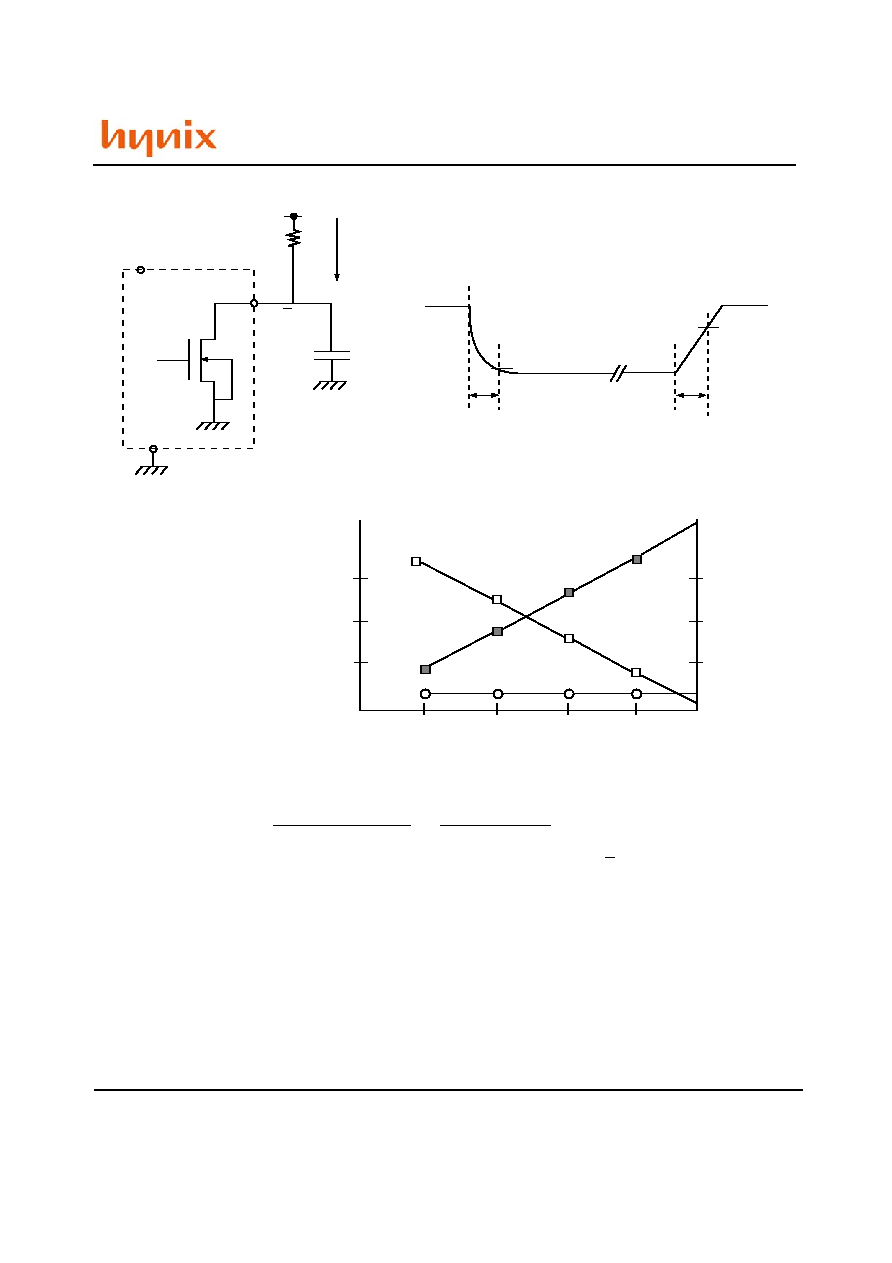
4.2 Ready/Busy.
The device has a Ready/Busy output that provides method of indicating the completion of a page program, erase,
copy-back, cache program and random read completion. The R/B pin is normally high and goes to low when the device
is busy (after a reset, read, program, erase operation). It returns to high when the internal controller has finished the
operation. The pin is an open-drain driver thereby allowing two or more R/B outputs to be Or-tied. Because pull-up
resistor value is related to tr(R/B) and current drain during busy (Ibusy), an appropriate value can be obtained with
the following reference chart (Fig 31). Its value can be determined by the following guidance.
4.3 Lock Block Feature
In high state of PRE pin, Block lock mode is enabled, otherwise it is regarded as NAND Flash without
PRE pin.
Block Lock mode is enabled while PRE pin state is high, which is to offer protection features for NAND Flash data. The
Block Lock mode is divided into Unlock, Lock, Lock-tight operation. Consecutive blocks protects data allows those
blocks to be locked or lock-tighten with no latency. This block lock scheme offers two levels of protection. The first
allows software control (command input method) of block locking that is useful for frequently changed data blocks,
while the second requires hardware control (WP low pulse input method) before locking can be changed that is useful
for protecting infrequently changed code blocks. The followings summarized the locking functionality.
- All blocks are in a locked state on power-up. Unlock sequence can unlock the locked blocks.
- The Lock-tight command locks blocks and prevents from being unlocked. Lock-tight state can be returned to lock
state only by Hardware control(WP low pulse input).
1. Block lock operation
1) Lock
- Command Sequence: Lock block Command (2Ah). See Fig. 23.
- All blocks default to locked by power-up and Hardware control (WP low pulse input)
- Partial block lock is not available; Lock block operation is based on all block unit
- Unlocked blocks can be locked by using the Lock block command, and a lock block's status can be changed to
unlock or lock-tight using the appropriate commands
- On the program or erase operation in Locked or Lock-tighten block, Busy state holds 5~10us(tLBSY)

Rev. 0.5 / Jul. 2006
19
HY27UF084G2M Series
4Gbit (512Mx8bit) NAND Flash
2) Unlock
- Command Sequence: Unlock block Command (23h) + Start block address + Command (24h) + End block address.
See Fig. 25.
- Unlocked blocks can be programmed or erased.
- An unlocked block's status can be changed to the locked or lock-tighten state using the appropriate sequence of
commands.
- Only one consecutive area can be released to unlock state from lock state; Unlocking multi area is not available.
- Start block address must be nearer to the logical LSB (Least Significant Bit) than End block address.
- One block is selected for unlocking block when Start block address is same as End block address.
3) Lock-tight
- Command Sequence: Lock-tight block Command (2Ch). See Fig. 26.
- Lock-tighten blocks offer the user an additional level of write protection beyond that of a regular lock block. A block
that is lock-tighten can't have its state changed by software control, only by hardware control (WP low pulse
input); Unlocking multi area is not available
- Only locked blocks can be lock-tighten by lock-tight command.
- On the program or erase operation in Locked or Lock-tighten block, Busy state holds 5~10us(tLBSY)
2. Block lock Status Read
Block Lock Status can be read on a block basis to find out whether designated block is available to be programmed or
erased. After writing 7Ah command to the command register and block address to be checked, a read cycle outputs
the content of the Block Lock Status Register to the I/O pins on the falling edge of CE or RE, whichever occurs last. RE
or CE does not need to be toggled for updated status. Block Lock Status Read is prohibited while the device is busy
state.
Refer to table 18 for specific Status Register definitions. The command register remains in Block Lock Status Read
mode until further commands are issued to it.
In high state of LOCKPRE pin, write protection status can be checked by Block Lock Status Read (7Ah)
while in low state by Status Read (70h).
4.4 Power-On Auto-Read
The device is designed to offer automatic reading of the first page without command and address input sequence dur-
ing power-on.
An internal voltage detector enables auto-page read functions when Vcc reaches about 1.8V. Auto-page read function
is enabled only when Vcc pin is logic high state. Serial access may be done after power-on without latency.
Power-On Auto Read mode is available only on 3.3V device.

Rev. 0.5 / Jul. 2006
20
HY27UF084G2M Series
4Gbit (512Mx8bit) NAND Flash
Parameter
Symbol
Min
Typ
Max
Unit
Valid Block Number
N
VB
4016
4096
Blocks
Table 6: Valid Blocks Number
NOTE:
1. The 1st block is guaranteed to be a valid block up to 1K cycles with ECC. (1bit/512bytes)

Rev. 0.5 / Jul. 2006
21
HY27UF084G2M Series
4Gbit (512Mx8bit) NAND Flash
Symbol
Parameter
Value
Unit
3.3V
T
A
Ambient Operating Temperature (Commercial Temperature Range)
0 to 70
Ambient Operating Temperature (Extended Temperature Range)
-25 to 85
Ambient Operating Temperature (Industry Temperature Range)
-40 to 85
T
BIAS
Temperature Under Bias
-50 to 125
T
STG
Storage Temperature
-65 to 150
V
IO(2)
Input or Output Voltage
-0.6 to 4.6
V
Vcc
Supply Voltage
-0.6 to 4.6
V
Table 7: Absolute maximum ratings
NOTE:
1. Except for the rating "Operating Temperature Range", stresses above those listed in the Table "Absolute
Maximum Ratings" may cause permanent damage to the device. These are stress ratings only and operation of
the device at these or any other conditions above those indicated in the Operating sections of this specification is
not implied. Exposure to Absolute Maximum Rating conditions for extended periods may affect device reliability.
2. Minimum Voltage may undershoot to -2V during transition and for less than 20ns during transitions.

Rev. 0.5 / Jul. 2006
22
HY27UF084G2M Series
4Gbit (512Mx8bit) NAND Flash
Figure 4: Block Diagram

Rev. 0.5 / Jul. 2006
23
HY27UF084G2M Series
4Gbit (512Mx8bit) NAND Flash
Parameter
Symbol
Test Conditions
3.3Volt
Unit
Min
Typ
Max
Operating
Current
Sequential
Read
I
CC1
t
RC
=30ns
CE=V
IL
, I
OUT
=0mA
-
15
30
mA
Program
I
CC2
-
-
15
30
mA
Erase
I
CC3
-
-
15
30
mA
Stand-by Current (TTL)
I
CC4
CE=V
IH
,
WP=PRE=0V/Vcc
-
1
mA
Stand-by Current (CMOS)
I
CC5
CE=Vcc-0.2,
WP=PRE=0V/Vcc
-
10
50
uA
Input Leakage Current
I
LI
V
IN=
0 to Vcc (max)
-
-
�
10
uA
Output Leakage Current
I
LO
V
OUT
=0 to Vcc (max)
-
-
�
10
uA
Input High Voltage
V
IH
-
Vccx0.8
-
Vcc+0.3
V
Input Low Voltage
V
IL
-
-0.3
-
Vccx0.2
V
Output High Voltage Level
V
OH
I
OH
=-400uA
2.4
-
-
V
Output Low Voltage Level
V
OL
I
OL
=2.1mA
-
-
0.4
V
Output Low Current (R/B)
I
OL
(R/B)
V
OL
=0.4V
8
10
-
mA
Table 8: DC and Operating Characteristics
Parameter
Value
3.3Volt
Input Pulse Levels
0V to Vcc
Input Rise and Fall Times
5ns
Input and Output Timing Levels
Vcc/2
Output Load (2.7V - 3.3V)
1 TTL GATE and CL=50pF
Output Load (3.0 - 3.6V)
1 TTLGATE and CL=100pF
Table 9: AC Conditions

Rev. 0.5 / Jul. 2006
24
HY27UF084G2M Series
4Gbit (512Mx8bit) NAND Flash
Item
Symbol
Test Condition
Min
Max
Unit
Input / Output Capacitance
C
I/O
V
IL
=0V
-
10
pF
Input Capacitance
C
IN
V
IN
=0V
-
10
pF
Table 10: Pin Capacitance (TA=25C, F=1.0MHz)
Parameter
Symbol
Min
Typ
Max
Unit
Program Time
t
PROG
-
200
700
us
Dummy Busy Time for Cache Program
t
CBSY
-
3
700
us
Dummy Busy Time for Cache Read
t
RBSY
-
5
-
us
Dummy Busy Time for the Lock or Lock-tight Block
t
LBSY
-
5
10
us
Number of partial Program Cycles in the same page
Main Array
NOP
-
-
4
Cycles
Spare Array
NOP
-
-
4
Cycles
Block Erase Time
t
BERS
-
2
3
ms
Table 11: Program / Erase Characteristics

Rev. 0.5 / Jul. 2006
25
HY27UF084G2M Series
4Gbit (512Mx8bit) NAND Flash
Parameter
Symbol
3.3Volt
Unit
Min
Max
CLE Setup time
tCLS
15
ns
CLE Hold time
tCLH
5
ns
CE setup time
tCS
25
ns
CE hold time
tCH
5
ns
WE pulse width
tWP
15
ns
ALE setup time
tALS
15
ns
ALE hold time
tALH
5
ns
Data setup time
tDS
15
ns
Data hold time
tDH
5
ns
Write Cycle time
tWC
30
ns
WE High hold time
tWH
10
ns
Address to Data Loading Time
tADL
(2)
100
ns
Data Transfer from Cell to register
tR
25
us
ALE to RE Delay
tAR
15
ns
CLE to RE Delay
tCLR
15
ns
Ready to RE Low
tRR
20
ns
RE Pulse Width
tRP
15
ns
WE High to Busy
tWB
100
ns
Read Cycle Time
tRC
30
ns
RE Access Time
tREA
25
ns
RE High to Output High Z
tRHZ
50
ns
CE High to Output High Z
tCHZ
50
ns
Cache read RE High
tCRRH
100
ns
RE High to Output Hold
tRHOH
15
ns
RE Low to Output Hold
tRLOH
5
ns
CE High to Output Hold
tCOH
15
ns
RE High Hold Time
tREH
10
ns
Output High Z to RE low
tIR
0
ns
CE Access Time
tCEA
30
ns
WE High to RE low
tWHR
60
ns
Device Resetting Time
(Read / Program / Copy-Back Program / Erase)
tRST
5/10/40/500
(1)
us
Write Protection time
tWW
(3)
100
ns
Table 12: AC Timing Characteristics
NOTE:
1. If Reset Command (FFh) is written at Ready state, the device goes into Busy for maximum 5us
2. tADL is the time from the WE rising edge of final address cycle to the WE rising edge of first data cycle.
3.
Program / Erase Enable Operation : WP high to WE High.
Program / Erase Disable Operation : WP Low to WE High.

Rev. 0.5 / Jul. 2006
26
HY27UF084G2M Series
4Gbit (512Mx8bit) NAND Flash
IO
Page
Program
Block
Erase
Cache
Program
Read
Cache
Read
CODING
0
Pass / Fail
Pass / Fail
Pass / Fail (N)
NA
Pass: `0' Fail: `1'
1
NA
NA
Pass / Fail (N-1)
NA
Pass: `0' Fail: `1'
(Only for Cache Program,
else Don't care)
2
NA
NA
NA
NA
-
3
NA
NA
NA
NA
-
4
NA
NA
NA
NA
-
5
Ready/Busy
Ready/Busy
P/E/R
Controller Bit
Ready/Busy
P/E/R
Controller Bit
Active: `0' Idle: `1'
6
Ready/Busy
Ready/Busy
Cache Register
Free
Ready/Busy
Ready/Busy
Busy: `0' Ready': `1'
7
Write Protect
Write Protect
Write Protect
Write Protect
Protected: `0'
Not Protected: `1'
Table 13: Status Register Coding
DEVICE IDENTIFIER CYCLE
DESCRIPTION
1st
Manufacturer Code
2nd
Device Identifier
3rd
Internal chip number, cell Type, Number of Simultaneously Programmed
pages.
4th
Page Size, Block Size, Spare Size, Organization
Table 14: Device Identifier Coding
Part Number
Voltage Bus Width
1st cycle
(Manufacture Code)
2nd cycle
(Device Code)
3rd Cycle 4th Cycle
HY27UF084G2M
3.3V
x8
ADh
DCh
80h
95h
Table 15: Read ID Data Table

Rev. 0.5 / Jul. 2006
27
HY27UF084G2M Series
4Gbit (512Mx8bit) NAND Flash
Description
IO7
IO6
IO5 IO4
IO3 IO2
IO1 IO0
Internal Chip Number
1
2
4
8
0 0
0 1
1 0
1 1
Cell Type
2 Level Cell
4 Level Cell
8 Level Cell
16 Level Cell
0 0
0 1
1 0
1 1
Number of
Simultaneously
Programmed Pages
1
2
4
8
0 0
0 1
1 0
1 1
Interleave Program
Belween multiple chips
Not Support
Support
0
1
Cache Program
Not Support
Support
0
1
Table 16: 3rd Byte of Device Identifier Description
Description
IO7
IO6
IO5-4
IO3
IO2
IO1-0
Page Size
(Without Spare Area)
1K
2K
Reserved
Reserved
0 0
0 1
1 0
1 1
Spare Area Size
(Byte / 512Byte)
8
16
0
1
Serial Access Time
50ns/30ns
25ns
Reserved
Reserved
0
1
0
1
0
0
1
1
Block Size
(Without Spare Area)
64K
128K
256K
Reserved
0 0
0 1
1 0
1 1
Organization
X8
X16
0
1
Table 17: 4th Byte of Device Identifier Description

Rev. 0.5 / Jul. 2006
28
HY27UF084G2M Series
4Gbit (512Mx8bit) NAND Flash
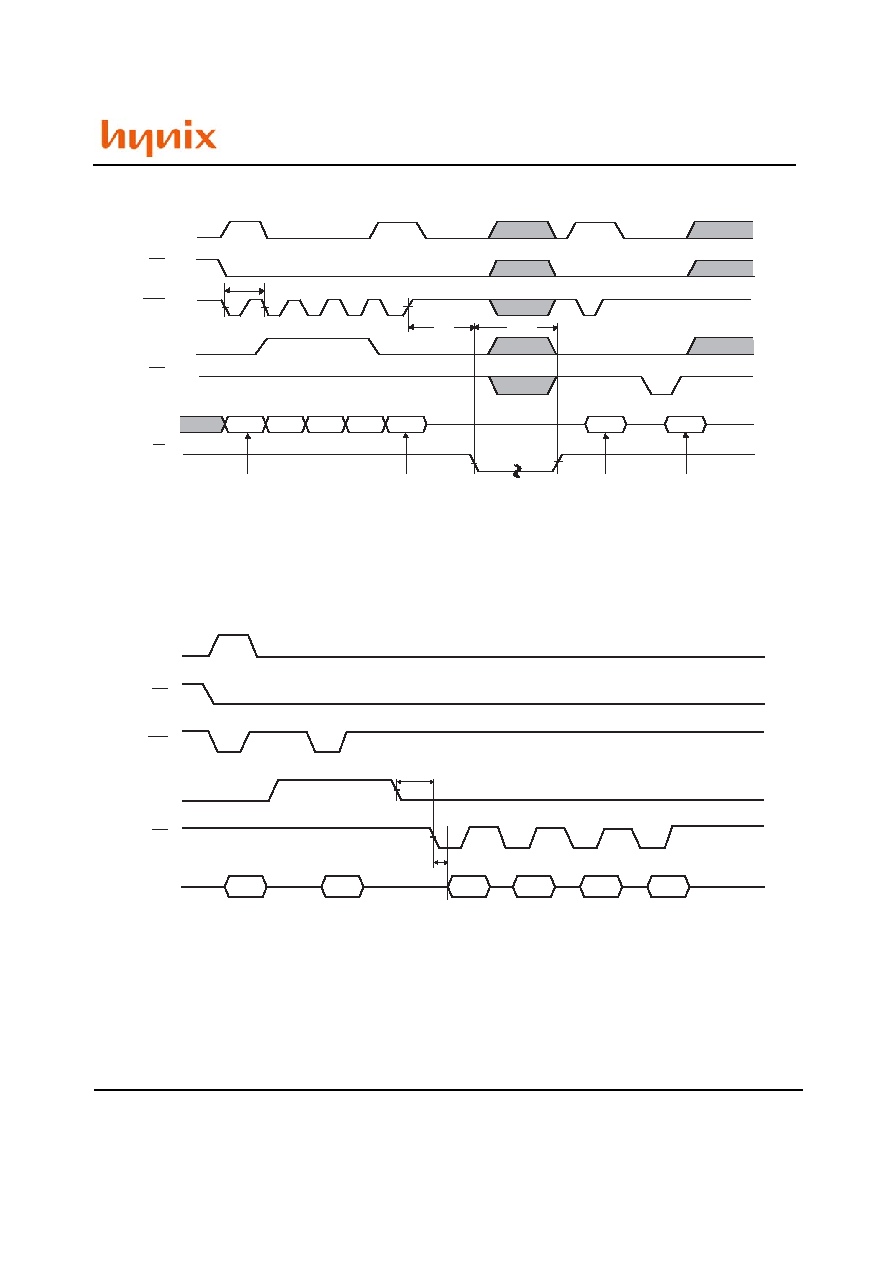
Figure 5: Command Latch Cycle
Table 18: Lock Status Code

Rev. 0.5 / Jul. 2006
29
HY27UF084G2M Series
4Gbit (512Mx8bit) NAND Flash
Figure 6: Address Latch Cycle
Figure 7. Input Data Latch Cycle

Rev. 0.5 / Jul. 2006
30
HY27UF084G2M Series
4Gbit (512Mx8bit) NAND Flash
Figure 8: Sequential Out Cycle after Read (CLE=L, WE=H, ALE=L)
Figure 9: Sequential Out Cycle after Read (EDO Type CLE=L, WE=H, ALE=L)

Rev. 0.5 / Jul. 2006
31
HY27UF084G2M Series
4Gbit (512Mx8bit) NAND Flash
Figure 10: Status Read Cycle
Figure 11: Read1 Operation (Read One Page)

Rev. 0.5 / Jul. 2006
32
HY27UF084G2M Series
4Gbit (512Mx8bit) NAND Flash
Figure 12: Read1 Operation intercepted by CE
Rev. 0.5 / Jul. 2006
33
HY27UF084G2M Series
4Gbit (512Mx8bit) NAND Flash
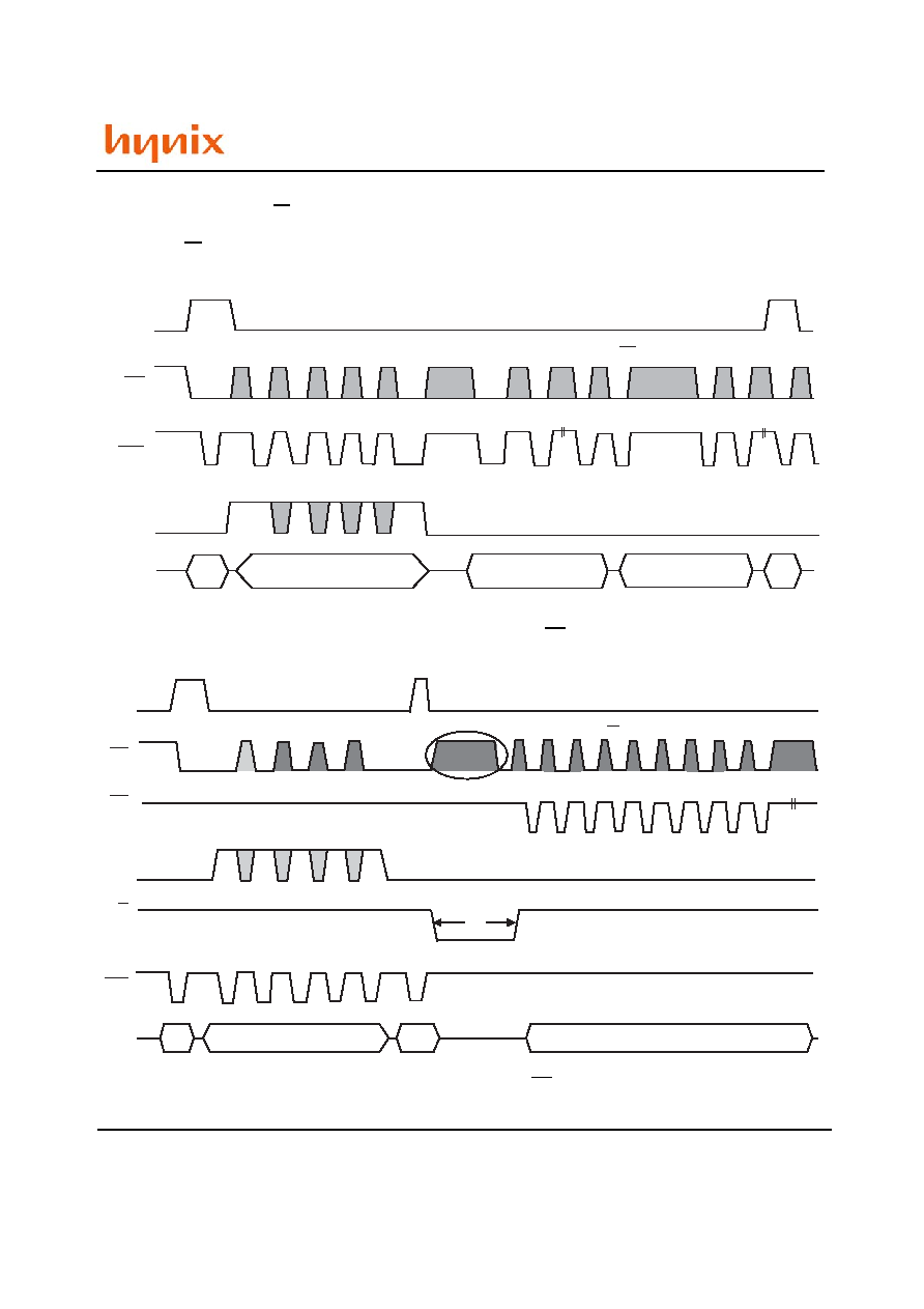
Figure 13 : Random Data output

Rev. 0.5 / Jul. 2006
34
HY27UF084G2M Series
4Gbit (512Mx8bit) NAND Flash
Figure 14: Page Program Operation

Rev. 0.5 / Jul. 2006
35
HY27UF084G2M Series
4Gbit (512Mx8bit) NAND Flash
Figure 15 : Random Data In
Rev. 0.5 / Jul. 2006
36
HY27UF084G2M Series
4Gbit (512Mx8bit) NAND Flash
Figure 16 : Copy Back Program

Rev. 0.5 / Jul. 2006
37
HY27UF084G2M Series
4Gbit (512Mx8bit) NAND Flash
Figure 17 : Cache Program

Rev. 0.5 / Jul. 2006
38
HY27UF084G2M Series
4Gbit (512Mx8bit) NAND Flash
Figure 18 :Cache Read RE high
Rev. 0.5 / Jul. 2006
39
HY27UF084G2M Series
4Gbit (512Mx8bit) NAND Flash
Figure 19: Block Erase Operation (Erase One Block)
Figure 20: Read ID Operation

Rev. 0.5 / Jul. 2006
40
HY27UF084G2M Series
4Gbit (512Mx8bit) NAND Flash
Figure 21: start address at page start :after 1st latency uninterrupted data flow
Figure 22: exit from cache read in 5us when device internally is reading
Rev. 0.5 / Jul. 2006
41
HY27UF084G2M Series
4Gbit (512Mx8bit) NAND Flash
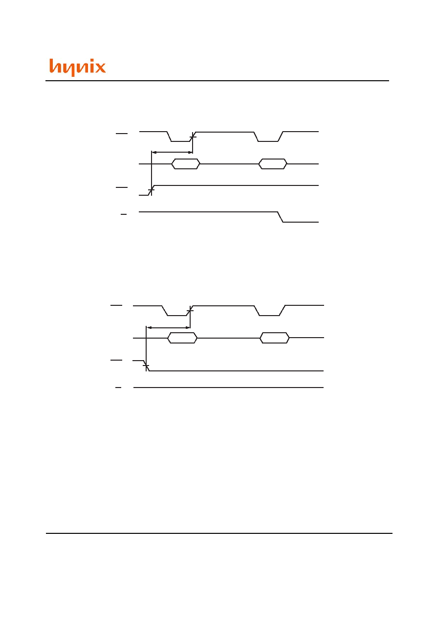
System Interface Using CE don't care
To simplify system interface, CE may be deasserted during data loading or sequential data-reading as shown below.
So, it is possible to connect NAND Flash to a microporcessor. The only function that was removed from standard NAND
Flash to make CE don't care read operation was disabling of the automatic sequential read function.
Figure 23: Program Operation with CE don't-care.
Figure 24: Read Operation with CE don't-care.
Rev. 0.5 / Jul. 2006
42
HY27UF084G2M Series
4Gbit (512Mx8bit) NAND Flash
Figure 25: Lock Command
Figure 26: Unlock Command Sequence

Rev. 0.5 / Jul. 2006
43
HY27UF084G2M Series
4Gbit (512Mx8bit) NAND Flash
Figure 27: Lock Tight Command
Figure 28: Lock Status Read Timing

Rev. 0.5 / Jul. 2006
44
HY27UF084G2M Series
4Gbit (512Mx8bit) NAND Flash
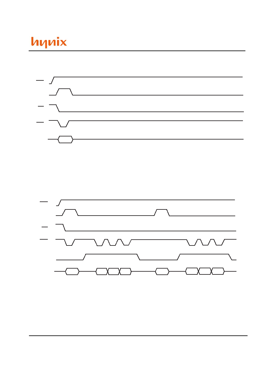
Figure 30: Reset Operation
Figure 29: Automatic Read at Power On

Rev. 0.5 / Jul. 2006
45
HY27UF084G2M Series
4Gbit (512Mx8bit) NAND Flash
Figure 31: Power On and Data Protection Timing
VTH = 2.5 Volt for 3.3 Volt Supply devices
Rev. 0.5 / Jul. 2006
46
HY27UF084G2M Series
4Gbit (512Mx8bit) NAND Flash
Figure 32: Ready/Busy Pin electrical specifications

Rev. 0.5 / Jul. 2006
47
HY27UF084G2M Series
4Gbit (512Mx8bit) NAND Flash
Figure 33: Lock/Unlock FSM Flow Cart
Figure 34 : page programming within a block

Rev. 0.5 / Jul. 2006
48
HY27UF084G2M Series
4Gbit (512Mx8bit) NAND Flash
Bad Block Management
Devices with Bad Blocks have the same quality level and the same AC and DC characteristics as devices where all the
blocks are valid. A Bad Block does not affect the performance of valid blocks because it is isolated from the bit line and
common source line by a select transistor.
The devices are supplied with all the locations inside valid blocks erased(FFh). The Bad Block Information is written
prior to shipping. Any block where the
1st Byte
in the spare area of the 1st or 2nd page(if the 1st page is Bad) does
not contain FFh is a Bad Block. The Bad Block Information must be read before any erase is attempted as the Bad
Block Information may be erased. For the system to be able to recognize the Bad Blocks based on the original informa-
tion it is recommended to create a Bad Block table following the flowchart shown in Figure 35. The 1st block, which is
placed on 00h block address is guaranteed to be a valid block.
Bad Replacement
Over the lifetime of the device additional Bad Blocks may develop. In this case the block has to be replaced by copying
the data to a valid block. These additional Bad Blocks can be identified as attempts to program or erase them will give
errors in the Status Register.
As the failure of a page program operation does not affect the data in other pages in the same block, the block can be
replaced by re-programming the current data and copying the rest of the replaced block to an available valid block.
The Copy Back Program command can be used to copy the data to a valid block.
See the "Copy Back Program" section for more details.
Refer to Table 19 for the recommended procedure to follow if an error occurs during an operation.
Operation
Recommended Procedure
Erase
Block Replacement
Program
Block Replacement or ECC (with 1bit/512byte)
Read
ECC (with 1bit/512byte)
Table 19: Block Failure
Figure 35: Bad Block Management Flowchart

Rev. 0.5 / Jul. 2006
49
HY27UF084G2M Series
4Gbit (512Mx8bit) NAND Flash
Write Protect Operation
The Erase and Program Operations are automatically reset when WP goes Low (tWW = 100ns, min). The operations
are enabled and disabled as follows (Figure 36~39)
Figure 36: Enable Programming
Figure 37: Disable Programming
Rev. 0.5 / Jul. 2006
50
HY27UF084G2M Series
4Gbit (512Mx8bit) NAND Flash
Figure 38: Enable Erasing
Figure 39: Disable Erasing

Rev. 0.5 / Jul. 2006
51
HY27UF084G2M Series
4Gbit (512Mx8bit) NAND Flash
5. APPENDIX : Extra Features
5.1 Automatic Page0 Read after Power Up
The timing diagram related to this operation is shown in Fig. 29
Due to this functionality the CPU can directly download the boot loader from the first page of the NAND flash, storing
it inside the internal cache and starting the execution after the download completed.
5.2 Addressing for program operation
Within a block, the pages must be programmed consecutively from LSB (least significant bit) page of the block to MSB
(most significant bit) page of the block. Random address programming is prohibited. See Fig. 34.

Rev. 0.5 / Jul. 2006
52
HY27UF084G2M Series
4Gbit (512Mx8bit) NAND Flash
Table 20: 48-TSOP1 - 48-lead Plastic Thin Small Outline,
12 x 20mm, Package Mechanical Data
Symbol
millimeters
Min
Typ
Max
A
1.200
A1
0.050
0.150
A2
0.980
1.030
B
0.170
0.250
C
0.100
0.200
CP
0.100
D
11.910
12.000
12.120
E
19.900
20.000
20.100
E1
18.300
18.400
18.500
e
0.500
L
0.500
0.680
alpha
0
5
Figure 40. 48-TSOP1 - 48-lead Plastic Thin Small Outline, 12 x 20mm, Package Outline

Rev. 0.5 / Jul. 2006
53
HY27UF084G2M Series
4Gbit (512Mx8bit) NAND Flash
Symbol
millimeters
Min
Typ
Max
A
16.90
17.00
17.10
A1
13.00
A2
12.00
B
11.90
12.00
12.10
B1
10.00
B2
6.00
C
1.00
C1
1.50
C2
2.00
D
1.00
D1
1.00
E
0.55
0.60
0.65
CP1
0.65
0.70
0.75
CP2
0.95
1.00
1.05
Table 21: 52-ULGA, 12 x 17mm, Package Mechanical Data
Figure 41. 52-ULGA, 12 x 17mm, Package Outline
(Top view through package)

Rev. 0.5 / Jul. 2006
54
HY27UF084G2M Series
4Gbit (512Mx8bit) NAND Flash
MARKING INFORMATION-
TSOP1/ULGA
P ackage
M arking Exam ple
TS O P 1
/
U LG A
K
O
R
H
Y
2
7
U
F
0
8
4
G
2
M
x
x
x
x
Y
W
W
x
x
- hynix
- K O R
- H Y 27 U F084 G 2M xxxx
H Y : H ynix
2 7: N AN D Flash
U : Pow er Supply
F: Classification
0 8: Bit O rganization
4 G : D ensity
2 : M ode
M : Version
x: Package Type
x: Package M aterial
x: O perating Tem perature
x: Bad Block
- Y : Year (ex: 5= year 2005, 06= year 2006)
- w w : W ork W eek (ex: 12= w ork w eek 12)
- xx: Process Code
N ote
- C apital Letter
- Sm all Letter
: H ynix Sym bol
: O rigin Country
: U (2.7V~ 3.6V)
: Single Level Cell
: 08(x8)
: 4G bit
: 2(1nCE & 1R/nB; Sequential R ow Read D isable)
: 1st G eneration
: T(48-TSO P1), U (52-U LG A)
: Blank(N orm al), P(Lead Free)
: C(0 ~ 70 ), E(-25 ~ 85 )
M (-30 ~ 85 ), I(-40 ~ 85 )
: B(Included Bad Block), S(1~ 5 Bad Block),
P(All G ood Block)
: Fixed Item
: N on-fixed Item
: Part N um ber