Äîêóìåíòàöèÿ è îïèñàíèÿ www.docs.chipfind.ru

HV7151SP
CMOS Image Sensor
Confidential
With Image Signal Processing
This document is a general product description and is subject to change without notice. Hynix
Semiconductor Inc. does not assume any responsibility for use of circuits described and no patent
licenses are implied.
- 1 -
2003 Hynix Semiconductor Inc.
CMOS Image Sensor
with
Image Signal Processing
HV7151SP
Hynix Semiconductor Inc.
Preliminary Release
Version 0.7
HV7151SP
CMOS Image Sensor
Confidential
With Image Signal Processing
This document is a general product description and is subject to change without notice. Hynix
Semiconductor Inc. does not assume any responsibility for use of circuits described and no patent
licenses are implied.
- 2 -
2003 Hynix Semiconductor Inc.
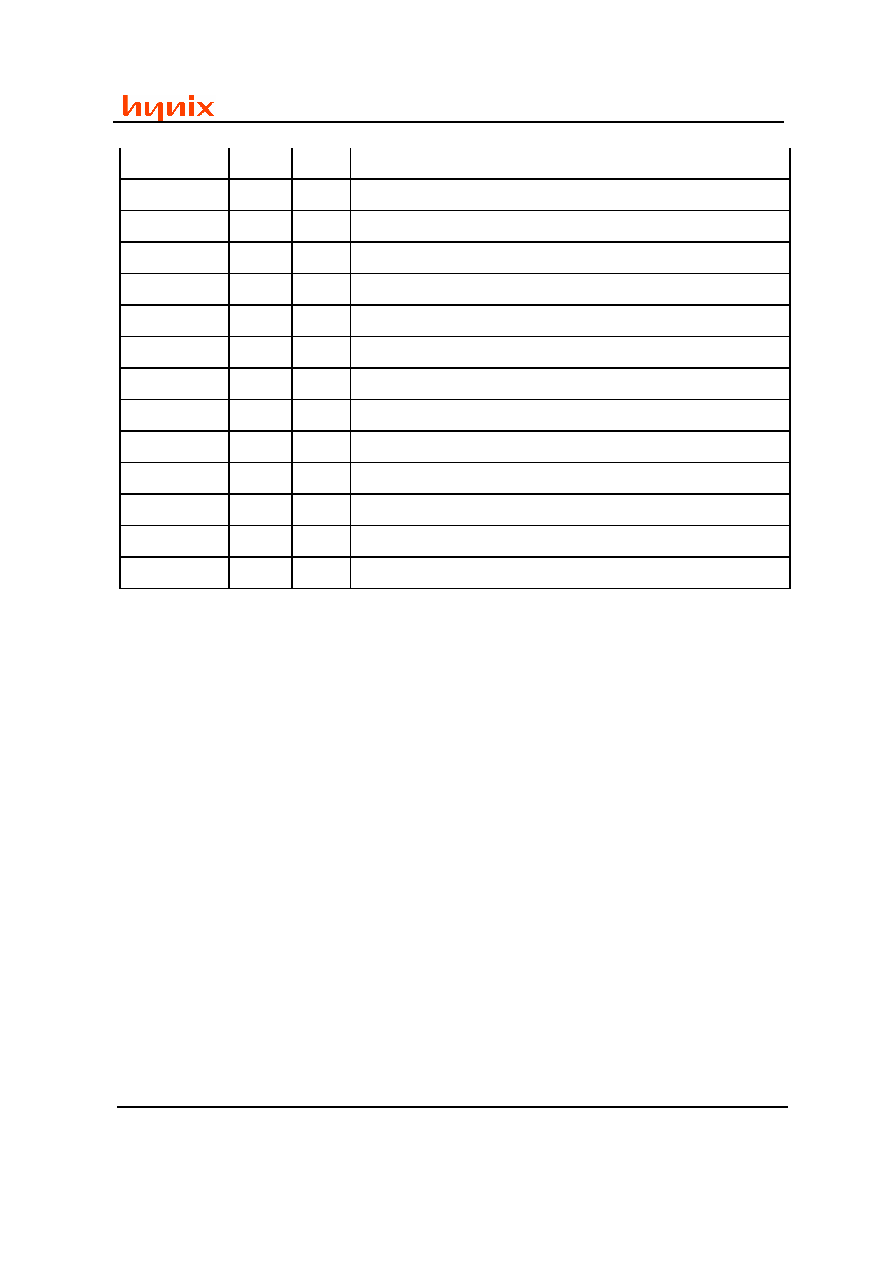
Revision History
Revision
Script Date
Comments
0.0
2003-June
HV7151SP Preliminary is released
0.1
2003-June
HV7151SP version 0.1 is released
0.2
2003-July
HV7151SP version 0.2 is released
0.5
2003-August
HV7151SP version 0.5 is released
0.6
2003-November
Frame rate Calculation is added
0.7
2004-January
ENB Setting Guide Information and
Recommend Circuit Information is Added
Copyright by Hynix Semiconductor Inc., all right reserved 2003

HV7151SP
CMOS Image Sensor
Confidential
With Image Signal Processing
This document is a general product description and is subject to change without notice. Hynix
Semiconductor Inc. does not assume any responsibility for use of circuits described and no patent
licenses are implied.
- 3 -
2003 Hynix Semiconductor Inc.
Contents
General Description ....................................................................................................................5
Features ....................................................................................................................................5
Block Diagram ...........................................................................................................................6
Pixel Structure ...........................................................................................................................7
Pin Diagram...............................................................................................................................8
Pin Diagram...............................................................................................................................9
Functional Description ..............................................................................................................10
Pixel Architecture ..............................................................................................................10
Sensor Imaging Operation ..................................................................................................10
On-chip Frequency Synthesizer ..........................................................................................11
11bit on-chip ADC..............................................................................................................11
Gamma Correction.............................................................................................................11
Color Interpolation..............................................................................................................12
Sub-sampling Mode ...........................................................................................................12
Scaling Mode ....................................................................................................................12
Color Correction.................................................................................................................12
Color Space Conversion & Reverse Color Space Conversion ..................................................13
Luminance Processing Contrast, Brightness adjustment ....................................................14
Chrominance Processing Saturation adjustment ................................................................14
Edge Enhancement ...........................................................................................................14
Chroma Suppression..........................................................................................................14
Automatic Flicker Cancellation............................................................................................14
Output Formatting..............................................................................................................15
Auto Exposure Control .......................................................................................................15
Auto White Balance...........................................................................................................15
Register Description .................................................................................................................16
Anti-Banding Configuration ........................................................................................................60
Frame Timing...........................................................................................................................60
Output Data according to Video Mode ........................................................................................66
Bayer Data Format ...................................................................................................................79
I2C Chip Interface.....................................................................................................................80
AC/DC Characteristics..............................................................................................................82
Electro-Optical Characteristics ..................................................................................................85

HV7151SP
CMOS Image Sensor
Confidential
With Image Signal Processing
This document is a general product description and is subject to change without notice. Hynix
Semiconductor Inc. does not assume any responsibility for use of circuits described and no patent
licenses are implied.
- 4 -
2003 Hynix Semiconductor Inc.
Package information .................................................................................................................86
Reference Circuit Information .....................................................................................................88
MEMO ....................................................................................................................................89

HV7151SP
CMOS Image Sensor
Confidential
With Image Signal Processing
This document is a general product description and is subject to change without notice. Hynix
Semiconductor Inc. does not assume any responsibility for use of circuits described and no patent
licenses are implied.
- 5 -
2003 Hynix Semiconductor Inc.
General Description
HV7151SP is a highly integrated single chip CMOS color image sensor implemented by proprietary
Hynix 0.18um CMOS sensor process realizing high sensitivity and wide dynamic range. Active pixel
array is 1164x886. Each active pixel composed of 4 transistors, it has a micro-lens to enhance
sensitivity, and converts photon energy to analog pixel voltage. On-chip 11bit Analog to Digital
Converter (ADC) digitizes analog pixel voltage, and on-chip Correlated Double Sampling (CDS)
scheme reduces Fixed Pattern Noise (FPN) dramatically. General image processing functions are
implemented to diversify its applications, and various output formats are supported for the sensor to
easily interface with different video codec chips. The integration of sensor function and image
processing functions make HV7151SP especially very suitable for mobile imaging systems such as
digital still camera, PC input camera and IMT-2000 phone's video part that requires very low power
and system compactness.
Features
n
Optical Format : 1/4 inch / Pixel Size : 3.2
µ
m x 3.2
µ
m
n
Active Pixel Array : 1170 x 886
n
Multiple Video Modes : 1152x864(MEGA), 640x480(VGA), 576x432(1/4 MEGA), 352x288(CIF),
320x240(QVGA), 288x216(1/16 MEGA), 176x144(QCIF)
n
Bayer RGB Color filter array / Micro-lens for high sensitivity
n
On-chip Frequency Synthesizer
n
On-chip 11 bit Analog to Digital Converter
n
Correlated Double Sampling (CDS) for reduction of Fixed Pattern Noise (FPN)
n
Automatic Flicker Cancellation (AFC)
n
Automatic Black Level Calibration (ABLC)
n
Gamma Correction by programmable piecewise linear approximation
n
5x5 Color Interpolation
n
Color Correction by programmable 3x3 matrix operation
n
Color Space Conversion from RGB to YCbCr and Reverse Conversion from YCbCr to RGB
n
Image adjustment :Contrast, Brightness, Saturation, Edge Enhancement, Chroma Suppression
n
Various Output Formats: CCIR-601, CCIR-656 Compatible
YCbCr 4:2:2, YCbCr 4:4:4, RGB 4:4:4, RGB 565, Bayer
n
8bit/16bit Data Bus Mode
n
Automatic Exposure Control and Automatic White Balance Control
n
Power Save Mode
HV7151SP
CMOS Image Sensor
Confidential
With Image Signal Processing
This document is a general product description and is subject to change without notice. Hynix
Semiconductor Inc. does not assume any responsibility for use of circuits described and no patent
licenses are implied.
- 6 -
2003 Hynix Semiconductor Inc.
n
Typical Supply Voltage: Internal 1.8V and I/O 2.5V
n
Operation Temperature : -10 ~ +50 degrees Celsius
n
Package Types: CLCC 40 PIN, COB(Chip-on-Board), COF(Chip-on-Flex)
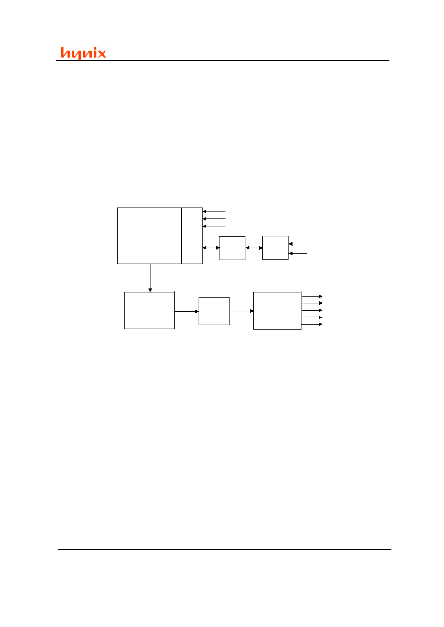
Block Diagram
Analog
Signal
Processing
Digital
Signal
Processing
Pixel Array
1170x886
Timing
Control
Config
Registers
I2C
Slave
11bit ADC
RESETB
MCLK
ENB
SCK
SDA
VCLK
VSYNC
HSYNC
Y[7:0]
C[7:0]
HV7151SP
CMOS Image Sensor
Confidential
With Image Signal Processing
This document is a general product description and is subject to change without notice. Hynix
Semiconductor Inc. does not assume any responsibility for use of circuits described and no patent
licenses are implied.
- 7 -
2003 Hynix Semiconductor Inc.
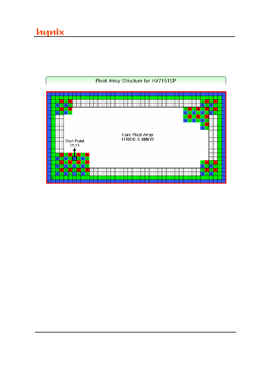
Pixel Structure
HV7151SP
CMOS Image Sensor
Confidential
With Image Signal Processing
This document is a general product description and is subject to change without notice. Hynix
Semiconductor Inc. does not assume any responsibility for use of circuits described and no patent
licenses are implied.
- 8 -
2003 Hynix Semiconductor Inc.
Pin Diagram
16 17 18 19 20 21 22 23 24 25
5 4 3 2 1
35
34
33
32
31
30
29
28
27
26
6
7
8
9
10
11
12
13
14
15
HV7151SP
CLCC 40 PIN
Top View
DVDDC
DGNDC
C[7]
C[6]
C[5]
C[4]
C[3]
C[2]
C[1]
C[0]
Y[7]
Y[6]
Y[5]
Y[4]
Y[3]
Y[2]
Y[1]
Y[0]
DGNDI
DVDDI
DGNDI
DVDDIH
MCLK
VCLK
HSYNC
VSYNC
AINP
AINN
AVDD
AGND
AVDDH
DVDDI
DGNDI
ENB
RESETB
STROBE
SCK
SDA
DGNDIH
DVDDIH
40 39 38 37 36
HV7151SP
CMOS Image Sensor
Confidential
With Image Signal Processing
This document is a general product description and is subject to change without notice. Hynix
Semiconductor Inc. does not assume any responsibility for use of circuits described and no patent
licenses are implied.
- 9 -
2003 Hynix Semiconductor Inc.
Pin Diagram
C[7:0] should be set up as pull-up or pull-down when 8bit output mode is used.
Pin
Type
Symbol
Description
36-40, 1-3
B
Y[7:0]
Video Luminance Data[7:0]
4
G
DGNDI
Digital Ground for I/O Driver
5
P
DVDDI
1.8V Digital Power for I/O Driver
6
P
DVDDC
1.8V Power for Internal Digital Block
7
G
DGNDC
Ground for Internal Digital Block
8-15
B
C[7:0]
Video Chrominance Data[7:0]
16
PH
DVDDIH
2.5V Digital Power for I/O Driver
17
G
DGNDIH Digital Ground for I/O Driver
18
B
SDA
I2C Standard data I/O port
19
I
SCK
I2C Clock Input
20
O
STROBE Strobe Signal Output
21
I
RESETB Sensor Reset, Low Active
22
I
ENB
Sensor sleep mode is controlled externally by this pin when
sleep mode register bit is low.
ENB low : sleep mode, ENB high : normal mode
23
G
DGNDI
Digital Ground for I/O Driver
24
P
DVDDI
1.8V Digital Power for I/O Driver
25
PH
AVDDPH 2.5V Analog Power for Pixel Block
26
G
AGND
Analog Ground for Analog Block
27
P
AVDD
1.8V Power for Internal Analog Block
28
AI
AINN
Analog Input Minus for Test ADC
29
AI
AINP
Analog Input Plus for Test ADC
30
B
VSYNC
Video Frame Synchronization signal. VSYNC is active at start
of image data frame.
31
B
HSYNC
Video Horizontal Line Synchronization signal. Image data is
valid, when HSYNC is high.
32
B
VCLK
Video Output Clock
33
I
MCLK
Master Input Clock
34
PH
DVDDIH
2.5V Digital Power for I/O Driver
35
G
DGNDI
Digital Ground for I/O Driver
HV7151SP
CMOS Image Sensor
Confidential
With Image Signal Processing
This document is a general product description and is subject to change without notice. Hynix
Semiconductor Inc. does not assume any responsibility for use of circuits described and no patent
licenses are implied.
- 10 -
2003 Hynix Semiconductor Inc.
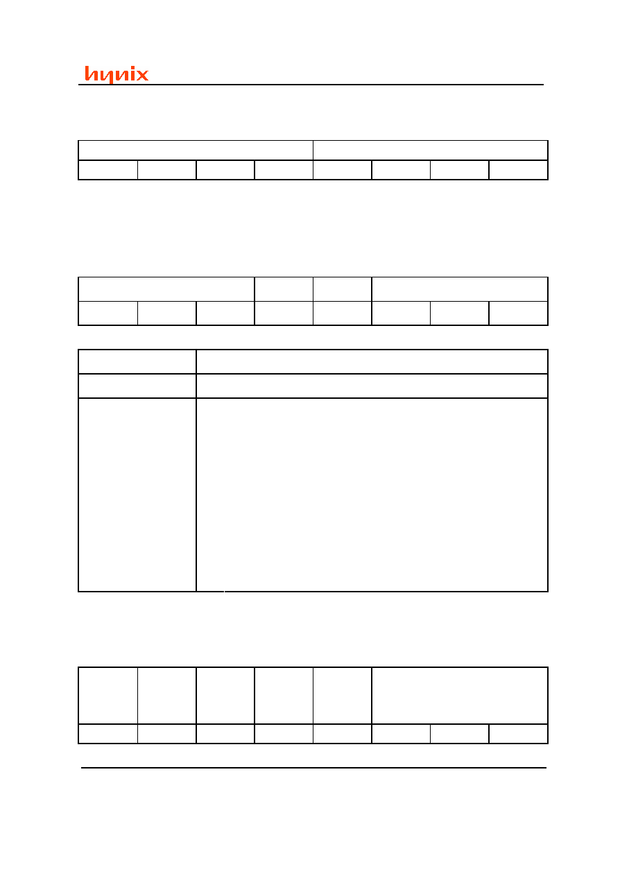
Functional Description
Pixel Architecture
Pixel architecture is a 4 transistor NMOS pixel design. The additional use of a dedicated transfer
transistor in the architecture reduces most of reset level noise so that fixed pattern noise is not visible.
Furthermore, micro-lens is placed upon each pixel in order to increase fill factor so that high pixel
sensitivity is achieved.
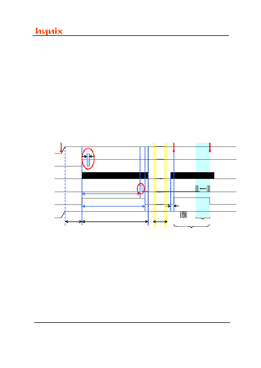
ENB Setting guide information for normal stand-by mode
It is necessary that this kind of initialization sequence for the normal stand-by mode of HV7151SP
after system power on
ex) If MCLK = 19.2[Mhz] and PLL 2x,
=> 2.68[Mcycle] / 38.4[MHz] = 69.79 ms
The time period of ENB high value have to keep for 69.79[ms] or more
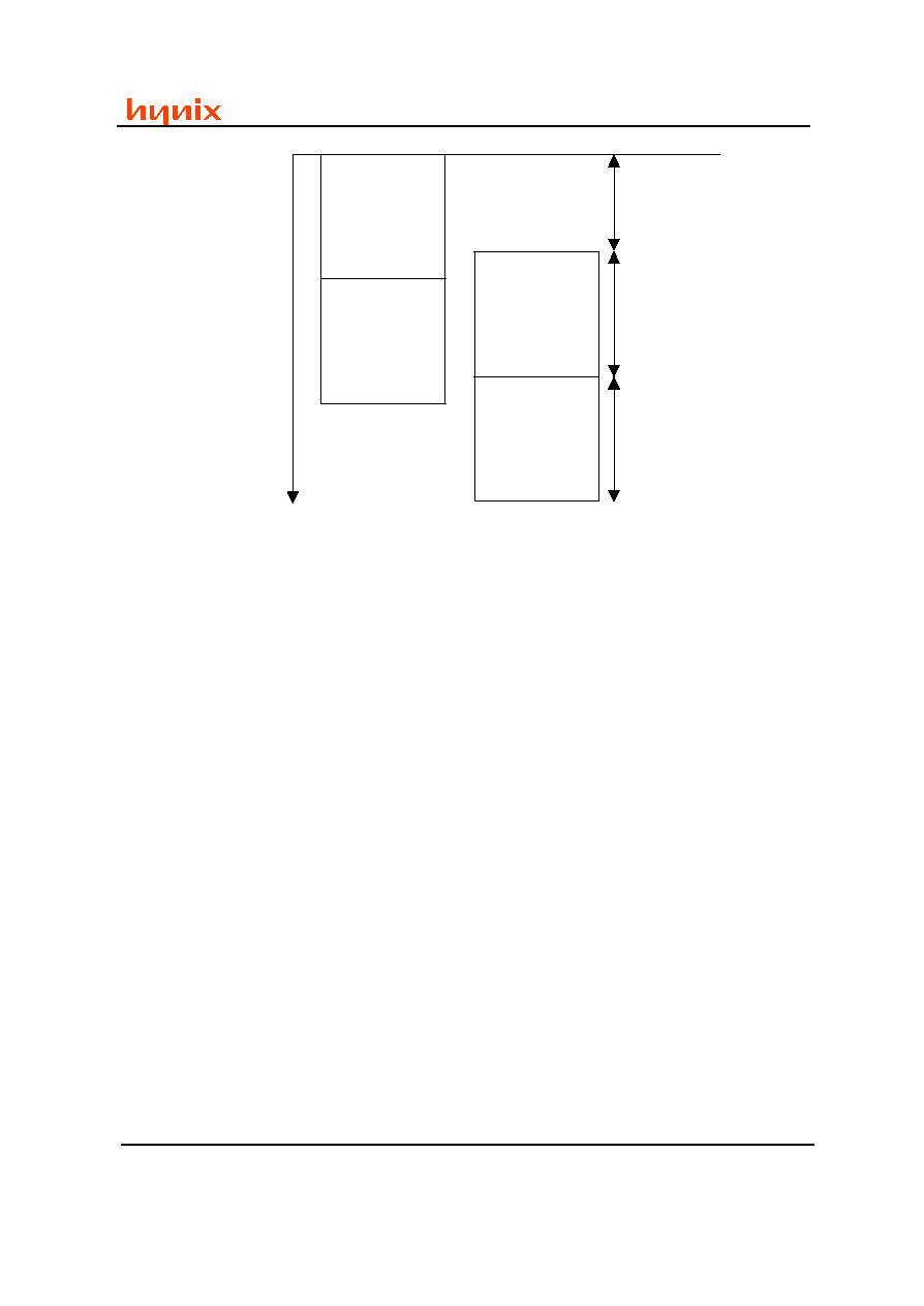
Sensor Imaging Operation
Imaging operation is implemented by the offset mechanism of integration domain and scan
domain(rolling shutter scheme). First integration plane is initiated, and after the programmed
integration time is elapsed, scan plane is initiated, then image data start being produced.
DVDD/AVDD
RESETB
MCLK
VSYNC
I2C
ENB
Don
'
t care
Low
Low
Low
Low
System power On
Initialization sequence
2.68 [
Mcycle
] for logic stable time
2.56 [
Mcycle
] for 1'st VSYNC out
More than 4cycle
Don
'
t care
1ms
Sensor operation sequence
Sensor Power down sequence
Camera Mode
Video stream
1
'
st VSYNC out
DVDD/AVDD
RESETB
MCLK
VSYNC
I2C
ENB
Don
'
t care
Low
Low
Low
Low
System power On
Initialization sequence
More than 4cycle
Don
'
t care
1ms
Sensor operation sequence
Sensor Power down sequence
Camera Mode
Video stream
1
'
st VSYNC out
HV7151SP
CMOS Image Sensor
Confidential
With Image Signal Processing
This document is a general product description and is subject to change without notice. Hynix
Semiconductor Inc. does not assume any responsibility for use of circuits described and no patent
licenses are implied.
- 11 -
2003 Hynix Semiconductor Inc.
Integration
Time
Frame 0
Time
Time
Integration
Plane
Frame 0
Integration
Plane
Frame 1
Scan
Plane
Frame 0
Scan
Plane
Frame 1
Frame 1
Time
On-chip Frequency Synthesizer
On-chip Frequency Synthesizer generates variable frequency according to the proportion of
Reference(PREFDIV) to Feedback(PFDDIV) Divisor. Operating frequency is fully programmable and
output range is 5MHz to 100MHz.
11bit on-chip ADC
On-chip ADC converts analog pixel voltage to 11bit digital data.
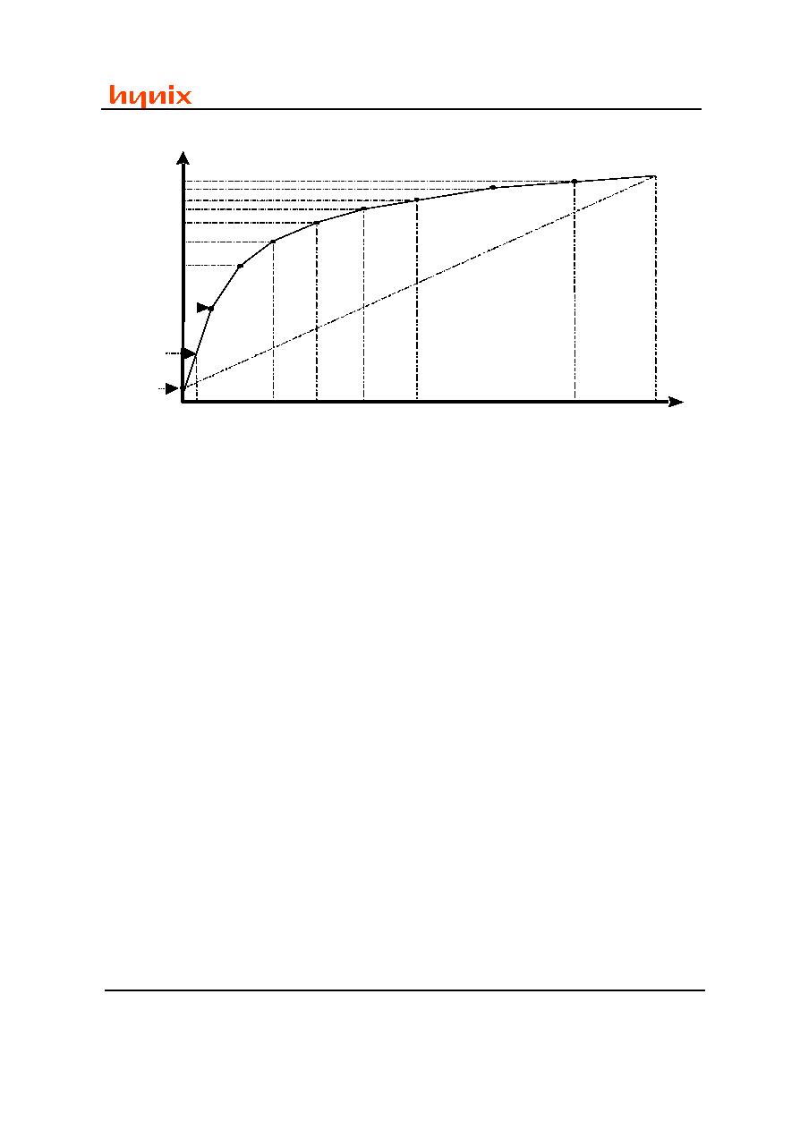
Gamma Correction
Piecewise linear approximation method is implemented. Ten piece linear segments are supported and
user-programmable.
HV7151SP
CMOS Image Sensor
Confidential
With Image Signal Processing
This document is a general product description and is subject to change without notice. Hynix
Semiconductor Inc. does not assume any responsibility for use of circuits described and no patent
licenses are implied.
- 12 -
2003 Hynix Semiconductor Inc.
Gamma Transfer Function
In
Out
Start 0
Start 1
0
128
256
384
512
1024
1536
3 2 64
Start 2
2047
Start 9
:
:
8
Color Interpolation
5x5 linear color interpolation is used to interpolate missing R, G, or B for mosaic image data from
pixel array. Interpolation is done by moving 5x5 interpolation window by one pixel horizontally and
vertically.
Sub-sampling Mode
The sub-sampling modes such as 1/4 sub-sampling and 1/16 sub-sampling are supported. The sub-
sampling sequence is as below. For example 1/4 sub-sampling, Row data are picked out from R,G,B
bayer raw data by the rate of four to two. And after 5x5 linear color interpolation, column data also are
picked out the rate of two to one. 1/16 sub-sampling is similar to 1/4 sub-sampling.
Scaling Mode
In addition to the sub-sampling mode, HV7151SP supports the scaling modes, such as 5/9 scaling
VGA, 5/18 scaling QVGA, 1/3 scaling CIF and 1/6 QCIF. Because HV7151SP normal image
size(1152x864) is not a multiple proportion of VGA/QVGA or CIF/QCIF image size, output data and
output clock of scaling mode are asymmetry.
Color Correction
Generally, the color spread effect is mainly caused by color filter characteristics. The effect is
compensated by 3x3 color correction operation. Color correction matrix may be resolved by
measuring sensor's color spread characteristics for primary color source and calculating the inverse

HV7151SP
CMOS Image Sensor
Confidential
With Image Signal Processing
This document is a general product description and is subject to change without notice. Hynix
Semiconductor Inc. does not assume any responsibility for use of circuits described and no patent
licenses are implied.
- 13 -
2003 Hynix Semiconductor Inc.
matrix of color spread matrix. Nine registers for matrix coefficients are used in color correction
operation to get the optimal pure color. The relationship between input color and color-corrected color
is defined as below formula.
·
=
B
G
R
CRCM
CRCM
CRCM
CRCM
CRCM
CRCM
CRCM
CRCM
CRCM
B
G
R
33
32
31
23
22
21
13
12
11
where
R,G,B = Sensor color output
R',G',B' = Color-corrected output
Coefficients CRCMxx are programmable from 127/64 ~ 127/64. Programming register value for
intended color correction matrix coefficients should be resolved by the following equations.
For positive values, CRCMxx = Integer(Real Coefficient Value x 64);
For negative values, CRCMxx = Two's Complement(Integer(Real Coefficient Value x 64));
Real Coefficient Value values from 127/64 ~ 127/64 can be programmed.
Color Space Conversion & Reverse Color Space Conversion
Both of color space conversion and reverse color space conversion are implemented by 3x3 matrix
operation. Output ranges of color space conversion and reverse conversion are existed two modes.
One is 16
Y
235, 16
Cb,Cr
240 & 16
reverse-R,G,B
235 and Another is 0
Y,Cb,Cr
255 & 0
reverse-R,G,B
255. These different modes are selected by control register.
For color space conversion and reverse conversion matrix, the equation from CCIR-601 standard is
normally used.
< Conversion Equation >
Mode 1 :
255
~
0
:
255
~
0
:
255
~
0
:
128
128
0
081
.
0
419
.
0
500
.
0
500
.
0
331
.
0
169
.
0
114
.
0
587
.
0
299
.
0
Range
Range
Range
B
G
R
Cr
Cb
Y
+
·
-
-
-
-
=
Mode 2 :
240
~
16
:
240
~
16
:
235
~
16
:
128
128
16
071
.
0
368
.
0
439
.
0
439
.
0
291
.
0
148
.
0
098
.
0
504
.
0
257
.
0
Range
Range
Range
B
G
R
Cr
Cb
Y
+
·
-
-
-
-
=

HV7151SP
CMOS Image Sensor
Confidential
With Image Signal Processing
This document is a general product description and is subject to change without notice. Hynix
Semiconductor Inc. does not assume any responsibility for use of circuits described and no patent
licenses are implied.
- 14 -
2003 Hynix Semiconductor Inc.
In the above equations, R, G, and B are gamma-corrected values.
< Reverse Conversion Equation >
235
~
16
255
~
0
:
235
~
16
255
~
0
:
235
~
16
255
~
0
:
128
128
772
.
1
1
0
344
.
0
1
714
.
0
0
1
402
.
1
or
Range
or
Range
or
Range
Cb
Y
Cr
B
G
R
-
-
·
-
-
=
Same matrix equations are applied to mode1 and mode2 in the reverse color space conversion. And
previously, output ranges 0 ~ 255 or 16 ~ 235 are decided by input ranges of Y,Cb,Cr.
Luminance Processing Contrast, Brightness adjustment
For contrast adjustment, Y digital channels are scaled by the contrast factor. Contrast factor
resolution is 1/128 and its range is 0 ~ 255/128.
For brightness adjustment, there is added a brightness factor to Y digital channels. Brightness factor
range is 128 ~ 127 and register value for brightness adjustment is following below.
For positive values, Brightness factor = Integer;
For negative values, Brightness factor = Two's Complement(Integer);
For example, if brightness factor is 3, register value is 8'h03 and if brightness factor is -3, register
value is 8'hfd.
Chrominance Processing Saturation adjustment
For saturation adjustment, Cb,Cr digital Channels are scaled by the saturation factor. Saturation
factor resolution is 1/128 and its range is 0 ~ 255/128.
Edge Enhancement
Edge enhancement is performed for increasing sharpness of image. Edge weight factor is user-
programmable and its range is 0.3 ~ 1.0.
Chroma Suppression
Chroma suppression is performed in the dark environment for suppressing the color and decreasing
dark bad pixel effect. Suppression level is varied in accordance with amplifier gain and saturation level
is user-programmable.
Automatic Flicker Cancellation
Banding noise, caused by difference between frequency of light sources and frequency of integration
time of pixel, is always generated in CMOS image sensor. For Automatic Flicker Cancellation,
integration time is adjusted automatically in accordance with frequency of light sources.

HV7151SP
CMOS Image Sensor
Confidential
With Image Signal Processing
This document is a general product description and is subject to change without notice. Hynix
Semiconductor Inc. does not assume any responsibility for use of circuits described and no patent
licenses are implied.
- 15 -
2003 Hynix Semiconductor Inc.
Output Formatting
The output formats such as YCbCr 4:2:2, YCbCr 4:4:4, RGB 4:4:4, RGB 5:6:5 and Bayer Raw Data
are supported. Possible output bus widths are 8 bits and 16bits, and the sequence of Cb and Cr or R
and B are programmable. The output formats are compatible with Recommendation CCIR-601, CCIR-
656.
Auto Exposure Control
Y mean value is continuously calculated every frame, and the integration time or amp gain value are
increased or decreased according to difference between target Y mean value and current frame Y
mean value.
Auto White Balance
Cb/Cr frame mean value is calculated every frame and according to Cb/Cr frame mean values'
displacement from Cb/Cr white target point, R/B scaling values for R/B data are resolved.
HV7151SP
CMOS Image Sensor
Confidential
With Image Signal Processing
This document is a general product description and is subject to change without notice. Hynix
Semiconductor Inc. does not assume any responsibility for use of circuits described and no patent
licenses are implied.
- 16 -
2003 Hynix Semiconductor Inc.
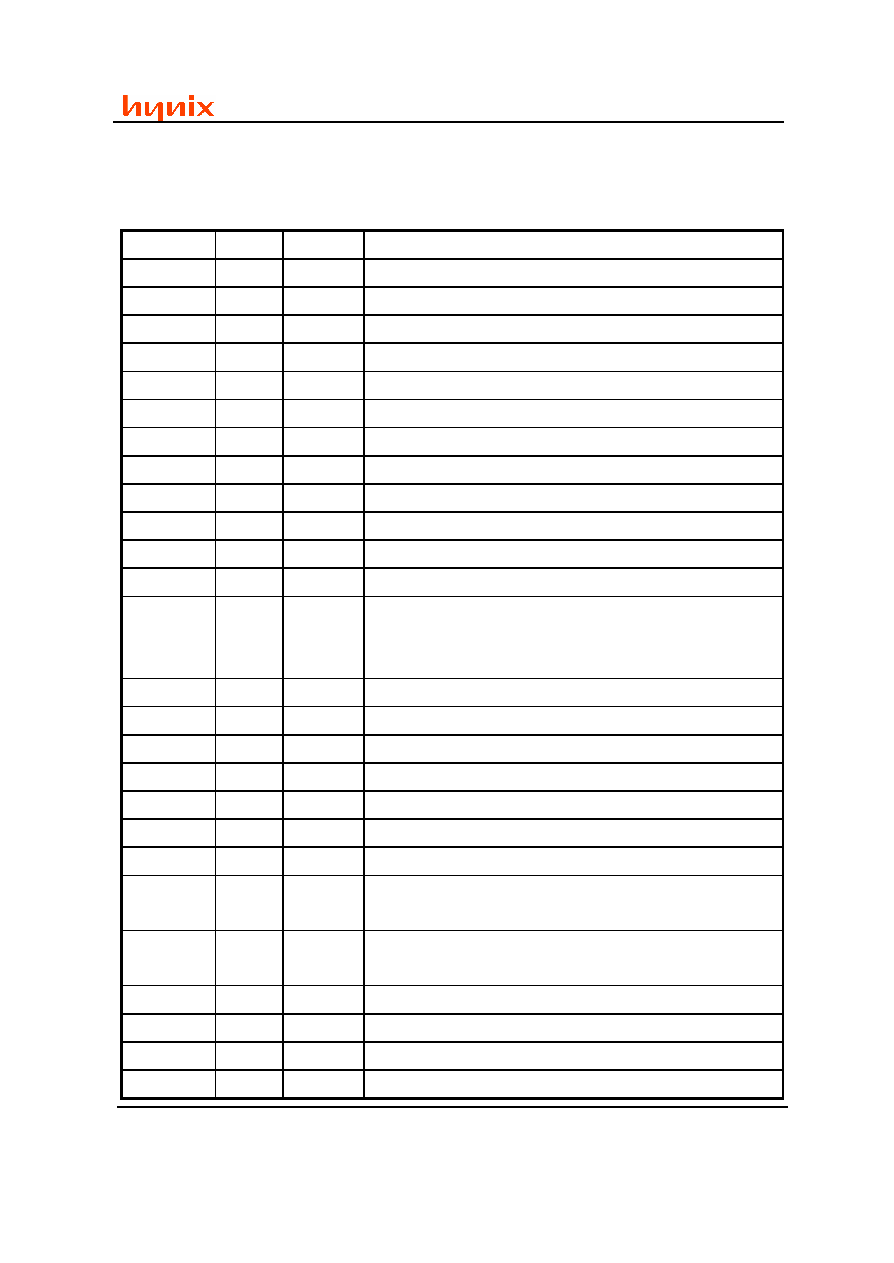
Register Description
Addres
s
Default
Symbol
(Hex)
(Hex)
Description
DEVID
00
50
Device ID
SCTRA
01
13
Sensor Control A
SCTRB
02
00
Sensor Control B
SCTRC
03
01
Sensor Control C
RSAU
08
00
Row Start Address Upper
RSAL
09
02
Row Start Address Lower
CSAU
0A
00
Column Start Address Upper
CSAL
0B
02
Column Start Address Lower
WIHU
0C
03
Window Height Upper
WIHL
0D
60
Window Height Lower
WIWU
0E
04
Window Width Upper
WIWL
0F
80
Window Width Lower
HBLU
10
00
Horizontal Blank Time Upper
HBLL
11
D0
Horizontal Blank Time Lower
VBLU
12
00
Vertical Blank Time Upper
VBLL
13
08
Vertical Blank Time Lower
RGAIN
14
08
Red Color Gain
GGAIN
15
08
Green Color Gain
BGAIN
16
08
Blue Color Gain
AMPGAIN
17
08
Amp Gain for Pixel Output
AMPMIN
18
10
Amp Gain Minimum Value
AMPMAX
19
28
Amp Gain Maximum Value
AMPNOM
1A
18
Amp Gain Normal Value
AMPBIAS
1B
13
CDS Bias , Amplifier Bias
RSTCLMP
1C
07
Reset Level Clamp Enable, Reset Value
HV7151SP
CMOS Image Sensor
Confidential
With Image Signal Processing
This document is a general product description and is subject to change without notice. Hynix
Semiconductor Inc. does not assume any responsibility for use of circuits described and no patent
licenses are implied.
- 17 -
2003 Hynix Semiconductor Inc.
ADCBIAS
20
2
ADC Bias Control
OREDI
21
7F
ADC Initial Offset Value for Optical Black Red
OGRNI
22
7F
ADC Initial Offset Value for Optical Black Green
OBLUI
23
7F
ADC Initial Offset Value for Optical Black Blue
BLKTH
27
FF
Black Level Threshold Value
ISPFUN
30
FF
Image Signal Processing Functions Enable
OUTFMT
31
31
Image Data Output Format
OUTINV
32
00
Output Signal Inversion
EDGEWT
33
02
Edge Enhancement Weight
CRCM11
34
4C
Color Correction matrix coefficient 11
CRCM12
35
EC
Color Correction matrix coefficient 12
CRCM13
36
08
Color Correction matrix coefficient 13
CRCM21
37
F0
Color Correction matrix coefficient 21
CRCM22
38
76
Color Correction matrix coefficient 22
CRCM23
39
DB
Color Correction matrix coefficient 23
CRCM31
3A
FE
Color Correction matrix coefficient 31
CRCM32
3B
E8
Color Correction matrix coefficient 32
CRCM33
3C
5A
Color Correction matrix coefficient 33
GMAP0
40
00
Start point for gamma line segment 0
GMAP1
41
04
Start point for gamma line segment 1
GMAP2
42
1C
Start point for gamma line segment 2
GMAP3
43
34
Start point for gamma line segment 3
GMAP4
44
54
Start point for gamma line segment 4
GMAP5
45
78
Start point for gamma line segment 5
GMAP6
46
90
Start point for gamma line segment 6
GMAP7
47
A4
Start point for gamma line segment 7
GMAP8
48
E0
Start point for gamma line segment 8
GMAP9
49
F4
Start point for gamma line segment 9
GMAS0
50
40
Slope value for gamma line segment 0
GMAS1
51
80
Slope value for gamma line segment 1
HV7151SP
CMOS Image Sensor
Confidential
With Image Signal Processing
This document is a general product description and is subject to change without notice. Hynix
Semiconductor Inc. does not assume any responsibility for use of circuits described and no patent
licenses are implied.
- 18 -
2003 Hynix Semiconductor Inc.
GMAS2
52
60
Slope value for gamma line segment 2
GMAS3
53
40
Slope value for gamma line segment 3
GMAS4
54
24
Slope value for gamma line segment 4
GMAS5
55
18
Slope value for gamma line segment 5
GMAS6
56
14
Slope value for gamma line segment 6
GMAS7
57
0F
Slope value for gamma line segment 7
GMAS8
58
05
Slope value for gamma line segment 8
GMAS9
59
02
Slope value for gamma line segment 9
BRIGHTY
5A
00
Brightness factor for brightness adjustment
SATCR
5B
80
Saturation factor for Saturation adjustment
SATCB
5C
80
Saturation factor for Saturation adjustment
EDTHLO
5D
05
Edge Enhancement Vth Low
EDTHHI
5E
80
Edge Enhancement Vth High
CHSUPFNC
5F
64
Chroma Suppression Function
AEMODE1
60
BD
Auto Exposure Control Mode 1
AEMODE2
61
5D
Auto Exposure Control Mode 2
CSCMODE
62
00
Color Space Conversion Mode Select
INTH
63
13
Integration Time
High
INTM
64
88
Integration Time
Middle
INTL
65
00
Integration Time
Low
AETRGT
66
70
Luminance Target Value
AELFBND
67
A2
Y frame mean value displacement boundary
AEULBND
68
2A
Y frame mean value displacement from AE target where AE update
speed transits from 2x integration unit speed to 1x integration unit
speed
ASFCON
69
00
AE Speed and Frame Control
AESTEPH
6A
02
AE Anti-Banding Step High
AESTEPM
6B
EE
AE Anti-Banding Step Middle
AESTEPL
6C
00
AE Anti-Banding Step Low
AEINTH
6D
3A
AE Integration Time Limit High
AEINTM
6E
98
AE Integration Time Limit Middle
HV7151SP
CMOS Image Sensor
Confidential
With Image Signal Processing
This document is a general product description and is subject to change without notice. Hynix
Semiconductor Inc. does not assume any responsibility for use of circuits described and no patent
licenses are implied.
- 19 -
2003 Hynix Semiconductor Inc.
AEINTL
6F
00
AE Integration Time Limit Low
AWBMODE1
70
41
Auto White Balance Control Mode 1
AWBMODE2
71
02
Auto White Balance Control Mode 2
CBTRGT
73
80
Cb Frame Mean Value for AWB.
CRTRGT
74
80
Cr Frame Mean Value for AWB.
AWBLBND
75
02
Cb, Cr Frame Mean Displacement from Cb Target and Cr Target
where AWB goes into LOCK state
AWBULBND
76
06
Displacement from ideal white pixel where AWB release from LOCK
state
AWBWBND
77
30
Displacement from ideal white pixel where AWB recognizes a pixel
as a white pixel affected by light source
AESTAT
7B
RO
Current AE Operation Status
AWBSTAT
7C
RO
Current AWB Operation Status
LUMEAN
7D
RO
Active Y Frame Mean Value
CBMEAN
7E
RO
Active Cb Frame Mean Value
CRMEAN
7F
RO
Active Cr Frame Mean Value
BNDGMIN
80
08
Minimum gain value with Anti-Banding enabled
BNDGMAX
81
18
Maximum gain value with Anti-Banding enabled
AWBWHT
8A
C8
During Cb, Cr frame mean value calculation, AWB discards pixel of
which luminance is larger than this register value.
AWBBLK
8B
0A
During Cb, Cr frame mean value calculation, AWB discards pixel of
which luminance is smaller than this register value.
AWBVALID
8C
02
AWB update when the number of valid color pixel is larger than (this
minimum value x 64)
DPCMODE
90
01
Dark Bad Pixel Concealment Mode selection
DPCINTVALH
91
29
Integration Time Value High Byte where filtering operation gets active
when dark bad pixel Concealment mode is enabled.
DPCINTVALM
92
DA
Integration Time Value Middle Byte where filtering operation gets
active when dark bad pixel Concealment mode is enabled.
DPCINTVALL
93
49
Integration Time Value Lower Byte where filtering operation gets
active when dark bad pixel Concealment mode is enabled.
DPCGTH
94
20
Neighbor-differential threshold value that specify G dark bad pixel
DPCCTH
95
20
Neighbor-differential threshold value that specify R/B dark bad pixel
DPCGAINVAL
96
38
Reference of Amp Gain which Dark Bad Pixel Concealment mode is
enabled or disabled
CONTY
97
80
Contrast factor for Contrast Adjustment
PCTRA
A0
01
PLL Control Mode A
PCTRB
A1
1D
PLL Control Mode B
PFDDIVH
A4
00
PLL Feedback Divisor High
HV7151SP
CMOS Image Sensor
Confidential
With Image Signal Processing
This document is a general product description and is subject to change without notice. Hynix
Semiconductor Inc. does not assume any responsibility for use of circuits described and no patent
licenses are implied.
- 20 -
2003 Hynix Semiconductor Inc.
PFDDIVL
A5
02
PLL Feedback Divisor Low
PXNUMH
B9
04
Pixel Number High
PXNUML
BA
00
Pixel Number Low
STTHVAL
BB
30
Stable Range Variation
CHTHVAL
BC
20
Frequency Change Variation
AFCMODE
BD
00
AFC Mode Control
INTEGT50H
C0
02
50Hz Integration Time High
INTEGT50M
C1
EE
50Hz Integration Time Middle
INTEGT50L
C2
00
50Hz Integration Time Low
INTEGT60H
C3
02
60Hz Integration Time High
INTEGT60M
C4
71
60Hz Integration Time Middle
INTEGT60L
C5
00
60Hz Integration Time Low
HV7151SP
CMOS Image Sensor
Confidential
With Image Signal Processing
This document is a general product description and is subject to change without notice. Hynix
Semiconductor Inc. does not assume any responsibility for use of circuits described and no patent
licenses are implied.
- 21 -
2003 Hynix Semiconductor Inc.
Device ID [DEVID : 00h : 50h]
7
6
5
4
3
2
1
0
Product ID
Revision Number
0
1
0
1
0
0
0
0
High Nibble represents Sensor Resolution, Low Nibble represents Revision Number.
Sensor Control A [SCTRA : 01h : 13h]
7
6
5
4
3
2
1
0
Reserved
X-Flip
Y-Flip
Video Mode
0
0
0
1
0
0
1
1
X-Flip
Image is horizontally flipped
Y-Flip
Image is vertically flipped
111 1/6 scaling QCIF mode
110 1/3 scaling CIF mode
101 5/18 scaling QVGA mode
100 5/9 scaling VGA mode
011 5x5 linear color interpolation mode
010 1/4 sub-sampling mode
001 1/16 sub-sampling mode
Video Mode
000 Bayer output mode
Sensor Control B [SCTRB : 02h : 00h]
7
6
5
4
3
2
1
0
AE/AWB
Block
Sleep
Datapath
Block
Sleep
Analog
Block
Sleep
Sleep
Mode
Strobe
Enable
Clock Division
0
0
0
0
0
0
0
0
HV7151SP
CMOS Image Sensor
Confidential
With Image Signal Processing
This document is a general product description and is subject to change without notice. Hynix
Semiconductor Inc. does not assume any responsibility for use of circuits described and no patent
licenses are implied.
- 22 -
2003 Hynix Semiconductor Inc.
AE/AWB Block Sleep AE/AWB block goes into sleep mode with this bit set to high.
Datapath Block Sleep Image processing datapath block goes into sleep mode with this bit set to
high.
Analog Block Sleep
all internal analog block goes into sleep mode with this bit set to high. With
All Digital Block Sleep active, sensor goes into power down mode.
Sleep Mode
all internal digital and analog block goes into sleep with this bit set to high.
Strobe Enable
When strobe signal is enabled by this bit, STROBE pin will indicates when
strobe light should be splashed in the dark environment to get adequate
lighted image.
Clock Division
divides input master clock(IMC) for internal use. Internal divided clock
frequency(DCF) is defined as master clock frequency(MCF) divided by
specified clock divisor. Internal divided clock frequency(DCF) is as follows.
000 : MCF, 001 : MCF/2, 010 : MCF/4, 011 : MCF/8
100 : MCF/16, 101 : MCF/32, 110 : MCF/64, 111 : MCF/128
Sensor Control C [SCTRC : 03h : 01h]
7
6
5
4
3
2
1
0
reserved
HSYNC in
VBLANK
VBLANK
Unit
Unified
Gain
Black
Level Data
Enable
Black
Level
Compens-
ation
0
0
0
0
0
0
0
1
HSYNC in VBLANK
0 : There are no valid HSYNC during valid VBLANK.
1 : There are valid HSYNC during valid VBLANK. At time, VBLANK unit must be Line unit.
VBLANK
HSYNC
VBLANK unit
0 : Line unit. VBLANK unit is based on multiple line period time of sensor.
HV7151SP
CMOS Image Sensor
Confidential
With Image Signal Processing
This document is a general product description and is subject to change without notice. Hynix
Semiconductor Inc. does not assume any responsibility for use of circuits described and no patent
licenses are implied.
- 23 -
2003 Hynix Semiconductor Inc.
1 : Pixel unit. VBLANK unit is based on multiple pixel clock period time of sensor.
Unified Gain
1 : G analog gain is used for R,G and B analog gain.
0 : R,G and B analog gain is used
individually.
Black Level Data Enable
HSYNC is generated for light-shielded pixels in 4 lines.
Black Level Compensation
Black level average values of light-shielded pixels are compensated when active image data is
produced.
Row Start Address Upper [RSAU : 08h : 00h]
7
6
5
4
3
2
1
0
Reserved
Row Start Address
Upper
0
0
0
0
0
0
0
0
Row Start Address Lower [RSAL : 09h : 02h]
7
6
5
4
3
2
1
0
Row Start Address Lower
0
0
0
0
0
0
1
0
Row Start Address register defines the row start address of image read out operation.
Column Start Address Upper [CSAU : 0ah : 00h]
7
6
5
4
3
2
1
0
Reserved
Column Start Address Upper
0
0
0
0
0
0
0
0
Column Start Address Lower [CSAL : 0bh : 02h]
7
6
5
4
3
2
1
0
HV7151SP
CMOS Image Sensor
Confidential
With Image Signal Processing
This document is a general product description and is subject to change without notice. Hynix
Semiconductor Inc. does not assume any responsibility for use of circuits described and no patent
licenses are implied.
- 24 -
2003 Hynix Semiconductor Inc.
Column Start Address Lower
0
0
0
0
0
0
1
0
Column Start Address register defines the column start address of image read out operation.
Window Height Upper [WIHU : 0ch : 03h]
7
6
5
4
3
2
1
0
Reserved
Window Height Upper
0
0
0
0
0
0
1
1
Window Height Lower [WIHL : 0dh : 60h]
7
6
5
4
3
2
1
0
Window Height Lower
0
1
1
0
0
0
0
0
Window Height register defines the height of image to be read out.
Window Width Upper [WIWU : 0eh : 04h]
7
6
5
4
3
2
1
0
Reserved
Window Width Upper
0
0
0
0
0
1
0
0
Window Width Lower [WIWL : 0fh : 80h]
7
6
5
4
3
2
1
0
Window Width Lower
1
0
0
0
0
0
0
0
Window Width Address register defines the width of image to be read out.
HV7151SP
CMOS Image Sensor
Confidential
With Image Signal Processing
This document is a general product description and is subject to change without notice. Hynix
Semiconductor Inc. does not assume any responsibility for use of circuits described and no patent
licenses are implied.
- 25 -
2003 Hynix Semiconductor Inc.
Horizontal Blank Time Upper [HBLU : 10h : 00h]
7
6
5
4
3
2
1
0
Horizontal Blank Time Upper
0
0
0
0
0
0
0
0
Horizontal Blank Time Lower [HBLL : 11h : d0h]
7
6
5
4
3
2
1
0
Horizontal Blank Time Lower
1
1
0
1
0
0
0
0
HBLANK Time register defines data blank time between current line and next line by using Sensor
Clock Period unit, and should be larger than 208(d0h).
Vertical Blank Time Upper [VBLU : 12h : 00h]
7
6
5
4
3
2
1
0
Vertical Blank Time Upper
0
0
0
0
0
0
0
0
Vertical Blank Time Lower [VBLL : 13h : 08h]
7
6
5
4
3
2
1
0
Vertical Blank Time Lower
0
0
0
0
1
0
0
0
VBLANK Time register defines active high duration of VSYNC output. Active high VSYNC indicates
frame boundary between continuous frames.
Each sensor has a little different photo-diode characteristics so that the sensor provides internal
adjustment registers that calibrates internal sensing circuit in order to get optimal performance.
Sensor characteristics adjustment registers are as below.
Red Color Gain [RGAIN : 14h : 08h]
7
6
5
4
3
2
1
0
Reserved
Red Amplifier Gain
HV7151SP
CMOS Image Sensor
Confidential
With Image Signal Processing
This document is a general product description and is subject to change without notice. Hynix
Semiconductor Inc. does not assume any responsibility for use of circuits described and no patent
licenses are implied.
- 26 -
2003 Hynix Semiconductor Inc.
0
0
0
0
1
0
0
0
Green Color Gain [GGAIN : 15h : 08h]
7
6
5
4
3
2
1
0
Reserved
Green Amplifier Gain
0
0
0
0
1
0
0
0
Blue Color Gain [BGAIN : 16h : 08h]
7
6
5
4
3
2
1
0
Reserved
Blue Amplifier Gain
0
0
0
0
1
0
0
0
There are three color gain registers for R, G, B pixels, respectively. Programmable range is from 0.5X
~ 2.5X. Effective Gain = 0.5 + B<4:0>/16. These registers may be used for white balance and color
effect with independent R,G,B color control. Default gain is 1X.
Amp Gain [AMPGAIN : 17h : 08h]
7
6
5
4
3
2
1
0
Reserved
Amp Gain
0
0
0
0
1
0
0
0
Amp Gain is common gain for R, G, B channel and used for auto exposure control. Programmable
range is from 0.5X ~ 8.5X. Default gain is 1X.
Gain = 0.5 + B<6:0>/16
Amp Gain Minimum Value [AMPMIN : 18h : 10h]
7
6
5
4
3
2
1
0
Reserved
Amp Gain Minimum
0
0
0
1
0
0
0
0
Amp Gain Minimum Value is minimum value of amplifier gain when sensor adjusts amplifier gain for
auto exposure control. Programmable range is same as Amp Gain. Recommended value is 1.5X.
Amp Gain Maximum Value [AMPMAX : 19h : 28h]
7
6
5
4
3
2
1
0
Reserved
Amp Gain Maximum
HV7151SP
CMOS Image Sensor
Confidential
With Image Signal Processing
This document is a general product description and is subject to change without notice. Hynix
Semiconductor Inc. does not assume any responsibility for use of circuits described and no patent
licenses are implied.
- 27 -
2003 Hynix Semiconductor Inc.
0
0
1
0
1
0
0
0
Amp Gain Maximum Value is maximum value of amplifier gain when sensor adjusts amplifier gain for
auto exposure control. Programmable range is same as Amp Gain. Recommended value is 3X.
Amp Gain Normal Value [AMPNOM : 1ah : 18h]
7
6
5
4
3
2
1
0
Reserved
Amp Gain Normal
0
0
0
1
1
0
0
0
Amp Gain Normal Value is reference value of amp gain when sensor adjusts amp gain for auto
exposure control. First, sensor controls integration time before adjusting amp gain for auto exposure
control. After integration time is changed to the minimum or maximum value, sensor adjusts amp gain
from this register value. Refer to figure of AE mode1 register(60H).
Programmable range is same as amp gain. Recommended value is 2X.
ASP Bias [ASPBIAS : 1bh : 13h]
7
6
5
4
3
2
1
0
Reserved
Pixel Bias
Amplifier Bias
0
0
0
1
0
0
1
1
Pixel Bias
controls the amount of current in internal pixel bias circuit to amplify pixel output
effectively. The larger register value increases the amount of current.
Amplifier Bias
controls the amount of current in internal amplifier bias circuit to amplify pixel
output effectively. The larger register value increases the amount of current.
Reset Level Clamp [RSTCLMP : 1ch : 07h]
7
6
5
4
3
2
1
0
Reserved
Clamp On
Reset Level Clamp
0
0
0
0
0
1
1
1
Because extremely bright image like sun affects reset data voltage of pixel to lower, bright image is
captured as black image in image sensor regardless of correlated double sampling. To solve this
extraordinary phenomenon, we adopt the method to clamp reset data voltage. Reset Level Clamp
HV7151SP
CMOS Image Sensor
Confidential
With Image Signal Processing
This document is a general product description and is subject to change without notice. Hynix
Semiconductor Inc. does not assume any responsibility for use of circuits described and no patent
licenses are implied.
- 28 -
2003 Hynix Semiconductor Inc.
controls the reset data voltage to prevent inversion of extremely bright image. The larger register value
clamps the reset data level at highest voltage level. Default value is 7 to clamp the reset data level at
appropriate voltage level.
ADC Bias [ADCBIAS : 20h : 02h]
7
6
5
4
3
2
1
0
Reserved
ADC Bias
0
0
0
0
0
0
1
0
ADC Bias controls the amount of current in ADC bias circuit to operate ADC effectively.
ADC Initial Offset Value for Optical Black Red [OREDI : 21h : 7fh]
7
6
5
4
3
2
1
0
Red Pixel Black Offset
0
1
1
1
1
1
1
1
ADC Initial Offset Value for Optical Black Green [OGRNI : 22h : 7fh]
7
6
5
4
3
2
1
0
Green Pixel Black Offset
0
1
1
1
1
1
1
1
ADC Initial Offse t Value for Optical Black Blue [OBLUI : 23h : 7fh]
7
6
5
4
3
2
1
0
Blue Pixel Black Offset
0
1
1
1
1
1
1
1
These registers control the offset voltage of ADC that changes the black level value for light-shielded
pixels, R,G,B respectively. Register bit functions are composed as follows.
Pixel Black Offset[7]
The bit specifies whether to subtract or add offset voltage in ADC input for
light-shielded pixels.
Pixel Black Offset[6:0] This value specifies the amount of offset voltage for light-shielded pixels.

HV7151SP
CMOS Image Sensor
Confidential
With Image Signal Processing
This document is a general product description and is subject to change without notice. Hynix
Semiconductor Inc. does not assume any responsibility for use of circuits described and no patent
licenses are implied.
- 29 -
2003 Hynix Semiconductor Inc.

HV7151SP
CMOS Image Sensor
Confidential
With Image Signal Processing
This document is a general product description and is subject to change without notice. Hynix
Semiconductor Inc. does not assume any responsibility for use of circuits described and no patent
licenses are implied.
- 30 -
2003 Hynix Semiconductor Inc.
Black Level Threshold Value [BLKTH : 27h : ffh]
7
6
5
4
3
2
1
0
Black Level Threshold
1
1
1
1
1
1
1
1
The register specifies the maximum value that determines whether light-shielded pixel output is valid.
When light-shielded pixel output exceeds this limit, the pixel is not accounted for black level
calculation.

HV7151SP
CMOS Image Sensor
Confidential
With Image Signal Processing
This document is a general product description and is subject to change without notice. Hynix
Semiconductor Inc. does not assume any responsibility for use of circuits described and no patent
licenses are implied.
- 31 -
2003 Hynix Semiconductor Inc.
ISP Function Enable [ISPFUN : 30h : ffh]
7
6
5
4
3
2
1
0
Reserved
Contrast
Adjustment
Chroma
Suppression
Edge
Enhancement
Color Space
Conversion
Color
Correction
Color
Interpolation
Gamma
Correction
0
1
1
1
1
1
1
1
Contrast Adjustment
0 : Disable.
1 : Enable. Y Output multiplied by Contrast factor
Chroma Suppression
0 : Disable.
1 : Enable. Chroma Suppressed Cb,Cr Output
Edge Enhancement
0 : Disable.
1 : Enable.
Color Space Conversion
0 : Disable. R,G,B Output
1 : Enable. Y,Cb,Cr Output
Color Correction
0 : Disable.
1 : Enable.
Color Interpolation
0 : Disable.
1 : Enable.
Gamma Correction
0 : Disable. Normal Bayer Output
1 : Enable. Gamma Corrected Bayer Output
HV7151SP
CMOS Image Sensor
Confidential
With Image Signal Processing
This document is a general product description and is subject to change without notice. Hynix
Semiconductor Inc. does not assume any responsibility for use of circuits described and no patent
licenses are implied.
- 32 -
2003 Hynix Semiconductor Inc.
Output Format [OUTFMT : 31h : 31h]
7
6
5
4
3
2
1
0
Gamma-
Corrected
Bayer
Bayer 8bit
Output
Cb/B First
Y First
YCbCr
4:4:4 / 4:2:2
RGB
4:4:4
RGB 565
8 bit Output
0
0
1
1
0
0
0
1
Gamma-Corrected
Bayer
Gamma-corrected Bayer data are output when Bayer mode is set in SCTRA
register.
Bayer 8bit Output
Bayer data is output with 8bit mode, two LSB of 11 bit Bayer data is stripped
out.
Cb/B First
Cb(B) pixel in front of Cr(R) pixel in 16bit or 8bit video data output modes.
Y First
Y pixel in front of Cb and Cr pixels in 8bit video output mode. This option is
meaningful only with YCbCr 4:2:2 8bit output mode.
YCbCr
4:4:4 / 4:2:2
This bit is high, output format is YCbCr 4:4:4 16bit mode, otherwise output
format is YCbCr 4:2:2 8bit/16bit mode.
RGB 4:4:4
R,G,B 24bit data for a pixel is produced with 16bit output mode.
RGB 565
Data format of RGB 565 mode is composed with {R[7:3]/G[7:5]} ,
{G[4:2]/B[7:3]} or {B[7:3]/G[7:5]}, {G[4:2]/R[7:3]}. OUTFMT[5](Cb/B First)
register affects above data form.
8 Bit Output
Image Data is produced only in Y[7:0]. C[7:0] should be discarded.
Default mode of Output Format is YCbCr 4:2:2 8bit mode.
Output Signal Inversion [OUTINV : 32h : 00h]
7
6
5
4
3
2
1
0
Reserved
Clocked
HSYNC
VSYNC
inversion
HSYNC
inversion
VCLK
inversion
0
0
0
0
0
0
0
0
Clocked HSYNC
In HSYNC, VCLK is embedded, that is, HSYNC is toggling at VCLK rate
during normal HSYNC time
VSYNC inversion
VSYNC output polarity is inverted
HSYNC inversion
HSYNC output polarity is inverted
HV7151SP
CMOS Image Sensor
Confidential
With Image Signal Processing
This document is a general product description and is subject to change without notice. Hynix
Semiconductor Inc. does not assume any responsibility for use of circuits described and no patent
licenses are implied.
- 33 -
2003 Hynix Semiconductor Inc.
VCLK inversion
VCLK output polarity is inverted
Edge Enhancement Weight [EDGEWT : 33h : 02h]
7
6
5
4
3
2
1
0
Reserved
Edge Enhancement Weight
0
0
0
0
0
0
1
0
Edge Enhancement Weight range is 0.3(3'h000) ~ 1(3'h111), and default value is 0.5(3'h010). As
Edge Enhancement Weight is large, the effect of Edge Enhancement grows stronger.
Color Correction Matrix Coefficient 11 [CRCM11 : 34h : 4ch]
7
6
5
4
3
2
1
0
Color Correction Matrix Coefficient 11
0
1
0
0
1
1
0
0
Color Correction Matrix Coefficient 12 [CRCM 12 : 35h : ech]
7
6
5
4
3
2
1
0
Color Correction Matrix Coefficient 12
1
1
1
0
1
1
0
0
Color Correction Matrix Coefficient 13 [CRCM 13 : 36h : 08h]
7
6
5
4
3
2
1
0
Color Correction Matrix Coefficient 13
0
0
0
0
1
0
0
0
Color Correction Matrix Coefficient 21 [CRCM 21 : 37h : f0h]
7
6
5
4
3
2
1
0
Color Correction Matrix Coefficient 21
1
1
1
1
0
0
0
0
HV7151SP
CMOS Image Sensor
Confidential
With Image Signal Processing
This document is a general product description and is subject to change without notice. Hynix
Semiconductor Inc. does not assume any responsibility for use of circuits described and no patent
licenses are implied.
- 34 -
2003 Hynix Semiconductor Inc.
Color Correction Matrix Coefficient 22 [CRCM 22 : 38h : 76h]
7
6
5
4
3
2
1
0
Color Correction Matrix Coefficient 22
0
1
1
1
0
1
1
0
Color Correction Matrix Coefficient 23 [CRCM 23 : 39h : dbh]
7
6
5
4
3
2
1
0
Color Correction Matrix Coefficient 23
1
1
0
1
1
0
1
1
Color Correction Matrix Coefficient 31 [CRCM 31 : 3ah : feh]
7
6
5
4
3
2
1
0
Color Correction Matrix Coefficient 31
1
1
1
1
1
1
1
0
Color Correction Matrix Coefficient 32 [CRCM 32 : 3bh : e8h]
7
6
5
4
3
2
1
0
Color Correction Matrix Coefficient 32
1
1
1
0
1
0
0
0
Color Correction Matrix Coefficient 33 [CRCM 33 : 3ch : 5ah]
7
6
5
4
3
2
1
0
Color Correction Matrix Coefficient 33
0
1
0
1
1
0
1
0
Gamma Segment Start Points
HV7151SP
CMOS Image Sensor
Confidential
With Image Signal Processing
This document is a general product description and is subject to change without notice. Hynix
Semiconductor Inc. does not assume any responsibility for use of circuits described and no patent
licenses are implied.
- 35 -
2003 Hynix Semiconductor Inc.
Gamma Segment Start Points specify the start points of nine line segments for piecewise gamma
approximation. Current default gamma curve is very selected for optimum gray gradation.
Gamma Point 0 [GAMP0 : 40h : 00h]
7
6
5
4
3
2
1
0
Gamma Point 0
0
0
0
0
0
0
0
0
Gamma Point 1 [GMAP1 : 41h : 04h]
7
6
5
4
3
2
1
0
Gamma Point 1
0
0
0
0
0
1
0
0
Gamma Point 2 [GMAP2 : 42h : 1ch]
7
6
5
4
3
2
1
0
Gamma Point 2
0
0
0
1
1
1
0
0
Gamma Point 3 [GMAP3 : 43h : 34h]
7
6
5
4
3
2
1
0
Gamma Point 3
0
0
1
1
0
1
0
0
Gamma Point 4 [GMAP4 : 44h : 54h]
7
6
5
4
3
2
1
0
Gamma Point 4
0
1
0
1
0
1
0
0
Gamma Point 5 [GMAP5 : 45h : 78h]
HV7151SP
CMOS Image Sensor
Confidential
With Image Signal Processing
This document is a general product description and is subject to change without notice. Hynix
Semiconductor Inc. does not assume any responsibility for use of circuits described and no patent
licenses are implied.
- 36 -
2003 Hynix Semiconductor Inc.
7
6
5
4
3
2
1
0
Gamma Point 5
0
1
1
1
1
0
0
0
Gamma Point 6 [GMAP6 : 46h : 90h]
7
6
5
4
3
2
1
0
Gamma Point 6
1
0
0
1
0
0
0
0
Gamma Point 7 [GMAP7 : 47h : a4h]
7
6
5
4
3
2
1
0
Gamma Point 7
1
0
1
0
0
1
0
0
Gamma Point 8 [GMAP8 : 48h : e0h]
7
6
5
4
3
2
1
0
Gamma Point 8
1
1
1
0
0
0
0
0
Gamma Point 9 [GMAP9 : 49h : f4h]
7
6
5
4
3
2
1
0
Gamma Point 9
1
1
1
1
0
1
0
0
Gamma Slope 0 [GMAS0 : 50h : 40h]
7
6
5
4
3
2
1
0
Gamma Slope 0
0
1
0
0
0
0
0
0
HV7151SP
CMOS Image Sensor
Confidential
With Image Signal Processing
This document is a general product description and is subject to change without notice. Hynix
Semiconductor Inc. does not assume any responsibility for use of circuits described and no patent
licenses are implied.
- 37 -
2003 Hynix Semiconductor Inc.
Gamma Slope 1 [GMAS1 : 51h : 80h]
7
6
5
4
3
2
1
0
Gamma Slope 1
1
0
0
0
0
0
0
0
Gamma Slope 2 [GMAS2 : 52h : 60h]
7
6
5
4
3
2
1
0
Gamma Slope 2
0
1
1
0
0
0
0
0
Gamma Slope 3 [GMAS3 : 53h : 40h]
7
6
5
4
3
2
1
0
Gamma Slope 3
0
1
0
0
0
0
0
0
Gamma Slope 4 [GMAS4 : 54h : 24h]
7
6
5
4
3
2
1
0
Gamma Slope 4
0
0
1
0
0
1
0
0
Gamma Slope 5 [GMAS5 : 55h : 18h]
7
6
5
4
3
2
1
0
Gamma Slope 5
0
0
0
1
1
0
0
0
Gamma Slope 6 [GMAS6 : 56h : 14h]
7
6
5
4
3
2
1
0
Gamma Slope 6
0
0
0
1
0
1
0
0
HV7151SP
CMOS Image Sensor
Confidential
With Image Signal Processing
This document is a general product description and is subject to change without notice. Hynix
Semiconductor Inc. does not assume any responsibility for use of circuits described and no patent
licenses are implied.
- 38 -
2003 Hynix Semiconductor Inc.
Gamma Slope 7 [GMAS7 : 57h : 0fh]
7
6
5
4
3
2
1
0
Gamma Slope 7
0
0
0
0
1
1
1
1
Gamma Slope 8 [GMAS8 : 58h : 05h]
7
6
5
4
3
2
1
0
Gamma Slope 8
0
0
0
0
0
1
0
1
Gamma Slope 9 [GMAS9 : 59h : 02h]
7
6
5
4
3
2
1
0
Gamma Slope 9
0
0
0
0
0
0
1
0
Brightness Factor Y [BRIGHTY : 5ah : 00h]
7
6
5
4
3
2
1
0
Brightness Factor Y
0
0
0
0
0
0
0
0
Brightness Adjustment is performed for summing Y data and Brightness Factor Y. Brightness Factor
Y is two's complement and its range is 128 ~ 127.
Bright Y = Y data + Brightness Factor Y.
for positive values, B<7:0> = Integer;
for negative values, B<7:0> = Two's Complement(Integer);
Saturation Factor Cr [SATCR : 5bh : 80h]
7
6
5
4
3
2
1
0
Saturation Factor Cr
1
0
0
0
0
0
0
0
HV7151SP
CMOS Image Sensor
Confidential
With Image Signal Processing
This document is a general product description and is subject to change without notice. Hynix
Semiconductor Inc. does not assume any responsibility for use of circuits described and no patent
licenses are implied.
- 39 -
2003 Hynix Semiconductor Inc.
Saturation Factor Cb [SATCB : 5ch : 80h]
7
6
5
4
3
2
1
0
Saturation Factor Cb
1
0
0
0
0
0
0
0
Saturation Adjustment is performed for multiplying Cr,Cb data by Saturation Factor Cr,Cb,
respectively. Programmable range of Saturation Factor Cb,Cr is 0 ~ 2.
For instant, Sat Cb = Cb data * B<7:0>/128.
Edge Enhancement Threshold Low [EDTHLO : 5dh : 05h]
7
6
5
4
3
2
1
0
Edge Enhancement Threshold Low
0
0
0
0
0
1
0
1
Edge Enhancement Threshold High [EDTHHI : 5eh : 80h]
7
6
5
4
3
2
1
0
Edge Enhancement Threshold High
1
0
0
0
0
0
0
0
Chroma Suppression Function [CHSUPFNC : 5fh : 64h]
7
6
5
4
3
2
1
0
Saturation Level
Suppression Gain Minimum
0
1
1
0
0
1
0
0
11 0% of difference between Current Cb,Cr data and reference Cb,Cr level. So,
Chroma Suppressed Cb,Cr data are equal to Current Cb,Cr data.
10 25% of difference between Current Cb,Cr data and reference Cb,Cr level.
01 50% of difference between Current Cb,Cr data and reference Cb,Cr level.
Saturation Level
00 75% of difference between Current Cb,Cr data and reference Cb,Cr level.
Suppression Gain
Minimum
When Amp Gain is greater than Suppression Gain Minimum, Chroma
Suppression Function is started.

HV7151SP
CMOS Image Sensor
Confidential
With Image Signal Processing
This document is a general product description and is subject to change without notice. Hynix
Semiconductor Inc. does not assume any responsibility for use of circuits described and no patent
licenses are implied.
- 40 -
2003 Hynix Semiconductor Inc.
HV7151SP
CMOS Image Sensor
Confidential
With Image Signal Processing
This document is a general product description and is subject to change without notice. Hynix
Semiconductor Inc. does not assume any responsibility for use of circuits described and no patent
licenses are implied.
- 41 -
2003 Hynix Semiconductor Inc.
Auto Exposure
Y mean value is continuously calculated every frame, and the integration time value is increased or
decreased according to the displacement between current frame Y mean value and target Y mean
value.
AE Unlock Boundary [68h]
AE Target [66h]
AE Lock Boundary [67h]
AE Lock Boundary [67h]
AE Unlock Boundary [68h]
80h
Y Frame Mean
FFh
0h
AE Mode Control 1 [AEMODE1 : 60h : bdh]
7
6
5
4
3
2
1
0
Anti
Banding
Enable
Full
Window
Window Mode
AE speed
AE Mode
1
0
1
1
1
1
0
1
HV7151SP
CMOS Image Sensor
Confidential
With Image Signal Processing
This document is a general product description and is subject to change without notice. Hynix
Semiconductor Inc. does not assume any responsibility for use of circuits described and no patent
licenses are implied.
- 42 -
2003 Hynix Semiconductor Inc.
Anti-Banding Enable
When Anti-Banding is enabled, AE initializes Integration Time registers[63h-
65h] to 4 x Anti-Banding Step value[6ah-6ch], and integration
increment/decrement amount is set to Anti-Banding Step value in order to
remove banding noise caused by intrinsic energy waveform of light sources.
Banding noise is inherent in CMOS image sensor that adopts rolling shutter
scheme for image acquisition. In this mode, AE operates with very large unit,
typically a reciprocal of (2 x power line frequency), so that minute integration
time tuning is not liable. Therefore, this mode is recommended for only indoor
use.
Full Window
With this bit set to high, window mode is discarded and full image data is
accounted for AE Y frame mean evaluation
11
1/8 center weighted window mode. Weighting ratio is 8:1 for inside
area vs. outside area
10
1/8 center only window mode.
01
1/4 center weighted window mode. Weighting ratio is 4:1 for inside
area vs. outside area
Window Mode
00
1/4 center only window mode.
AE Speed
(fast)11 10 01 00(slow)
11
Gain-Only control mode. Only preamp gain is controlled to get
optimum exposure state.
10
Time-Only control mode. Only integration time is controlled to get
optimum exposure state.
01
Time-Gain control mode. Integration time and preamp gain are
controlled to get optimum exposure state.
AE Mode
00
AE function is disabled
AE Mode Control 2 [AEMODE2 : 61h : 5dh]
7
6
5
4
3
2
1
0
Reserved
Gain Speed
Integration
Time Fine
Tune
Amp
Gain Fine
Tune
Anti-
Banding
Minimum
Break
AE Sub-
sampling
mode
AE Analog
Gain
Control
0
1
0
1
1
1
0
1
HV7151SP
CMOS Image Sensor
Confidential
With Image Signal Processing
This document is a general product description and is subject to change without notice. Hynix
Semiconductor Inc. does not assume any responsibility for use of circuits described and no patent
licenses are implied.
- 43 -
2003 Hynix Semiconductor Inc.
Gain Speed
Gain update speed is specified as follows.
(fast)11 10 01 00(slow)
Integration Time Fine
Tune
Integration time fine tuning is performed when AE arrive around AE Fine Tune
Boundary to settle into AE lock state smoothly.
Amp Gain Fine Tune
Amp gain fine tuning is performed when AE arrive around AE Fine Tune
Boundary to settle into AE lock state smoothly.
Anti-Banding Minimum
Break
When AE is still of out lock state despite that AE preamp analog gain update
value exceeds preamp minimum gain value(18h) and integration time(63h-
65h) is reached to AE Anti-Banding Step(6ah-6ch), integration time(63h-65h)
is broken to less than AE Anti-Banding Step(6ah-6ch).
AE Sub-sampling
Mode
AE statistics is executed on 1/4 of original image data to save power
consumption
AE Analog Gain
Control
AE updates Amp gain register(17h) in order to reach optimum exposure state
Color Space Conversion Mode [CSCMODE : 62h : 00h]
7
6
5
4
3
2
1
0
Reserved
CSC Mode
Reserved
0
0
0
1
0
0
0
0
CSC Mode
0 : Mode 1
1 : Mode 2
Integration Time High [INTH: 63h : 13h]
7
6
5
4
3
2
1
0
Integration Time Higher
0
0
0
1
0
0
1
1
HV7151SP
CMOS Image Sensor
Confidential
With Image Signal Processing
This document is a general product description and is subject to change without notice. Hynix
Semiconductor Inc. does not assume any responsibility for use of circuits described and no patent
licenses are implied.
- 44 -
2003 Hynix Semiconductor Inc.
Integration Time Middle [INTM: 64h: 88h]
7
6
5
4
3
2
1
0
Integration Time Middle
1
0
0
0
1
0
0
0
Integration Time Low [INTL: 65h: 00h]
7
6
5
4
3
2
1
0
Integration Time Lower
0
0
0
0
0
0
0
0
Integration time value register defines the time which active pixel element evaluates photon energy
that is converted to digital data output by internal ADC processing. Integration time is equivalent to
exposure time of general camera so that integration time needs to be increased in dark environment
and decreased according to lighting condition. Maximum integration time is register maximum
value(2
24
-1) x sensor clock period (52ns, SCF 19.2Mhz) = 0.87sec.
SCF = Sensor Clock Frequency
Luminance Target Value [AETRGT : 66h : 70h]
7
6
5
4
3
2
1
0
Luminance Target
0
1
1
1
0
0
0
0
This register defines the target luminance value for AE operation.
AE Lock & Fine Tune Boundary [AELFBND : 67h : a2h]
7
6
5
4
3
2
1
0
AE Fine Boundary
AE Lock Boundary
1
0
1
0
0
0
1
0
AE Lock Boundary specifies the displacement of Y Frame Mean value(7dh) from AE Target in which
AE goes into LOCK state. With Anti-Banding is enabled, this displacement condition is discarded,
and instead AE Speed Unlock Boundary is used as Lock boundary.
AE Fine Boundary specifies the displacement of Y Frame Mean value(7dh) from AE Target in which
HV7151SP
CMOS Image Sensor
Confidential
With Image Signal Processing
This document is a general product description and is subject to change without notice. Hynix
Semiconductor Inc. does not assume any responsibility for use of circuits described and no patent
licenses are implied.
- 45 -
2003 Hynix Semiconductor Inc.
AE start to tune fine integration time or amp gain in order to goes into lock state smoothly.
AE Unlock Boundary [AEULBND : 68h : 2ah]
7
6
5
4
3
2
1
0
AE Unlock Boundary
0
0
1
0
1
0
1
0
AE Speed Boundary 0 specifies Y Frame Mean displacement from AE Target where integration time
increment/decrement speed changes from 2x (integration unit step) to 1x (integration unit step). In
anti-banding mode, this boundary is used as lock boundary for exposure control.
AE Speed and Frame Control [ASFCON : 69h : 00h]
7
6
5
4
3
2
1
0
Reserved
AE Speed 2
Y Frame Control
Cb,Cr Frame Control
0
0
0
0
0
0
0
0
AE Speed 2
(fast)11 10 01 00(slow)
11
4 Frame mean Value. ( For AE )
10
2 Frame mean Value.
Y Frame Control
01, 00 1 Frame mean Value.
11
4 Frame mean Value. ( For AWB )
10
2 Frame mean Value.
Cb,Cr Frame Control
01, 00 1 Frame mean Value.
AE Speed 2 is different in use to AE Speed 1. When Y Frame Mean is out of Unlock boundary, AE
updates quickly Amp Gain register(17h) in order to reach Lock boundary state.
Gain update speed is specified as follows.
(fast)11 10 01 00(slow)
Frame Control register can be use 1, 2, 4 Frame mean Value. 4 Frame mean value has a history
component of previous 3 Frame mean Value. To use 1 Frame mean Value is that AE changed every
Frame instantly.
HV7151SP
CMOS Image Sensor
Confidential
With Image Signal Processing
This document is a general product description and is subject to change without notice. Hynix
Semiconductor Inc. does not assume any responsibility for use of circuits described and no patent
licenses are implied.
- 46 -
2003 Hynix Semiconductor Inc.
AE Anti-Banding Step High [AESTEPH : 6ah : 02h]
7
6
5
4
3
2
1
0
Reserved
Integration Step Higher
0
0
0
0
0
0
1
0
AE Anti-Banding Step Middle [AESTEPM : 6bh : eeh]
7
6
5
4
3
2
1
0
Integration Step Middle
1
1
1
0
1
1
1
0
AE Anti-Banding Step Low [AESTEPL : 6ch : 00h]
7
6
5
4
3
2
1
0
Integration Step Lower
0
0
0
0
0
0
0
0
AE Anti-Banding Step specifies integration time unit value that AE uses when Anti-Banding is enabled.
Anti-Banding Step value is resolved by the following equation.
Anti-Banding Step Value = Sensor Operation Frequency (SCF) / (2x power line frequency)
The default value is set with SCF 19.2Mhz, 50Hz power line, that is,
Anti-Banding Step Value = 19.2Mhz / (2 x 50) = 192000d = 02ee00h
AE Integration Time Limit High [AEINTH : 6dh : 3ah]
7
6
5
4
3
2
1
0
AE Integration Time Limit Higher
0
0
1
1
1
0
1
0
AE Integration Time Limit Middle [AEINTM : 6eh : 98h]
7
6
5
4
3
2
1
0
HV7151SP
CMOS Image Sensor
Confidential
With Image Signal Processing
This document is a general product description and is subject to change without notice. Hynix
Semiconductor Inc. does not assume any responsibility for use of circuits described and no patent
licenses are implied.
- 47 -
2003 Hynix Semiconductor Inc.
AE Integration Time Limit Middle
1
0
0
1
1
0
0
0
AE Integration Time Limit Low [AEINTL : 6fh : 00h]
7
6
5
4
3
2
1
0
AE Integration Time Limit Lower
0
0
0
0
0
0
0
0
These three registers define the maximum integration time value that is allowed to sensor operation. It
is desirable to set the value to multiples of AE Anti-Banding Step to easily operate with Anti-banding
mode enabled. The default value is set to 1/5sec with SCF set to 19.2Mhz
19.2Mhz / 5 = 3840500d = 3a9800h
HV7151SP
CMOS Image Sensor
Confidential
With Image Signal Processing
This document is a general product description and is subject to change without notice. Hynix
Semiconductor Inc. does not assume any responsibility for use of circuits described and no patent
licenses are implied.
- 48 -
2003 Hynix Semiconductor Inc.
Auto White Balance
Cb/Cr frame mean value is calculated every frame and according to Cb/Cr frame mean values'
displacement from Cb/Cr white target point, R/B scaling values for R/B data are resolved.
AWB Unlock Boundary [76h]
Cb/Cr Target [73h-74h]
AWB Lock Boundary [75h]
AWVB White Pixel Boundary [77h]
AWB Lock Boundary [75h]
AWB Unlock Boundary [76h]
AWB White Pixel Boundary [77h]
80h
Cb/Cr Frame Mean
FFh
0h
AWB Mode Control 1 [AWBMODE1 : 70h : 41h]
7
6
5
4
3
2
1
0
Reserved
Full
Window
Reserved
Window
Mode
AWB speed
Reserved
AWB On
0
1
0
0
0
0
0
1
Full Window
With this bit set to high, window mode is discarded and full image data is
accounted for AE Y frame mean evaluation
1
1/4 center weighted window mode. Weighting ratio is 4:1 for inside
area vs. outside area
Window Mode
0
1/4 center only window mode.
AWB Speed
(Fast)11 - 10 - 01 - 00(slow)
AWB On
Auto White Balance Control Enabled
HV7151SP
CMOS Image Sensor
Confidential
With Image Signal Processing
This document is a general product description and is subject to change without notice. Hynix
Semiconductor Inc. does not assume any responsibility for use of circuits described and no patent
licenses are implied.
- 49 -
2003 Hynix Semiconductor Inc.
AWB Mode Control 2 [AEMODE2 : 71h : 02h]
7
6
5
4
3
2
1
0
Reserved
AWB Low
Speed
AWB Sub-
sampling
mode
AWB
Analog
Gain
Control
Reserved
0
0
0
0
0
0
1
0
AWB Low Speed
With this bit set to high, analog gain speed is decreased to 1/4 of the normal
speed.
AWB Sub-sampling
Mode
AWB statistics is executed on 1/4 of original image data to save power
consumption
AWB Analog Gain
Control
AWB updates R/B gain registers(14h,16h) in order to reach optimum white
balance state
Cb Frame Mean Value [CBTRGT : 73h : 80h]
7
6
5
4
3
2
1
0
Cb Frame Mean
1
0
0
0
0
0
0
0
This register defines Cb target frame mean value for AWB operation.
Cr Frame Mean Value [CRTRGT : 74h : 80h]
7
6
5
4
3
2
1
0
Cr Frame Mean
1
0
0
0
0
0
0
0
This register defines Cr target frame mean value for AWB operation.
AWB Lock Boundary [AWBLBND : 75h : 02h]
7
6
5
4
3
2
1
0
Reserved
AWB Lock Boundary
0
0
0
0
0
0
1
0
It specifies Cb/Cr frame mean values' displacement from Cb/Cr Target (73h-74h) value where AWB
HV7151SP
CMOS Image Sensor
Confidential
With Image Signal Processing
This document is a general product description and is subject to change without notice. Hynix
Semiconductor Inc. does not assume any responsibility for use of circuits described and no patent
licenses are implied.
- 50 -
2003 Hynix Semiconductor Inc.
goes into LOCK state.
AWB Unlock Boundary [AWBULBND : 76h : 06h]
7
6
5
4
3
2
1
0
AWB Unlock Boundary
0
0
0
0
0
1
1
0
It specifies Cb/Cr frame mean values' displacement from Cb/Cr Target (73h-74h) where AWB is
released from LOCK state. AWB operation retains LOCK state unless Cb/Cr frame mean values'
displacement value exceeds this boundary. The value should be larger AWB Lock Boundary.
AWB White Pixel Boundary [AWBWBND : 77h : 30h]
7
6
5
4
3
2
1
0
AWB White Pixel Boundary
0
0
1
1
0
0
0
0
When Cb/Cr frame mean values' displacement from Cb/Cr Target exceeds AWB White Pixel
Boundary value, AWB accept frame color as it is and does not try to correct white balance deviation.
Current AE Operation Status [AESTAT : 7bh : RO]
7
6
5
4
3
2
1
0
AE Mode State
AE Lock state
RO
RO
RO
RO
RO
RO
RO
RO
AE Mode State This nibble represents the mode where internal Y plane FSM is currently placed
among time-gain control, time-only control, or gain-only control modes.
AE Lock State Y channel FSM status, "0000" means that AE Y plane is in lock state
Current AWB Operation Status [AWBSTAT : 7ch : RO]
7
6
5
4
3
2
1
0
reserved
AE/AWB
Lock
Cb Lock State
Cr Lock State
RO
RO
RO
RO
RO
RO
RO
RO
HV7151SP
CMOS Image Sensor
Confidential
With Image Signal Processing
This document is a general product description and is subject to change without notice. Hynix
Semiconductor Inc. does not assume any responsibility for use of circuits described and no patent
licenses are implied.
- 51 -
2003 Hynix Semiconductor Inc.
AE/AWB Lock This single status bit indicates that AE and AWB are in lock state for optimum still
image capture.
Cb Lock State
Cb channel FSM status. "00" means that AWB Cb plane is in lock state
Cr Lock State
Cr channel FSM status. "00" means that AWB Cr plane is in lock state
Active Y Frame Mean Value [LUMEAN : 7dh : RO]
7
6
5
4
3
2
1
0
Y Frame Mean
RO
RO
RO
RO
RO
RO
RO
RO
The register reports current Y plane frame mean value.
Active Cb Frame Mean Value [CBMEAN : 7eh : RO]
7
6
5
4
3
2
1
0
Cb Frame Mean
RO
RO
RO
RO
RO
RO
RO
RO
The register reports current Cb plane frame mean value.
Active Cr Frame Mean Value [CRMEAN : 7fh : RO]
7
6
5
4
3
2
1
0
Cr Frame Mean
RO
RO
RO
RO
RO
RO
RO
RO
The register reports current Cr plane frame mean value.
Minimum Anti-Banding Gain [BNDGMIN : 80h : 08h]
7
6
5
4
3
2
1
0
Minimum Anti-Banding Gain
0
0
0
0
1
0
0
0
The register specifies the minimum limit to which AE may decrease preamp gain or Y digital gain in
order to get optimum exposure value while Anti-Banding Mode is enabled and the following condition
is met.

HV7151SP
CMOS Image Sensor
Confidential
With Image Signal Processing
This document is a general product description and is subject to change without notice. Hynix
Semiconductor Inc. does not assume any responsibility for use of circuits described and no patent
licenses are implied.
- 52 -
2003 Hynix Semiconductor Inc.
AE Lock Boundary < (Y Frame Mean - AE Target) < AE Unlock Boundary.
HV7151SP
CMOS Image Sensor
Confidential
With Image Signal Processing
This document is a general product description and is subject to change without notice. Hynix
Semiconductor Inc. does not assume any responsibility for use of circuits described and no patent
licenses are implied.
- 53 -
2003 Hynix Semiconductor Inc.
Maximum Anti-Banding Gain [BNDGMAX : 81h : 18h]
7
6
5
4
3
2
1
0
Maximum Anti-Banding Gain
0
0
0
1
1
0
0
0
The register specifies the maximum limit to which AE may increase preamp gain or Y digital gain in
order to get optimum exposure value while Anti-Banding Mode is enabled and the following condition
is met.
AE Lock Boundary < (AE Target - Y Frame Mean) < AE Unlock Boundary.
AWB Luminance Higher Limit [AWBWHT : 8ah : c8h]
7
6
5
4
3
2
1
0
AWB Luminance Higher Limit
1
1
0
0
1
0
0
0
During Cb/Cr frame mean value calculation, AWB discards pixel of which luminance value is larger
than this register value.
AWB Luminance Lower Limit [AWBBLK : 8bh : 0ah]
7
6
5
4
3
2
1
0
AWB Luminance Lower Limit
0
0
0
0
1
0
1
0
During Cb/Cr frame mean value calculation, AWB discards pixel of which luminance value is smaller
than this register value.
AWB Valid Number of Pixel [AWBVALID : 8ch : 02h]
7
6
5
4
3
2
1
0
AWB Valid Number of Pixel
0
0
0
0
0
0
1
0
AWB update when the number of valid color pixel is larger than (this valid value x 64).
HV7151SP
CMOS Image Sensor
Confidential
With Image Signal Processing
This document is a general product description and is subject to change without notice. Hynix
Semiconductor Inc. does not assume any responsibility for use of circuits described and no patent
licenses are implied.
- 54 -
2003 Hynix Semiconductor Inc.
Dark Bad Pixel Concealment Mode [DPCMODE : 90h : 01h]
7
6
5
4
3
2
1
0
Reserved
Dark Bad Pixel
Concealment Mode
0
0
0
0
0
0
0
1
10
Dark Bad Pixel Concealment is always performed.
01
Dark Bad Pixel Concealment is performed when
Integration Time (63h-65h) exceeds Dark Bad Integration
Time(91h-93h)
Dark Bad Pixel Concealment
Mode
11, 00
Dark Bad Pixel Concealment is turned off
Dark Bad Integration Time High [DPCINTH : 91h : 29h]
7
6
5
4
3
2
1
0
Dark Integration Time Higher
0
0
1
0
1
0
0
1
Dark Bad Integration Time Middle [DPCINTM : 92h : dah]
7
6
5
4
3
2
1
0
Dark Integration Time Middle
1
1
0
1
1
0
1
0
Dark Bad Integration Time Low [DPCINTL : 93h : 49h]
7
6
5
4
3
2
1
0
Dark Integration Time Lower
1
1
0
0
1
0
0
1
Dark Bad Integration Time registers(91h-93h) specify minimum integration time value(63h-65h) where
dark bad concealment operation is performed when dark bad pixel concealment mode is "01 (binary)".
HV7151SP
CMOS Image Sensor
Confidential
With Image Signal Processing
This document is a general product description and is subject to change without notice. Hynix
Semiconductor Inc. does not assume any responsibility for use of circuits described and no patent
licenses are implied.
- 55 -
2003 Hynix Semiconductor Inc.
Dark G Threshold [DPCGTH : 94h : 20h]
7
6
5
4
3
2
1
0
Dark G Threshold
0
0
1
0
0
0
0
0
The register value specify the current G pixel's differential value with neighboring G pixels, and is used
to check whether current G pixel is dark bad pixel or not.
Dark R/B Threshold [DPCGTH : 95h : 20h]
7
6
5
4
3
2
1
0
Dark R/B Threshold
0
0
1
0
0
0
0
0
The register value specify the current R or B pixel's differential value with neighboring G pixels, and is
used to check whether current R or B pixel is dark bad pixel or not.
Reference of Amp Gain for Dark Bad Pixel Concealment [DPCGAIN : 96h : 38h]
7
6
5
4
3
2
1
0
Reference of Amp Gain for Dark Bad Pixel Concealment
0
0
1
1
1
0
0
0
Amp Gain exceeds Reference of Amp Gain for Dark Bad Pixel Concealment, dark bad concealment
operation is performed when dark bad pixel concealment mode is "01
Contrast factor Y [CONTY : 97h : 80h]
7
6
5
4
3
2
1
0
Contrast factor Y
1
0
0
0
0
0
0
0
Contrast Adjustment is performed for multiplying Y data by Contrast Factor Y, respectively.
Programmable range of Contrast Factor Y is 0 ~ 2.
Cont Y = Y data * B<7:0>/128.
HV7151SP
CMOS Image Sensor
Confidential
With Image Signal Processing
This document is a general product description and is subject to change without notice. Hynix
Semiconductor Inc. does not assume any responsibility for use of circuits described and no patent
licenses are implied.
- 56 -
2003 Hynix Semiconductor Inc.
PLL Control Mode A [PCTRA : a0h : 01h]
7
6
5
4
3
2
1
0
Reserved
VCO
Power
Down
PLL
Power
Down
Bypass
Mode
0
0
0
0
0
0
0
1
VCO Power Down
(Active High)
When VCO Power Down is active, VCO does not oscillate. For getting out of
VCO Power Down, VCO initialization is required.
PLL Power Down
(Active High)
When PLL Power Down is active, digital circuits of PLL do not operate and the
charge pump circuits is disabled. Also Bypass Mode or Sleep
Mode(SCTRB[4]) register is set to high, PLL goes into sleep.
0
PLL output clock is 1/F(ck).
Bypass Mode
1
PLL output clock is the same of PLL input clock.
* VCO initialization
To ensure the proper operation of the PLL, the activation of VCO initialization signal is required just
after the deactivation of the VCO Power Down. During power-up sequence VCO initialization signal is
recommended for more than 100ns.
PLL Control Mode B [PCTRB : a1h : 1dh]
7
6
5
4
3
2
1
0
Reserved
Post Divisor
Charge Pump Bias
0
0
0
1
1
1
0
1
The value of Post Divisor according to the output frequency
F(ck)
Post Divisor
Min
Max
11
5MHz
12.5MHz
10
10MHz
25MHz
01
20MHz
50MHz
00
40MHz
100MHz
HV7151SP
CMOS Image Sensor
Confidential
With Image Signal Processing
This document is a general product description and is subject to change without notice. Hynix
Semiconductor Inc. does not assume any responsibility for use of circuits described and no patent
licenses are implied.
- 57 -
2003 Hynix Semiconductor Inc.
PLL Feedback Divisor High [PFDDIVH : a4h : 00h]
7
6
5
4
3
2
1
0
PLL Feedback Divisor High
0
0
0
0
0
0
0
0
PLL Feedback Divisor Low [PFDDIVL : a5h : 02h]
7
6
5
4
3
2
1
0
PLL Feedback Divisor Low
0
0
0
0
0
0
1
0
The operation frequency of PLL is related to the proportion of Reference(PREFDIV) to
Feedback(PFDDIV) Divisor. F(ck) is actually determined by the following equation.
)
(
)
(
)
(
)
(
Divisor
eference
R
Divisor
Feedback
ref
F
ck
F
=
F(ck) : frequency of output
F(ref) : frequency of PLL input
Feedback Divisor : PFDDIV[13:0] + 2
Reference Divisor : 2
Pixel Number High [PXNUMH : b9h : 04h]
7
6
5
4
3
2
1
0
Pixel Number High
0
0
0
0
0
1
0
0
Pixel Number Low [PXNUML : bah : 00]
7
6
5
4
3
2
1
0
Pixel Number Low
0
0
0
0
0
0
0
0
HV7151SP
CMOS Image Sensor
Confidential
With Image Signal Processing
This document is a general product description and is subject to change without notice. Hynix
Semiconductor Inc. does not assume any responsibility for use of circuits described and no patent
licenses are implied.
- 58 -
2003 Hynix Semiconductor Inc.
Stable Range variation [STTHVAL : bbh : 30h]
7
6
5
4
3
2
1
0
Stable Range variation
0
0
1
1
0
0
0
0
Frequency Change Variation [CHTHVAL : bch : 20h]
7
6
5
4
3
2
1
0
Frequency Change Variation
0
0
1
0
0
0
0
0
AFC Mode Control [AFCMODE : bdh : 00h]
7
6
5
4
3
2
1
0
Reserved
AFC Mode
Reserved
AFC
Enable
0
0
0
0
0
0
0
0
0
selected first AFC algorithm
AFC Mode
1
selected second AFC algorithm
0
AFC off
AFC Enable
1
AFC on
50Hz Integration Time High [INTEG50H : c0h : 02h]
7
6
5
4
3
2
1
0
50Hz Integration Time High
0
0
0
0
0
0
1
0
50Hz Integration Time Middle [INTEG50M : c1h : eeh]
7
6
5
4
3
2
1
0
50Hz Integration Time Middle
HV7151SP
CMOS Image Sensor
Confidential
With Image Signal Processing
This document is a general product description and is subject to change without notice. Hynix
Semiconductor Inc. does not assume any responsibility for use of circuits described and no patent
licenses are implied.
- 59 -
2003 Hynix Semiconductor Inc.
1
1
1
0
1
1
1
0
50Hz Integration Time Low [INTEG50L : c2h : 00h]
7
6
5
4
3
2
1
0
50Hz Integration Time Low
0
0
0
0
0
0
0
0
60Hz Integration Time High [INTEGT60H : c3h : 02h]
7
6
5
4
3
2
1
0
60Hz Integration Time High
0
0
0
0
0
0
1
0
60Hz Integration Time Middle [INTEGT60M : c4h : 71h]
7
6
5
4
3
2
1
0
60Hz Integration Time Middle
0
0
0
0
0
0
0
0
60Hz Integration Time Low [INTEGT60L :c5h : 00h]
7
6
5
4
3
2
1
0
60Hz Integration Time Low
0
0
0
0
0
0
0
0
HV7151SP
CMOS Image Sensor
Confidential
With Image Signal Processing
This document is a general product description and is subject to change without notice. Hynix
Semiconductor Inc. does not assume any responsibility for use of circuits described and no patent
licenses are implied.
- 60 -
2003 Hynix Semiconductor Inc.
Anti-Banding Configuration
For Anti-Banding mode to work correctly, the following registers should be configured to the
appropriate values.
AE Mode
60h
Anti-Banding Enable[7]
AE Anti-Banding Step
6a-6ch
(Sensor Clock Frequency) / (2 x power line frequency)
AE Integration Time Limit
6d-6fh
The value should be multiples of AE Anti-Banding Step
When Anti-Banding is enabled, AE initializes Integration Time registers[63-65h] to 4 x Anti-Banding
Step value[6a-6ch], and integration increment/decrement amount is set to Anti-Banding Step value in
order to remove anti-banding noise caused by intrinsic energy waveform of light sources. Banding
noise is inherent in CMOS image sensor that adopts rolling shutter scheme for image acquisition.
Frame Timing
For clear description of frame timing, clocks' acronyms are reminded in here again.
< Clock Acronym Definition >
MCF : Master Clock Frequency
PCF : PLL Out Clock Frequency
DCF : Divided Clock Frequency
SCF : Sensor Clock Frequency
ICF : Image Processing Clock Frequency
LCF : Line Clock Frequency
VCF : Video Clock Frequency
< Frame Time Calculation >
Core Frame Time is
(IDLE SLOT + Video Height * LCP)
and Real Frame Time is resolved as follows.
When Integration Time > Core Frame Time, Real Frame Time is (Integration Time + VBLANK * LCP),
otherwise is (Core Frame Time + VBLANK * LCP).

HV7151SP
CMOS Image Sensor
Confidential
With Image Signal Processing
This document is a general product description and is subject to change without notice. Hynix
Semiconductor Inc. does not assume any responsibility for use of circuits described and no patent
licenses are implied.
- 61 -
2003 Hynix Semiconductor Inc.
1. 5x5 Color Interpolation Timing (Full Size Mode)
5x5 Color Interpolation Frame Timing Related Parameters
Master Clock Frequency(MCF)
19.2Mhz
PLL Out Clock Frequency(PCF)
MCF*2 = 38.4Mhz
Divided Clock Frequency(DCF)
PCF/1 = 38.4Mhz
Sensor Clock Frequency(SCF)
DCF/2 = 19.2Mhz
Sensor Clock Period(SCP)
1/19.2Mhz = 52ns
Window Width
1152
Window Height
864
HBLANK Value
208
VBLANK Value
8
VSYNC Mode
Line Mode
Line Clock Period(LCP)
1366 SCPs
Output Bus Width
8bit
VGA Video Output Frequency
SCF * 2 = 38.4Mhz
Final Video Output Size
1152x864
LCP(1366 SCPs)
ISP Dummy
(6 SCPs)
HSYNC (1152 SCPs)
Active Data: 1152 EA
IDLE SLOT(4LCPs + (1024+HBLANK)*4)
HBLANK
(208 SCPs)
VBLANK[VSYNC]
(8 LCPs)
HOLD SLOT
(Integration Time Core Frame Time)
Real Frame
Time
Core Frame
Time
Video Lines is
active every
LCP, that is,
864 Video Lines
for 864 LCPs
If Integration Time < Core Frame Time, Real Frame Time is
4 * (208 + 1152+6) SCPs + 864 * (208 + 1152+6) SCPs + 8 * (208 + 1152+6) SCPs + 4 *
(208+1024)= 1201544 SCPs = 0.062580sec -> 15.979 frame per sec.
else Real Frame Time is
Integration Time * SCPs + 8 * (208 + 1152 + 6) SCPs.
HOLD SLOT in frame timing appears only if integration time is larger than core frame time.

HV7151SP
CMOS Image Sensor
Confidential
With Image Signal Processing
This document is a general product description and is subject to change without notice. Hynix
Semiconductor Inc. does not assume any responsibility for use of circuits described and no patent
licenses are implied.
- 62 -
2003 Hynix Semiconductor Inc.
2. 5x5 Color Interpolation Timing (1/4 Sub-Sampling Mode)
5x5 Color Interpolation Frame Timing Related Parameters
Master Clock Frequency(MCF)
19.2Mhz
PLL Out Clock Frequency(PCF)
MCF*2 = 38.4Mhz
Divided Clock Frequency(DCF)
PCF/1 = 38.4Mhz
Sensor Clock Frequency(SCF)
DCF/2 = 19.2Mhz
Sensor Clock Period(SCP)
1/19.2Mhz = 52ns
Window Width
576
Window Height
432
HBLANK Value
208
VBLANK Value
8
VSYNC Mode
Line Mode
Line Clock Period(LCP)
1366 SCPs
Output Bus Width
8bit
VGA Video Output Frequency
SCF = 19.2Mhz
Final Video Output Size
576x432
LCP(1366 SCPs)
ISP Dummy
(6 SCPs)
HSYNC (1152 SCPs)
Active Data: 576 EA
IDLE SLOT(4LCPs + (1024+HBLANK)*4)
HBLANK
(208 SCPs)
VBLANK[VSYNC]
(8 LCPs)
HOLD SLOT
(Integration Time Core Frame Time)
Real Frame
Time
Core Frame
Time
Video Lines is
active every
LCP, that is,
432 Video Lines
for 432 LCPs
If Integration Time < Core Frame Time, Real Frame Time is
4 * (208 + 1152+6) SCPs + 432 * (208 + 1152+6) SCPs + 8 * (208 + 1152+6) SCPs + 4 *
(208+1024)= 611432 SCPs = 0.031845sec -> 31.402 frame per sec.
else Real Frame Time is
Integration Time * SCPs + 8 * (208 + 1152 + 6) SCPs.
HOLD SLOT in frame timing appears only if integration time is larger than core frame time.

HV7151SP
CMOS Image Sensor
Confidential
With Image Signal Processing
This document is a general product description and is subject to change without notice. Hynix
Semiconductor Inc. does not assume any responsibility for use of circuits described and no patent
licenses are implied.
- 63 -
2003 Hynix Semiconductor Inc.
3. 5x5 Color Interpolation Timing (1/16 Mode)
5x5 Color Interpolation Frame Timing Related Parameters
Master Clock Frequency(MCF)
19.2Mhz
PLL Out Clock Frequency(PCF)
MCF*2 = 38.4Mhz
Divided Clock Frequency(DCF)
PCF/1 = 38.4Mhz
Sensor Clock Frequency(SCF)
DCF/2 = 19.2Mhz
Sensor Clock Period(SCP)
1/19.2Mhz = 52ns
Window Width
288
Window Height
216
HBLANK Value
208
VBLANK Value
8
VSYNC Mode
Line Mode
Line Clock Period(LCP)
1366 SCPs
Output Bus Width
8bit
VGA Video Output Frequency
SCF/2 = 9.6Mhz
Final Video Output Size
288x216
LCP(1366 SCPs)
ISP Dummy
(6 SCPs)
HSYNC (1152 SCPs)
Active Data: 288 EA
IDLE SLOT(4LCPs + (1024+HBLANK)*4)
HBLANK
(208 SCPs)
VBLANK[VSYNC]
(8 LCPs)
HOLD SLOT
(Integration Time Core Frame Time)
Real Frame
Time
Core Frame
Time
Video Lines is
active every
LCP, that is,
216 Video Lines
for 216 LCPs
If Integration Time < Core Frame Time, Real Frame Time is
4 * (208 + 1152+6) SCPs + 216 * (208 + 1152+6) SCPs + 8 * (208 + 1152+6) SCPs + 4 *
(208+1024)= 316376 SCPs = 0.016478sec -> 60.687frame per sec.
else Real Frame Time is
Integration Time * SCPs + 8 * (208 + 1152 + 6) SCPs.
HOLD SLOT in frame timing appears only if integration time is larger than core frame time.

HV7151SP
CMOS Image Sensor
Confidential
With Image Signal Processing
This document is a general product description and is subject to change without notice. Hynix
Semiconductor Inc. does not assume any responsibility for use of circuits described and no patent
licenses are implied.
- 64 -
2003 Hynix Semiconductor Inc.
4. 5x5 Color Interpolation Timing (VgaMode)
5x5 Color Interpolation Frame Timing Related Parameters
Master Clock Frequency(MCF)
19.2Mhz
PLL Out Clock Frequency(PCF)
MCF*2 = 38.4Mhz
Divided Clock Frequency(DCF)
PCF/1 = 38.4Mhz
Sensor Clock Frequency(SCF)
DCF/2 = 19.2Mhz
Sensor Clock Period(SCP)
1/19.2Mhz = 52ns
Window Width
640
Window Height
480
HBLANK Value
208
VBLANK Value
8
VSYNC Mode
Line Mode
Line Clock Period(LCP)
1366 SCPs
Output Bus Width
8bit
VGA Video Output Frequency
Irregular clock
Final Video Output Size
640x480
LCP(1366 SCPs)
ISP Dummy
(6 SCPs)
HSYNC (1152 SCPs)
Active Data: 640 EA
IDLE SLOT(4LCPs + (1024+HBLANK)*4)
HBLANK
(208 SCPs)
VBLANK[VSYNC]
(8 LCPs)
HOLD SLOT
(Integration Time Core Frame Time)
Real Frame
Time
Core Frame
Time
Video Lines is
active every
LCP, that is,
480 Video Lines
for 864 LCPs
If Integration Time < Core Frame Time, Real Frame Time is
4 * (208 + 1152+6) SCPs + 864 * (208 + 1152+6) SCPs + 8 * (208 + 1152+6) SCPs + 4 *
(208+1024)= 1201544 SCPs = 0.062580sec -> 15.979 frame per sec.
else Real Frame Time is
Integration Time * SCPs + 8 * (208 + 1152 + 6) SCPs.
HOLD SLOT in frame timing appears only if integration time is larger than core frame time.
VgaMode Frame rate is same as Full Size Mode. And QVgaMode has same frame rate.
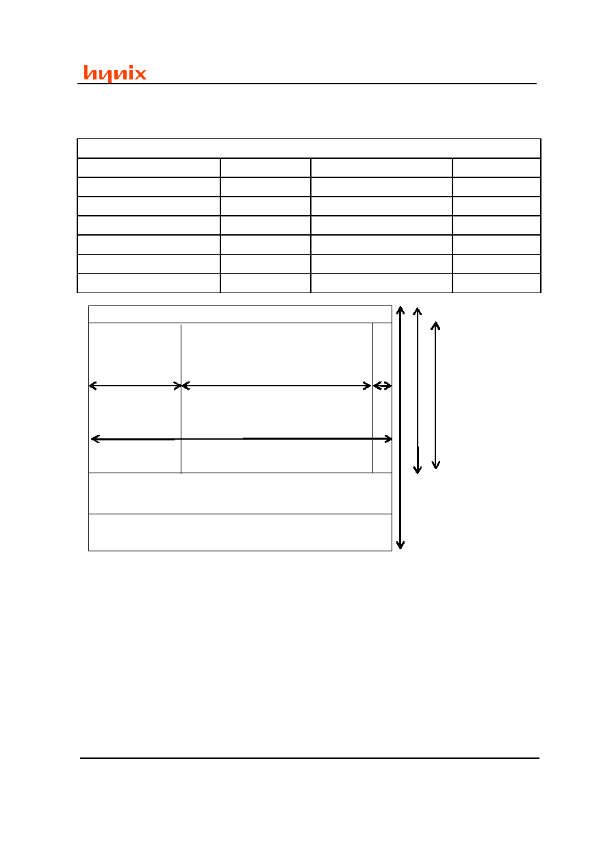
HV7151SP
CMOS Image Sensor
Confidential
With Image Signal Processing
This document is a general product description and is subject to change without notice. Hynix
Semiconductor Inc. does not assume any responsibility for use of circuits described and no patent
licenses are implied.
- 65 -
2003 Hynix Semiconductor Inc.
5. 5x5 Color Interpolation Timing (CifMode)
5x5 Color Interpolation Frame Timing Related Parameters
Master Clock Frequency(MCF)
19.2Mhz
PLL Out Clock Frequency(PCF)
MCF*2 = 38.4Mhz
Divided Clock Frequency(DCF)
PCF/1 = 38.4Mhz
Sensor Clock Frequency(SCF)
DCF/2 = 19.2Mhz
Sensor Clock Period(SCP)
1/19.2Mhz = 52ns
Window Width
352
Window Height
288
HBLANK Value
208
VBLANK Value
8
VSYNC Mode
Line Mode
Line Clock Period(LCP)
1366 SCPs
Output Bus Width
8bit
VGA Video Output Frequency
Irregular clock
Final Video Output Size
352x288
LCP(1366 SCPs)
ISP Dummy
(6 SCPs)
HSYNC (1152 SCPs)
Active Data: 352 EA
IDLE SLOT(4LCPs + (1024+HBLANK)*4)
HBLANK
(208 SCPs)
VBLANK[VSYNC]
(8 LCPs)
HOLD SLOT
(Integration Time Core Frame Time)
Real Frame
Time
Core Frame
Time
Video Lines is
active every
LCP, that is,
288 Video Lines
for 864 LCPs
If Integration Time < Core Frame Time, Real Frame Time is
4 * (208 + 1152+6) SCPs + 864 * (208 + 1152+6) SCPs + 8 * (208 + 1152+6) SCPs + 4 *
(208+1024)= 1201544 SCPs = 0.062580sec -> 15.979 frame per sec.
else Real Frame Time is
Integration Time * SCPs + 8 * (208 + 1152 + 6) SCPs.
HOLD SLOT in frame timing appears only if integration time is larger than core frame time.
QCifMode Frame rate is same as CifMode Frame rate.
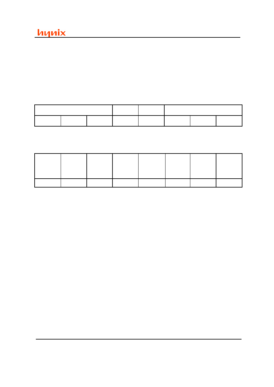
HV7151SP
CMOS Image Sensor
Confidential
With Image Signal Processing
This document is a general product description and is subject to change without notice. Hynix
Semiconductor Inc. does not assume any responsibility for use of circuits described and no patent
licenses are implied.
- 66 -
2003 Hynix Semiconductor Inc.
Output Data according to Video Mode
Output Data according to Video Mode is controlled by configuring Sensor Control A[01h] and Output
Format register[31h]. Configurable options are specified again for your reference.
Sensor Control A [SCTRA : 01h : 13h]
7
6
5
4
3
2
1
0
Reserved
X-Flip
Y-Flip
Video Mode
0
0
0
1
0
0
1
1
Output Format [OUTFMT : 31h : 31h]
7
6
5
4
3
2
1
0
Gamma-
Corrected
Bayer
Bayer 8bit
Output
Cb/B First
Y First
YCbCr
4:4:4 / 4:2:2
RGB
4:4:4
RGB 565
8 bit Output
0
0
1
1
0
0
0
1
Output timings for general configurations are described below. Slot named as "X" means that it is has
no meaningful value and should be discarded. 8bit Output is active, C[7:0] are always Hi-Z state. In
Case of Cb or Cr data, the digit stands for its sequence, respectively. For example, Cb01 is equal to
average of Cb0 and Cb1.
5X5 Mode or Sub-sampling(1/4, 1/16) Mode
1. YCbCr 4:2:2 with 8bit output
Register bit configurations
Sensor Control A : 5x5 Mode or Sub-sampling Mode
Output Format : 8bit Output, Y First, Cb/B First
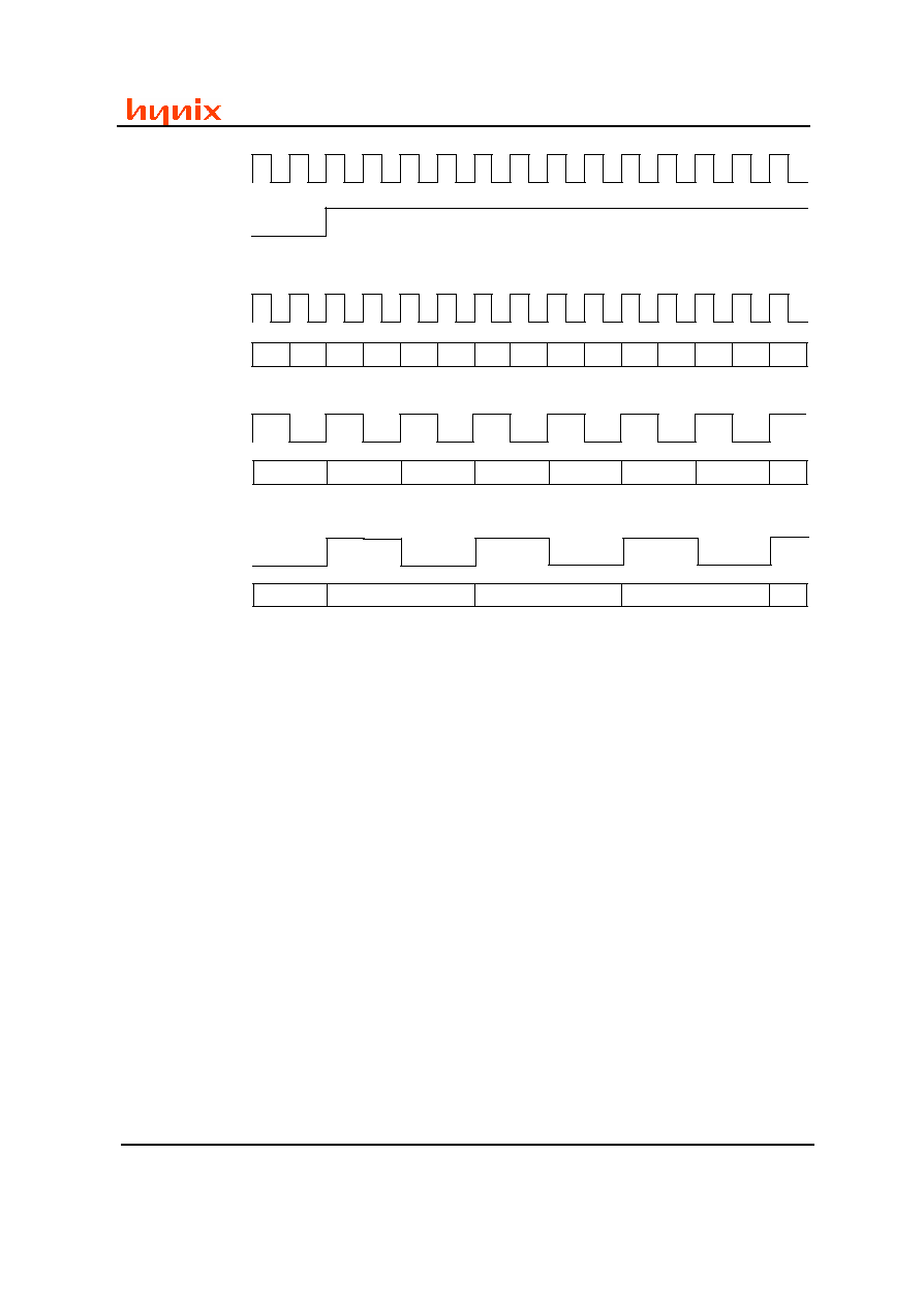
HV7151SP
CMOS Image Sensor
Confidential
With Image Signal Processing
This document is a general product description and is subject to change without notice. Hynix
Semiconductor Inc. does not assume any responsibility for use of circuits described and no patent
licenses are implied.
- 67 -
2003 Hynix Semiconductor Inc.
HSYNC
MCLK
Y6
Cr45
Y5
Cb45
Y4
Cr23
Y3
Cb23
Y2
Cr01
Y1
Cb01
Y0
X
X
Y6
Cr45
Y5
Cb45
Y4
Cr23
Y3
Cb23
Y2
Cr01
Y1
Cb01
Y0
X
X
Y6
Cb46
Y4
Cr02
Y2
Cb02
Y0
X
Y6
Cb46
Y4
Cr02
Y2
Cb02
Y0
X
Cr04
Y4
Cb04
Y0
X
Cr04
Y4
Cb04
Y0
X
1/4 Sub-sampling Video Clock & Output Data
5X5 Mode Video Clock & Output Data
CLK
Y[7:0]
CLK
Y[7:0]
1/16 Sub-sampling Video Clock & Output Data
CLK
Y[7:0]
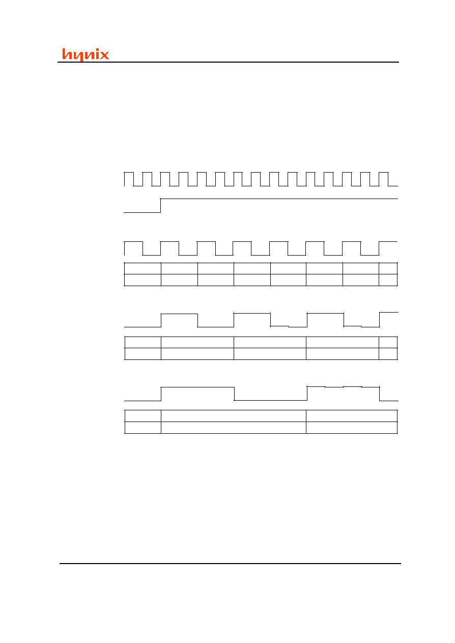
HV7151SP
CMOS Image Sensor
Confidential
With Image Signal Processing
This document is a general product description and is subject to change without notice. Hynix
Semiconductor Inc. does not assume any responsibility for use of circuits described and no patent
licenses are implied.
- 68 -
2003 Hynix Semiconductor Inc.
2. YCbCr 4:2:2 with 16bit output
Register bit configurations
Sensor Control A : 5x5 Mode or Sub-sampling Mode
Output Format : 16bit Output, Cb/B First
HSYNC
MCLK
Y6
Y4
Y2
Y0
X
Y6
Y4
Y2
Y0
X
1/4 Sub-sampling Video Clock & Output Data
5X5 Mode Video Clock & Output Data
Cr46
Cb46
Cr02
Cb02
X
Cr46
Cb46
Cr02
Cb02
X
Y6
Y5
Y4
Y3
Y2
Y1
Y0
X
Y6
Y5
Y4
Y3
Y2
Y1
Y0
X
Cb67
Cr45
Cb45
Cr23
Cb23
Cr01
Cb01
X
Cb67
Cr45
Cb45
Cr23
Cb23
Cr01
Cb01
X
Y4
Y0
X
Y4
Y0
X
Cr04
Cb04
X
Cr04
Cb04
X
CLK
Y[7:0]
C[7:0]
CLK
Y[7:0]
C[7:0]
1/16 Sub-sampling Video Clock & Output Data
CLK
Y[7:0]
C[7:0]
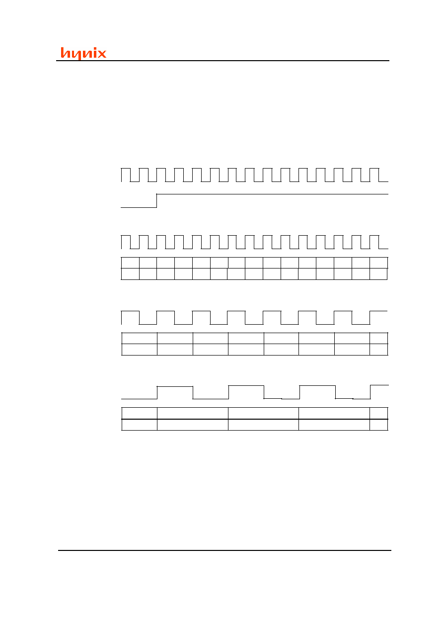
HV7151SP
CMOS Image Sensor
Confidential
With Image Signal Processing
This document is a general product description and is subject to change without notice. Hynix
Semiconductor Inc. does not assume any responsibility for use of circuits described and no patent
licenses are implied.
- 69 -
2003 Hynix Semiconductor Inc.
3. YCbCr 4:4:4 with 16bit output
Register bit configurations
Sensor Control A : 5x5 Mode or Sub-sampling Mode
Output Format : 16bit Output, Y First, Cb/B First
HSYNC
MCLK
Y6
X
Y5
X
Y4
X
Y3
X
Y2
X
Y1
X
Y0
X
X
Y6
X
Y5
X
Y4
X
Y3
X
Y2
X
Y1
X
Y0
X
X
Y6
X
Y4
X
Y2
X
Y0
X
Y6
X
Y4
X
Y2
X
Y0
X
X
Y4
X
Y0
X
X
Y4
X
Y0
X
1/4 Sub-sampling Video Clock & Output Data
5X5 Mode Video Clock & Output Data
CLK
CLK
1/16 Sub-sampling Video Clock & Output Data
CLK
Cb6
Cr5
Cb5
Cr4
Cb4
Cr3
Cb3
Cr2
Cb2
Cr1
Cb1
Cr0
Cb0
X
X
Cb6
Cr5
Cb5
Cr4
Cb4
Cr3
Cb3
Cr2
Cb2
Cr1
Cb1
Cr0
Cb0
X
X
Y[7:0]
C[7:0]
Cb6
Cr4
Cb4
Cr2
Cb2
Cr0
Cb0
X
Cb6
Cr4
Cb4
Cr2
Cb2
Cr0
Cb0
X
Y[7:0]
C[7:0]
Cr4
Cb4
Cr0
Cb0
X
Cr4
Cb4
Cr0
Cb0
X
Y[7:0]
C[7:0]
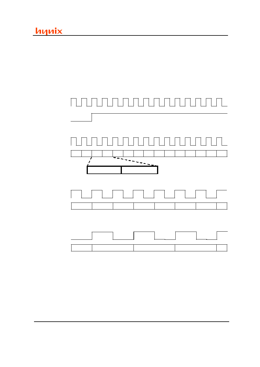
HV7151SP
CMOS Image Sensor
Confidential
With Image Signal Processing
This document is a general product description and is subject to change without notice. Hynix
Semiconductor Inc. does not assume any responsibility for use of circuits described and no patent
licenses are implied.
- 70 -
2003 Hynix Semiconductor Inc.
4. RGB 565 with 8bit output
Register bit configurations
Sensor Control A : 5x5 Mode or Sub-sampling Mode
Output Format : 8bit Output, Cb/B First, RGB565
HSYNC
MCLK
RG6
GB5
RG5
GB4
RG4
GB3
RG3
GB2
RG2
BG1
RG1
GB0
RG0
X
X
RG6
GB5
RG5
GB4
RG4
GB3
RG3
GB2
RG2
BG1
RG1
GB0
RG0
X
X
RG6
GB4
RG4
GB2
RG2
GB0
RG0
X
RG6
GB4
RG4
GB2
RG2
GB0
RG0
X
GB4
RG4
GB0
RG0
X
GB4
RG4
GB0
RG0
X
1/4 Sub-sampling Video Clock & Output Data
5X5 Mode Video Clock & Output Data
CLK
CLK
1/16 Sub-sampling Video Clock & Output Data
CLK
Y[7:0]
Y[7:0]
Y[7:0]
{G0[4:2]B0[7:3]}
{R0[7:3]G0[7:5]} {G0[4:2]B0[7:3]}
{R0[7:3]G0[7:5]}
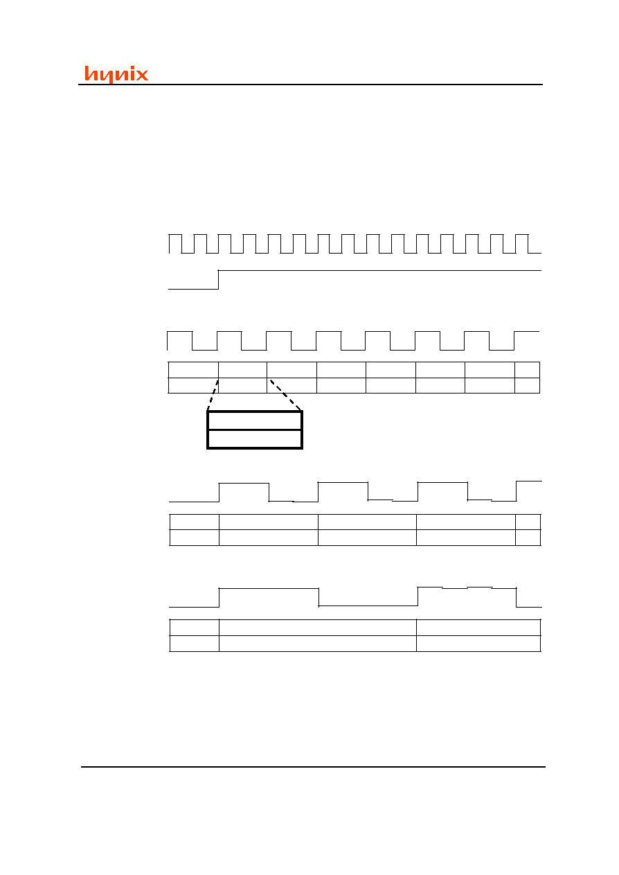
HV7151SP
CMOS Image Sensor
Confidential
With Image Signal Processing
This document is a general product description and is subject to change without notice. Hynix
Semiconductor Inc. does not assume any responsibility for use of circuits described and no patent
licenses are implied.
- 71 -
2003 Hynix Semiconductor Inc.
5. RGB 565 with 16bit output
Register bit configurations
Sensor Control A : 5x5 Mode or Sub-sampling Mode
Output Format : 16bit Output, Cb/B First, RGB565
HSYNC
MCLK
5X5 Mode Video Clock & Output Data
{R0[7:3]G0[7:5]}
{R0[7:3]G0[7:5]}
RG6
RG5
RG4
RG3
RG2
RG1
RG0
X
RG6
RG5
RG4
RG3
RG2
RG1
RG0
X
CLK
GB6
GB5
GB4
GB3
GB2
GB1
GB0
X
GB6
GB5
GB4
GB3
GB2
GB1
GB0
X
Y[7:0]
C[7:0]
{G0[4:2]B0[7:3]}
{G0[4:2]B0[7:3]}
RG6
RG4
RG2
RG0
X
RG6
RG4
RG2
RG0
X
1/4 Sub-sampling Video Clock & Output Data
GB6
GB4
GB2
GB0
X
GB6
GB4
GB2
GB0
X
RG4
RG0
X
RG4
RG0
X
GB4
GB0
X
GB4
GB0
X
CLK
Y[7:0]
C[7:0]
1/16 Sub-sampling Video Clock & Output Data
CLK
Y[7:0]
C[7:0]
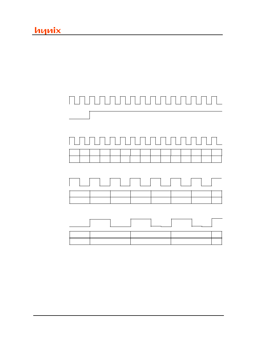
HV7151SP
CMOS Image Sensor
Confidential
With Image Signal Processing
This document is a general product description and is subject to change without notice. Hynix
Semiconductor Inc. does not assume any responsibility for use of circuits described and no patent
licenses are implied.
- 72 -
2003 Hynix Semiconductor Inc.
6. RGB 4:4:4 with 16bit output
Register bit configurations
Sensor Control A : 5x5 Mode or Sub-sampling Mode
Output Format : 16bit Output, Cb/B First, RGB4:4:4
HSYNC
MCLK
G6
X
G5
X
G4
X
G3
X
G2
X
G1
X
G0
X
X
G6
X
G5
X
G4
X
G3
X
G2
X
G1
X
G0
X
X
G6
X
G4
X
G2
X
G0
X
G6
X
G4
X
G2
X
G0
X
X
G4
X
G0
X
X
G4
X
G0
X
1/4 Sub-sampling Video Clock & Output Data
5X5 Mode Video Clock & Output Data
CLK
CLK
1/16 Sub-sampling Video Clock & Output Data
CLK
B6
R5
B5
R4
B4
R3
B3
R2
B2
R1
B1
R0
B0
X
X
B6
R5
B5
R4
B4
R3
B3
R2
B2
R1
B1
R0
B0
X
X
Y[7:0]
C[7:0]
B6
R4
B4
R2
B2
R0
B0
X
B6
R4
B4
R2
B2
R0
B0
X
Y[7:0]
C[7:0]
R4
B4
R0
B0
X
R4
B4
R0
B0
X
Y[7:0]
C[7:0]
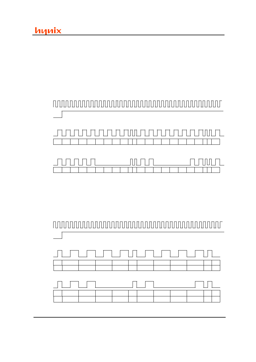
HV7151SP
CMOS Image Sensor
Confidential
With Image Signal Processing
This document is a general product description and is subject to change without notice. Hynix
Semiconductor Inc. does not assume any responsibility for use of circuits described and no patent
licenses are implied.
- 73 -
2003 Hynix Semiconductor Inc.
VGA Mode or QVGA Mode
1. YCbCr 4:2:2 with 8bit output
Register bit configurations
Sensor Control A : VGA Mode or QVGA Mode
Output Format : 8bit Output, Y First, Cb/B First
2. YCbCr 4:2:2 with 16bit output
Register bit configurations
Sensor Control A : VGA Mode or QVGA Mode
Output Format : 16bit Output, Cb/B First
HSYNC
MCLK
VGA Mode Video Clock & Output Data
CLK
Y[7:0]
QVGA Mode Video Clock & Output Data
Cr
89
Y9
Cb89
Y7
Cr67
Y8
Cb67
Y10
Y6
Cr45
Y5
Cb
45
Y4
Cr23
Y3
Cb23
Y2
Cr01
Y1
Cb01
Y0
X
Cr
89
Y9
Cb89
Y7
Cr67
Y8
Cb67
Y10
Y6
Cr45
Y5
Cb
45
Y4
Cr23
Y3
Cb23
Y2
Cr01
Y1
Cb01
Y0
X
Cr
89
Y9
Cb89
X
X
Y8
X
X
X
Cr45
Y5
Cb
45
Y4
X
X
X
X
Cr01
Y1
Cb01
Y0
X
Cr
89
Y9
Cb89
X
X
Y8
X
X
X
Cr45
Y5
Cb
45
Y4
X
X
X
X
Cr01
Y1
Cb01
Y0
X
CLK
Y[7:0]
HSYNC
MCLK
VGA Mode Video Clock & Output Data
CLK
Y[7:0]
C[7:0]
QVGA Mode Video Clock & Output Data
CLK
RG9
RG7
RG8
RG10
RG6
RG5
RG4
RG3
RG2
RG1
RG0
X
RG9
RG7
RG8
RG10
RG6
RG5
RG4
RG3
RG2
RG1
RG0
X
GB9
GB7
GB8
GB10
GB6
GB5
GB4
GB3
GB2
GB1
GB0
X
GB9
GB7
GB8
GB10
GB6
GB5
GB4
GB3
GB2
GB1
GB0
X
Y[7:0]
C[7:0]
Y9
X
Y8
Y10
X
Y5
Y4
X
X
Y1
Y0
X
Y9
X
Y8
Y10
X
Y5
Y4
X
X
Y1
Y0
X
Cr89
X
Cb89
X
Cr45
Cb45
X
X
Cr01
Cb01
X
Cr89
X
Cb89
X
Cr45
Cb45
X
X
Cr01
Cb01
X
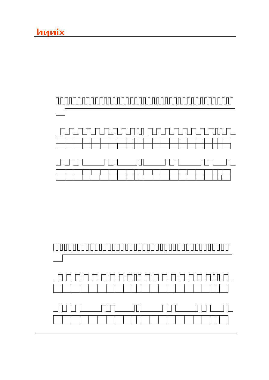
HV7151SP
CMOS Image Sensor
Confidential
With Image Signal Processing
This document is a general product description and is subject to change without notice. Hynix
Semiconductor Inc. does not assume any responsibility for use of circuits described and no patent
licenses are implied.
- 74 -
2003 Hynix Semiconductor Inc.
3. YCbCr 4:4:4 with 16bit output
Register bit configurations
Sensor Control A : VGA Mode or QVGA Mode
Output Format : 16bit Output, Y First, Cb/B First
4. RGB 565 with 8bit output
Register bit configurations
Sensor Control A : VGA Mode or QVGA Mode
Output Format : 8bit Output, Cb/B First, RGB565
HSYNC
MCLK
VGA Mode Video Clock & Output Data
CLK
Y[7:0]
C[7:0]
QVGA Mode Video Clock & Output Data
CLK
X
Y9
X
Y7
X
Y8
X
Y10
Y6
X
Y5
X
Y4
X
Y3
X
Y2
X
Y1
X
Y0
X
X
Y9
X
Y7
X
Y8
X
Y10
Y6
X
Y5
X
Y4
X
Y3
X
Y2
X
Y1
X
Y0
X
Cr9
Cb9
Cr8
Cb7
Cr7
Cb8
Cr6
Cb10
Cb6
Cr5
Cb5
Cr4
C
b4
Cr3
Cb3
Cr2
Cb2
Cr1
Cb1
Cr0
Cb0
X
Cr9
Cb9
Cr8
Cb7
Cr7
Cb8
Cr6
Cb10
Cb6
Cr5
Cb5
Cr4
C
b4
Cr3
Cb3
Cr2
Cb2
Cr1
Cb1
Cr0
Cb0
X
Y[7:0]
C[7:0]
X
X
X
X
X
Y8
X
Y10
Y6
X
X
X
Y4
X
X
X
Y2
X
X
X
Y0
X
X
X
X
X
X
Y8
X
Y10
Y6
X
X
X
Y4
X
X
X
Y2
X
X
X
Y0
X
X
X
Cr8
X
X
Cb8
Cr6
Cb10
Cb6
X
X
Cr4
C
b4
X
X
Cr2
Cb2
X
X
Cr0
Cb0
X
X
X
Cr8
X
X
Cb8
Cr6
Cb10
Cb6
X
X
Cr4
C
b4
X
X
Cr2
Cb2
X
X
Cr0
Cb0
X
HSYNC
MCLK
VGA Mode Video Clock & Output Data
CLK
Y[7:0]
QVGA Mode Video Clock & Output Data
CLK
GB
9
RG
9
GB8
RG7
GB7
RG8
GB6
RG10
RG6
GB5
RG5
GB
4
RG
4
GB3
RG3
GB2
RG2
GB1
RG1
GB0
RG0
X
GB
9
RG
9
GB8
RG7
GB7
RG8
GB6
RG10
RG6
GB5
RG5
GB
4
RG
4
GB3
RG3
GB2
RG2
GB1
RG1
GB0
RG0
X
Y[7:0]
X
X
GB8
X
X
RG8
GB6
RG10
RG6
X
X
GB
4
RG
4
X
X
GB2
RG2
X
X
GB0
RG0
X
X
X
GB8
X
X
RG8
GB6
RG10
RG6
X
X
GB
4
RG
4
X
X
GB2
RG2
X
X
GB0
RG0
X
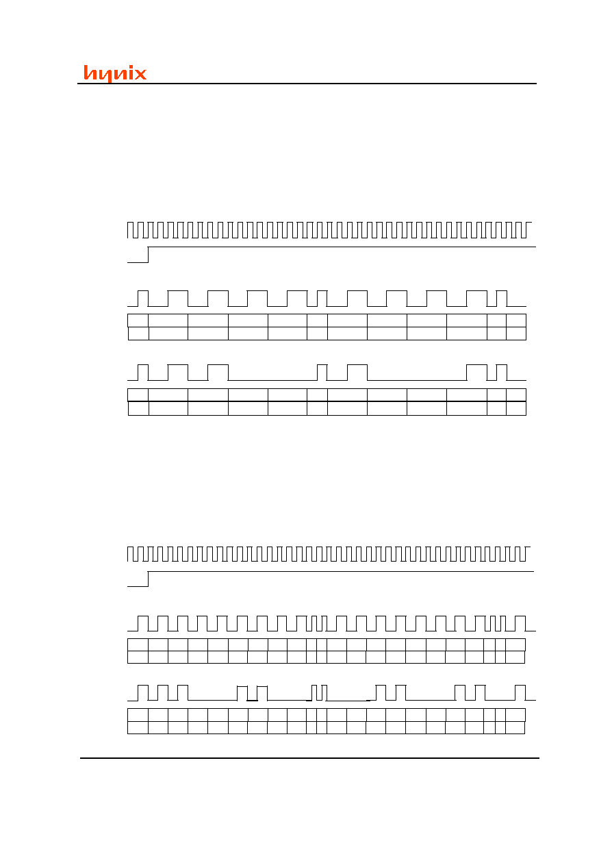
HV7151SP
CMOS Image Sensor
Confidential
With Image Signal Processing
This document is a general product description and is subject to change without notice. Hynix
Semiconductor Inc. does not assume any responsibility for use of circuits described and no patent
licenses are implied.
- 75 -
2003 Hynix Semiconductor Inc.
5. RGB 565 with 16bit output
Register bit configurations
Sensor Control A : VGA Mode or QVGA Mode
Output Format : 16bit Output, Cb/B First, RGB565
6. RGB 4:4:4 with 16bit output
Register bit configurations
Sensor Control A : VGA Mode or QVGA Mode
Output Format : 16bit Output, Cb/B First, RGB4:4:4
HSYNC
MCLK
VGA Mode Video Clock & Output Data
CLK
Y[7:0]
C[7:0]
QVGA Mode Video Clock & Output Data
CLK
RG9
RG7
RG8
RG10
RG6
RG5
RG4
RG3
RG2
RG1
RG0
X
RG9
RG7
RG8
RG10
RG6
RG5
RG4
RG3
RG2
RG1
RG0
X
GB9
GB7
GB8
GB10
GB6
GB5
GB4
GB3
GB2
GB1
GB0
X
GB9
GB7
GB8
GB10
GB6
GB5
GB4
GB3
GB2
GB1
GB0
X
Y[7:0]
C[7:0]
RG9
X
RG8
X
X
RG5
RG4
X
X
RG1
RG0
X
RG9
X
RG8
X
X
RG5
RG4
X
X
RG1
RG0
X
GB9
X
GB8
X
X
GB5
GB4
X
X
GB1
GB0
X
GB9
X
GB8
X
X
GB5
GB4
X
X
GB1
GB0
X
HSYNC
MCLK
VGA Mode Video Clock & Output Data
CLK
Y[7:0]
C[7:0]
QVGA Mode Video Clock & Output Data
CLK
X
G9
X
G7
X
G8
X
G10
G6
X
G5
X
G4
X
G3
X
G2
X
G1
X
G0
X
X
G9
X
G7
X
G8
X
G10
G6
X
G5
X
G4
X
G3
X
G2
X
G1
X
G0
X
R9
B9
R8
B7
R7
B8
R6
B10
B6
R5
B5
R4
B4
R3
B3
R2
B2
R1
B1
R0
B0
X
R9
B9
R8
B7
R7
B8
R6
B10
B6
R5
B5
R4
B4
R3
B3
R2
B2
R1
B1
R0
B0
X
Y[7:0]
C[7:0]
X
X
X
X
X
G8
X
G10
G6
X
X
X
G4
X
X
X
G2
X
X
X
G0
X
X
X
X
X
X
G8
X
G10
G6
X
X
X
G4
X
X
X
G2
X
X
X
G0
X
X
X
R8
X
X
B8
R6
B10
B6
X
X
R4
B4
X
X
R2
B2
X
X
R0
B0
X
X
X
R8
X
X
B8
R6
B10
B6
X
X
R4
B4
X
X
R2
B2
X
X
R0
B0
X
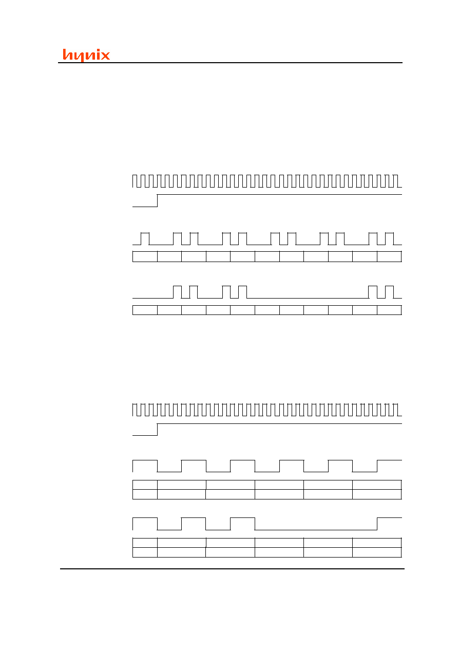
HV7151SP
CMOS Image Sensor
Confidential
With Image Signal Processing
This document is a general product description and is subject to change without notice. Hynix
Semiconductor Inc. does not assume any responsibility for use of circuits described and no patent
licenses are implied.
- 76 -
2003 Hynix Semiconductor Inc.
CIF Mode or QCIF Mode
1. YCbCr 4:2:2 with 8bit output
Register bit configurations
Sensor Control A : CIF Mode or QCIF Mode
Output Format : 8bit Output, Y First, Cb/B First
2. YCbCr 4:2:2 with 16bit output
Register bit configurations
Sensor Control A : CIF Mode or QCIF Mode
Output Format : 16bit Output, Cb/B First
HSYNC
Cb45
Y4
Cr23
Y3
Cb23
Y2
Cr01
Y1
Cb01
Y0
X
Cb45
Y4
Cr23
Y3
Cb23
Y2
Cr01
Y1
Cb01
Y0
X
MCLK
Cb01
Y4
X
X
X
X
Cr01
Y1
Cb01
Y0
X
Cb01
Y4
X
X
X
X
Cr01
Y1
Cb01
Y0
X
CIF Mode Video Clock & Output Data
QCIF Mode Video Clock & Output Data
CLK
Y[7:0]
CLK
Y[7:0]
HSYNC
Y4
Y3
Y2
Y1
Y0
X
Y4
Y3
Y2
Y1
Y0
X
MCLK
Y4
X
X
Y1
Y0
X
Y4
X
X
Y1
Y0
X
CIF Mode Video Clock & Output Data
QCIF Mode Video Clock & Output Data
CLK
Y[7:0]
C[7:0]
CLK
Y[7:0]
C[7:0]
Cb45
Cr23
Cb23
Cr01
Cb01
X
Cb45
Cr23
Cb23
Cr01
Cb01
X
Cb45
X
X
Cr01
Cb01
X
Cb45
X
X
Cr01
Cb01
X
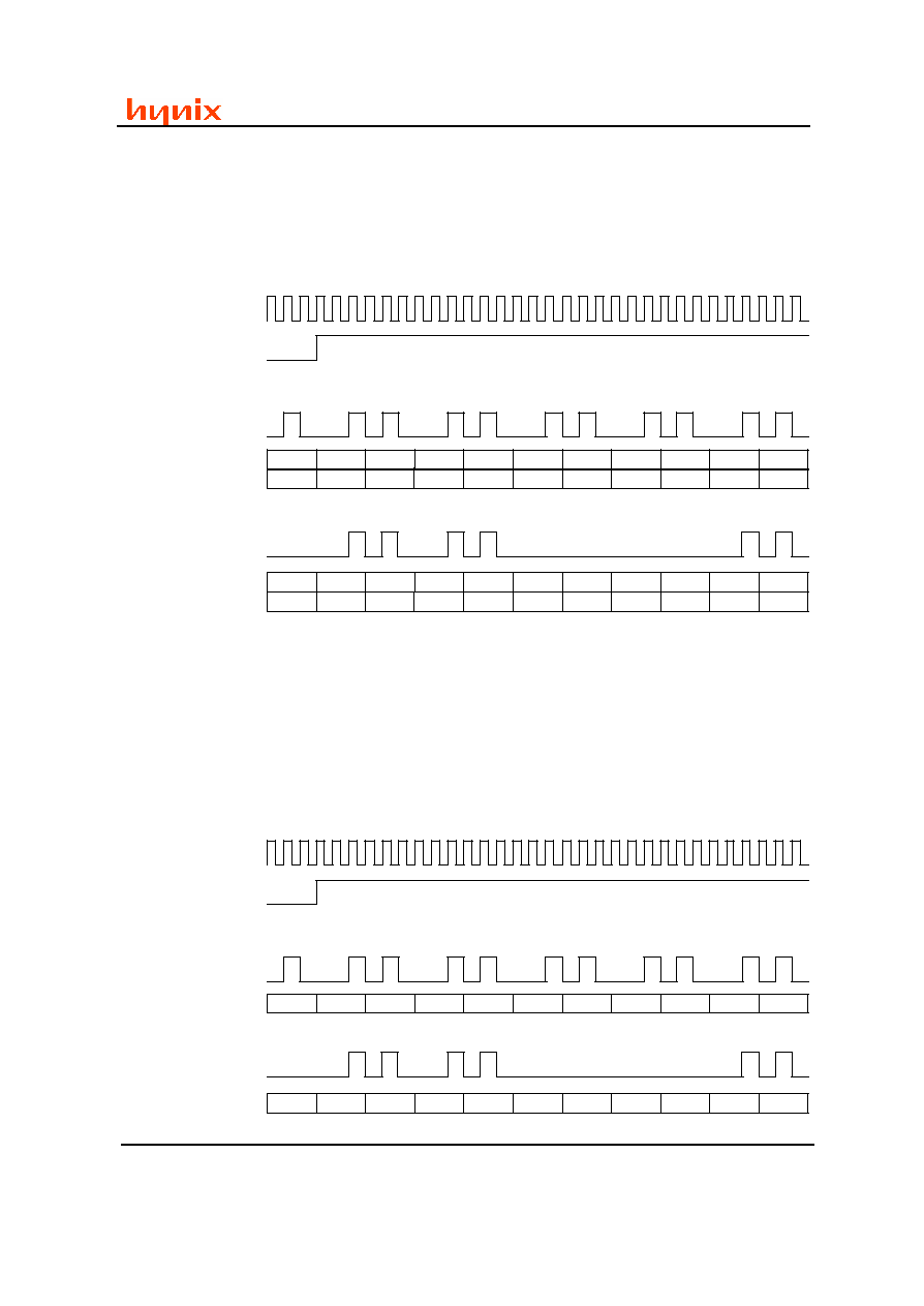
HV7151SP
CMOS Image Sensor
Confidential
With Image Signal Processing
This document is a general product description and is subject to change without notice. Hynix
Semiconductor Inc. does not assume any responsibility for use of circuits described and no patent
licenses are implied.
- 77 -
2003 Hynix Semiconductor Inc.
3. YCbCr 4:4:4 with 16bit output
Register bit configurations
Sensor Control A : CIF Mode or QCIF Mode
Output Format : 16bit Output, Y First, Cb/B First
4. RGB 565 with 8bit output
Register bit configurations
Sensor Control A : CIF Mode or QCIF Mode
Output Format : 8bit Output, Cb/B First, RGB565
HSYNC
MCLK
X
Y4
X
Y3
X
Y2
X
Y1
X
Y0
X
X
Y4
X
Y3
X
Y2
X
Y1
X
Y0
X
X
Y4
X
X
X
X
X
Y1
X
Y0
X
X
Y4
X
X
X
X
X
Y1
X
Y0
X
CIF Mode Video Clock & Output Data
QCIF Mode Video Clock & Output Data
CLK
Y[7:0]
C[7:0]
CLK
Y[7:0]
C[7:0]
Cr4
Cb4
Cr3
Cb3
Cr2
Cb2
Cr1
Cb1
Cr0
Cb0
X
Cr4
Cb4
Cr3
Cb3
Cr2
Cb2
Cr1
Cb1
Cr0
Cb0
X
Cr4
Cb4
X
X
X
X
Cb1
Cb1
Cr0
Cb0
X
Cr4
Cb4
X
X
X
X
Cb1
Cb1
Cr0
Cb0
X
HSYNC
MCLK
GB4
RG4
GB3
RG3
GB2
RG2
GB1
RG1
GB0
RG0
X
GB4
RG4
GB3
RG3
GB2
RG2
GB1
RG1
GB0
RG0
X
GB4
RG4
X
X
X
X
GB1
RG1
GB0
RG0
X
GB4
RG4
X
X
X
X
GB1
RG1
GB0
RG0
X
CIF Mode Video Clock & Output Data
QCIF Mode Video Clock & Output Data
CLK
Y[7:0]
CLK
Y[7:0]
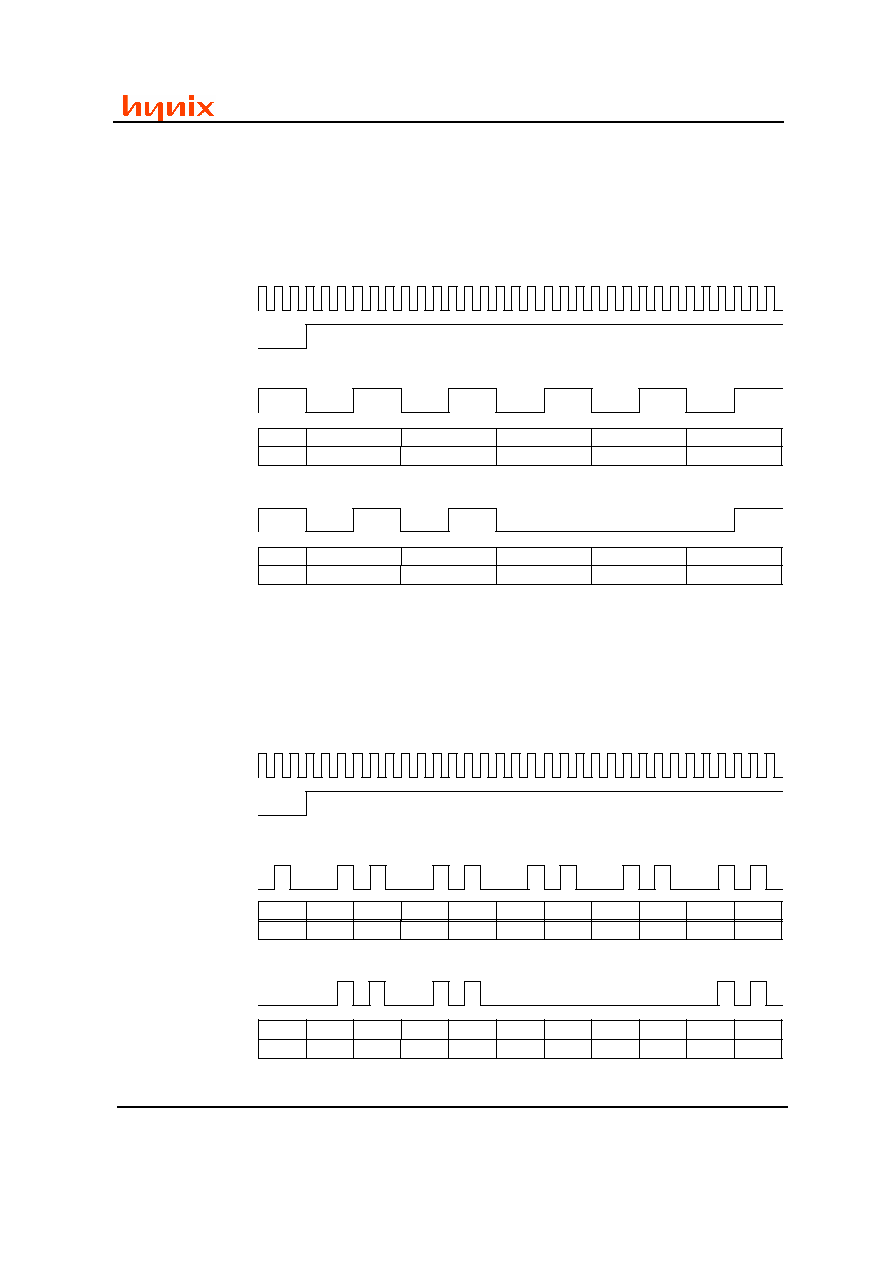
HV7151SP
CMOS Image Sensor
Confidential
With Image Signal Processing
This document is a general product description and is subject to change without notice. Hynix
Semiconductor Inc. does not assume any responsibility for use of circuits described and no patent
licenses are implied.
- 78 -
2003 Hynix Semiconductor Inc.
5. RGB 565 with 16bit output
Register bit configurations
Sensor Control A : CIF Mode or QCIF Mode
Output Format : 16bit Output, Cb/B First, RGB565
6. RGB 4:4:4 with 16bit output
Register bit configurations
Sensor Control A : CIF Mode or QCIF Mode
Output Format : 16bit Output, Cb/B First, RGB4:4:4
RG4
RG3
RG2
RG1
RG0
X
RG4
RG3
RG2
RG1
RG0
X
RG4
X
X
RG1
RG0
X
RG4
X
X
RG1
RG0
X
CIF Mode Video Clock & Output Data
QCIF Mode Video Clock & Output Data
CLK
Y[7:0]
C[7:0]
CLK
Y[7:0]
C[7:0]
GB4
GB3
GB2
GB1
GB0
X
GB4
GB3
GB2
GB1
GB0
X
GB4
X
X
GB1
GB0
X
GB4
X
X
GB1
GB0
X
HSYNC
MCLK
HSYNC
MCLK
X
G4
X
G3
X
G2
X
G1
X
G0
X
X
G4
X
G3
X
G2
X
G1
X
G0
X
X
G4
X
X
X
X
X
G1
X
G0
X
X
G4
X
X
X
X
X
G1
X
G0
X
CIF Mode Video Clock & Output Data
QCIF Mode Video Clock & Output Data
CLK
Y[7:0]
C[7:0]
CLK
Y[7:0]
C[7:0]
R4
B4
R3
B3
R2
B2
R1
B1
R0
B0
X
R4
B4
R3
B3
R2
B2
R1
B1
R0
B0
X
R4
B4
X
X
X
X
R1
B1
R0
B0
X
R4
B4
X
X
X
X
R1
B1
R0
B0
X
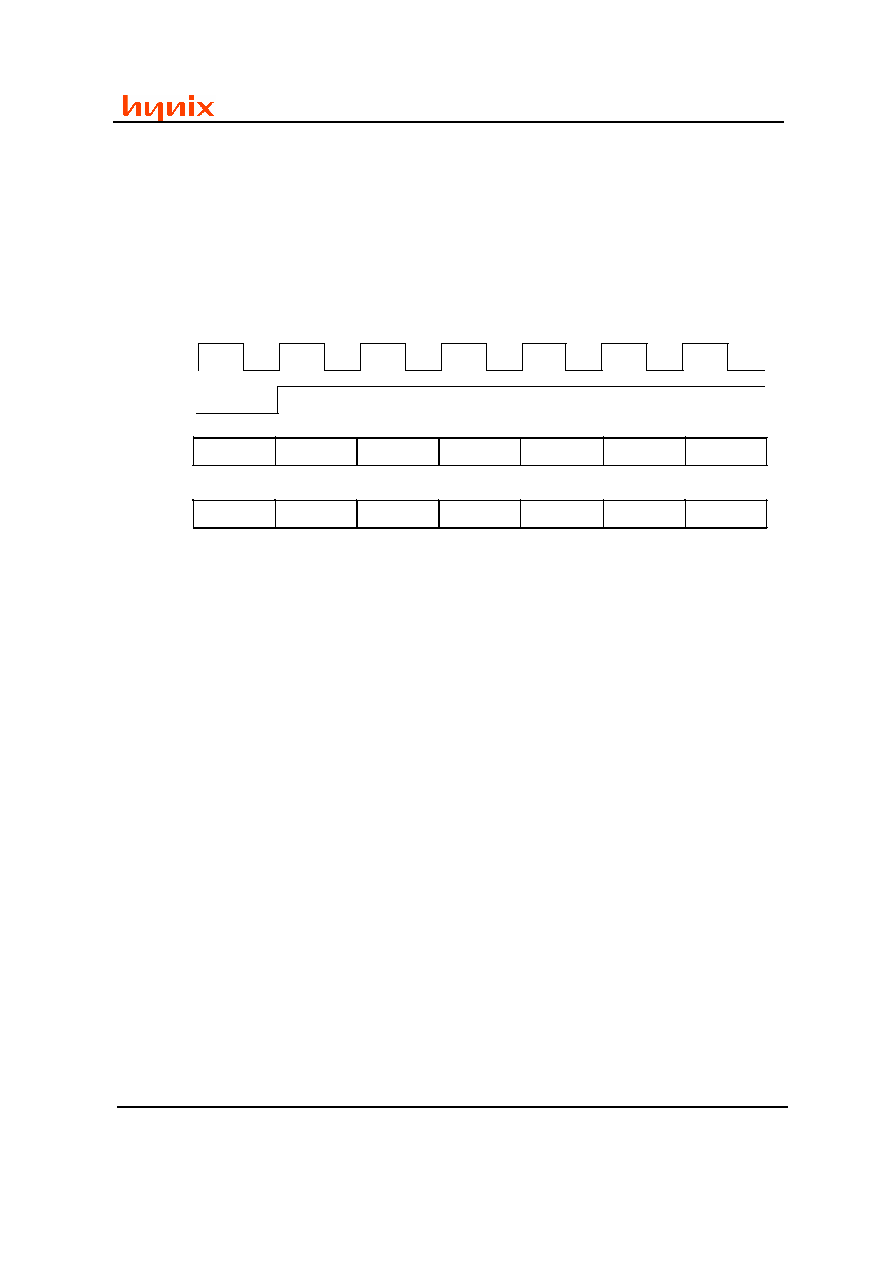
HV7151SP
CMOS Image Sensor
Confidential
With Image Signal Processing
This document is a general product description and is subject to change without notice. Hynix
Semiconductor Inc. does not assume any responsibility for use of circuits described and no patent
licenses are implied.
- 79 -
2003 Hynix Semiconductor Inc.
Bayer Data Format
SCTRA[2:0] is set to Bayer mode
- When Bayer output mode is selected, Window Width x Window Height raw image data are produced
with the following sequence. After VSYNC goes low state, the first HSYNC line of a frame is activated
with B pixel data appearing first when both of Column Start Address and Row Start Address are even.
Y[7:0]
Even Line
VCLK
Y[7:0]
Odd Line
HSYNC
X
B
G
B
G
B
G
X
G
R
G
R
G
R
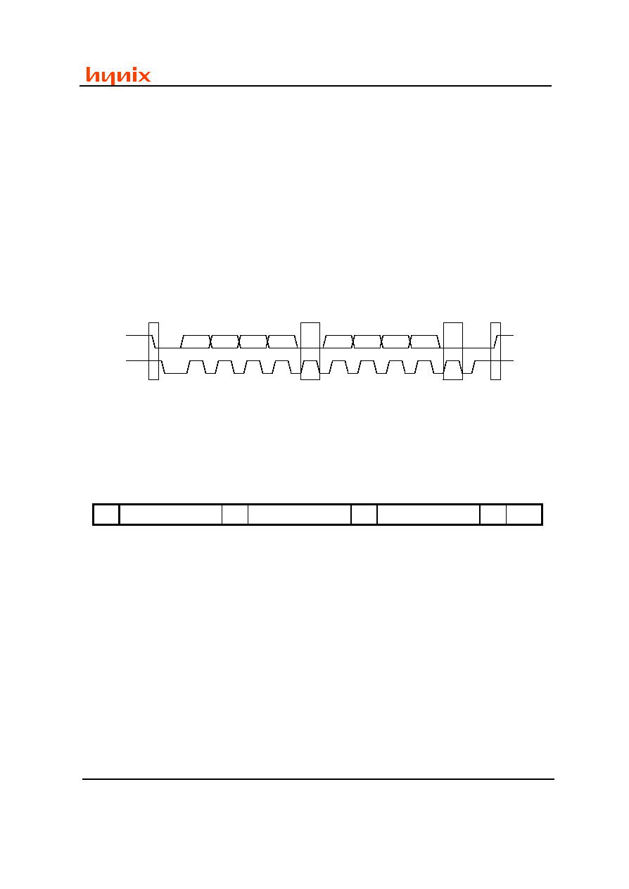
HV7151SP
CMOS Image Sensor
Confidential
With Image Signal Processing
This document is a general product description and is subject to change without notice. Hynix
Semiconductor Inc. does not assume any responsibility for use of circuits described and no patent
licenses are implied.
- 80 -
2003 Hynix Semiconductor Inc.
I2C Chip Interface
The serial bus interface consists of the SDA(serial data) and SCK(serial clock) pins. HV7151SP
sensor can operate only as a slave. The SCK only controls the serial interface. However, MCLK
should be supplied and RESET should be high signal during controlling the serial interface. The Start
condition is that logic transition (High to Low) on the SDA pin while the SCK pin is at high state. The
Stop condition is that logic transition (Low to High) on the SDA pin while the SCK pin is at high state.
To generate Acknowledge signal, the Sensor drives the SDA low when the SCK pin is at high state.
Every byte consists of 8 bits. Each byte transferred on the bus must be followed by an Acknowledge.
The most significant bit of the byte should always be transmitted first.
Register Write Sequences
One Byte Write
S
22H
A
01H
A
04H
A
P
*1
*2
*3
*4
*5
*6
*7
*8
Set "Sensor Control A" register into Window mode
*1. Drive: I2C start condition
*2. Drive: 22H(001_0001 + 0) [device address + R/W bit]
*3. Read: acknowledge from sensor
*4. Drive: 01H [sub-address]
*5. Read: acknowledge from sensor
*6. Drive: 04H [Video Mode : VGA]
*7. Read: acknowledge from sensor
*8. Drive: I2C stop condition
1
2
8
9
ACK
MSB
LSB
SDA
SCK
START
1
2
8
9
ACK
STOP
HV7151SP
CMOS Image Sensor
Confidential
With Image Signal Processing
This document is a general product description and is subject to change without notice. Hynix
Semiconductor Inc. does not assume any responsibility for use of circuits described and no patent
licenses are implied.
- 81 -
2003 Hynix Semiconductor Inc.
Multiple Byte Write using Auto Address Increment
S
22H
A
0cH
A
03H
A
60H
A
P
*1
*2
*3
*4
*5
*6
*7
*8
*9 *10
Set "AE Integration Step High/Low" register as 5161H with auto address increment
*1. Drive: I2C start condition
*2. Drive: 22H(001_0001 + 0) [device address + R/W bit]
*3. Read: acknowledge from sensor
*4. Drive: 0cH [sub-address]
*5. Read: acknowledge from sensor
*6. Drive: 03H [Window Height Upper]
*7. Read: acknowledge from sensor
*8. Drive: 60H [Window Height Lower]
*9. Read: acknowledge from sensor
*10. Drive: I2C stop condition
Register Read Sequence
S
22H
A
1cH
A S
23H
A
Data of 07H
A P
*1
*2
*3
*4
*5 *6
*7
*8
*9
*10 *11
Read "Reset Level Clamp" register from HV7151SP
*1. Drive: I2C start condition
*2. Drive: 22H(001_0001 + 0) [device address + R/W bit(be careful. R/W=0)]
*3. Read: acknowledge from sensor
*4. Drive: 1cH [sub-address]
*5. Read: acknowledge from sensor
*6. Drive: I
2
C start condition
*7. Drive: 23H(001_0001 + 1) [device address + R/W bit(be careful. R/W=1)]
*8. Read: acknowledge from sensor
*9. Read: Read "Reset Level Clamp" from sensor
*10. Drive: acknowledge to sensor. If there is more data bytes to read, SDA should be driven to low
and data read states(*9, *10) is repeated. Otherwise SDA should be driven to high to
prepare for the read transaction end.
*11. Drive: I2C stop condition
HV7151SP
CMOS Image Sensor
Confidential
With Image Signal Processing
This document is a general product description and is subject to change without notice. Hynix
Semiconductor Inc. does not assume any responsibility for use of circuits described and no patent
licenses are implied.
- 82 -
2003 Hynix Semiconductor Inc.
AC/DC Characteristics
Absolute Maximum Ratings
Symbol
Parameter
Units
Min.
Max.
Viopp
I/O block supply voltage
Volts
-0.3
3.3
Vdpp
Internal digital supply voltage
Volts
-0.3
2.5
Vapp
Analog supply voltage
Volts
-0.3
2.5
Vipp
Input signal voltage
Volts
-0.3
3.3
Top
Operating Temperature
°
C
-10
50
Tst
Storage Temperature
°
C
-30
80
Caution: Stresses exceeding the absolute maximum ratings may induce failure.
DC Operating Conditions
Symbol
Parameter
Units
Min.
Max.
Load[pF]
Notes
Vio
I/O block supply voltage
Volt
2.3
2.8
V
dd
Internal operation supply voltage
Volt
1.6
2.0
V
ih
Input voltage logic "1"
Volt
2.3
2.5
6.5
V
il
Input voltage logic "0"
Volt
0
0.8
6.5
V
oh
Output voltage logic "1"
Volt
2.15
Vio
60
V
ol
Output voltage logic "0"
Volt
0.4
60
I
oh
Output High Current
mA
-4
60
I
ol
Output Low Current
mA
4
60
T
a
Ambient operating temperature
Celsius
-10
50
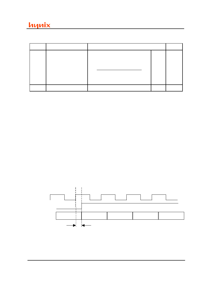
HV7151SP
CMOS Image Sensor
Confidential
With Image Signal Processing
This document is a general product description and is subject to change without notice. Hynix
Semiconductor Inc. does not assume any responsibility for use of circuits described and no patent
licenses are implied.
- 83 -
2003 Hynix Semiconductor Inc.
AC Operating Conditions
Symbol
Parameter
Max Operation Frequency
Units
Notes
MCLK
Main clock frequency
1) PLL off : 38.4
2) PLL on :
)
(
)
(Re
4
.
38
Divisor
Feedback
Divisor
ference
MHz
1,2,3
SCK
I
2
C clock frequency
400
KHz
4
1. MCLK may be divided by internal clock division logic for easy integration with high speed video
codec system.
2. Reference Divider and Feedback Divider is registers a3h and a4h, a5h, respectively.
3. Frame Rate : 15 frames/sec at 38.4Mhz and PLL off , HBLANK = 208, VBLANK = 8
4. SCK is driven by host processor. For the detail serial bus timing, refer to I2C chip interface
section
Output AC Characteristics
All output timing delays are measured with output load 60[pF]. Output delay includes the internal
clock path delay and output driving delay that changes in respect to the output load, the operating
environment, and a board design. Due to the variable valid time delay of the output, video output
signals Y[7:0], C[7:0], HSYNC, and VSYNC may be latched in the negative edge of VCLK for the
stable data transfer between the image sensor and video codec.
Y/C[7:0]
V C L K
X
Data 0
Data 1
Data 2
HSYNC
Data 3
3ns
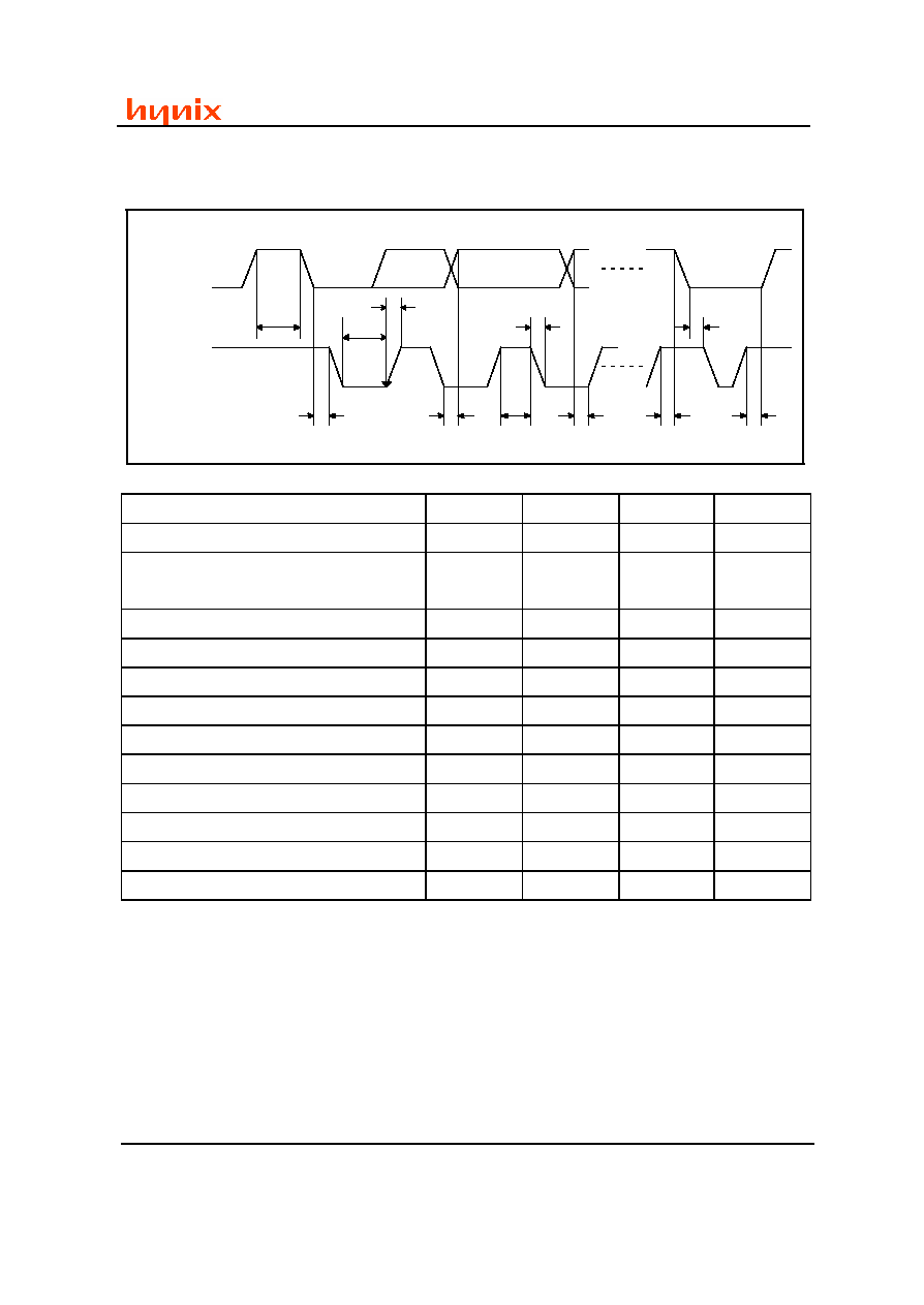
HV7151SP
CMOS Image Sensor
Confidential
With Image Signal Processing
This document is a general product description and is subject to change without notice. Hynix
Semiconductor Inc. does not assume any responsibility for use of circuits described and no patent
licenses are implied.
- 84 -
2003 Hynix Semiconductor Inc.
I2C Bus Timing
S D A
S C K
s t o p
s t a r t
t b u f
t l o w
tr
t h d ; s t a
t h d ; d a t
t h i g h
t s u ; d a t
t s u ; s t a
t s u ; s t o
s t o p
s t a r t
tf
t h d ; s t a
Parameter
Symbol
Min.
Max.
Unit
SCK clock frequency
f
sck
0
400
KHz
Time that I
2
C bus must be free before a
new transmission can start
t
buf
1.2
-
us
Hold time for a START
t
hd
;s
ta
1.0
-
us
LOW period of SCK
t
low
1.2
-
us
HIGH period of SCK
t
high
1.0
-
us
Setup time for START
t
su
;s
ta
1.2
-
us
Data hold time
t
hd
;d
at
0.1
-
us
Data setup time
t
su
;d
at
250
-
ns
Rise time of both SDA and SCK
t
r
-
250
ns
Fall time of both SDA and SCK
t
f
-
300
ns
Setup time for STOP
t
su
;s
to
1.2
-
us
Capacitive load of SCK/SDA
C
b
-
-
pf
HV7151SP
CMOS Image Sensor
Confidential
With Image Signal Processing
This document is a general product description and is subject to change without notice. Hynix
Semiconductor Inc. does not assume any responsibility for use of circuits described and no patent
licenses are implied.
- 85 -
2003 Hynix Semiconductor Inc.
Electro-Optical Characteristics
Parameter
Units
Min.
Typical
Max.
Target
Sensitivity
mV / lux
z
sec
1175
2200
Dark Signal
mV/ sec
TBD
Under 1
Dark Shading
mV/sec
TBD
Output Signal Shading
%
TBD
Output Saturation Signal
mV
610
600
Power Consumption (Normal Mode)
mW
60
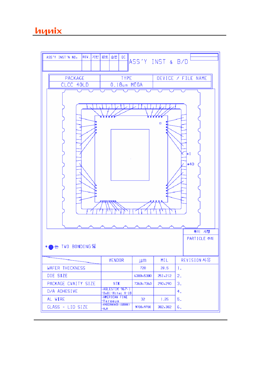
HV7151SP
CMOS Image Sensor
Confidential
With Image Signal Processing
This document is a general product description and is subject to change without notice. Hynix
Semiconductor Inc. does not assume any responsibility for use of circuits described and no patent
licenses are implied.
- 86 -
2003 Hynix Semiconductor Inc.
Package information
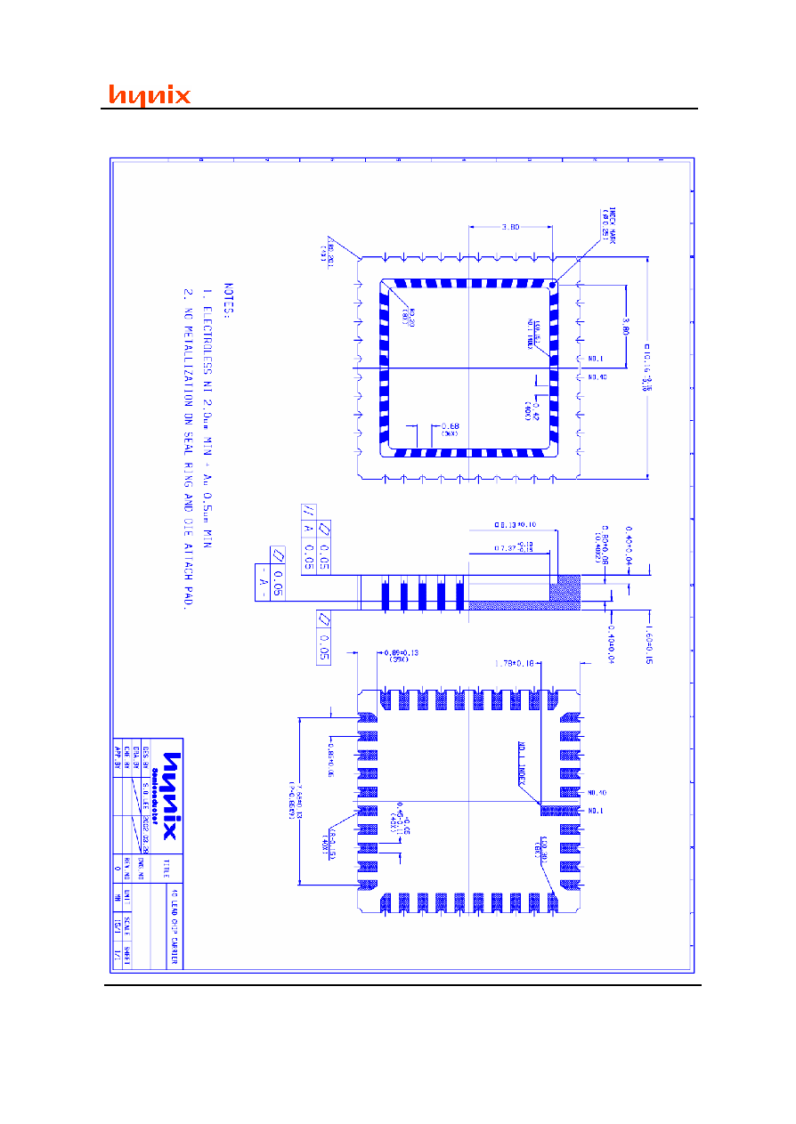
HV7151SP
CMOS Image Sensor
Confidential
With Image Signal Processing
This document is a general product description and is subject to change without notice. Hynix
Semiconductor Inc. does not assume any responsibility for use of circuits described and no patent
licenses are implied.
- 87 -
2003 Hynix Semiconductor Inc.
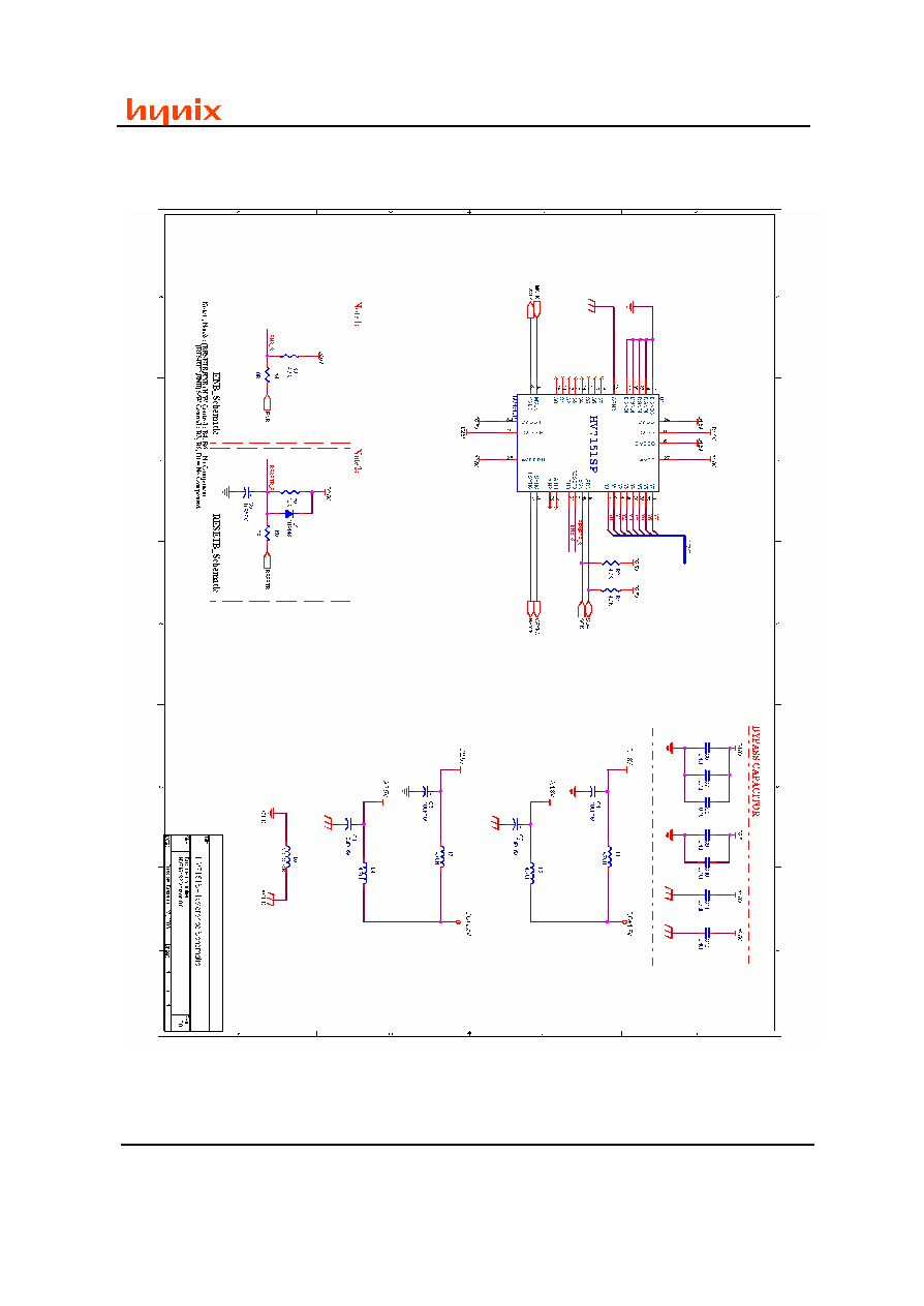
HV7151SP
CMOS Image Sensor
Confidential
With Image Signal Processing
This document is a general product description and is subject to change without notice. Hynix
Semiconductor Inc. does not assume any responsibility for use of circuits described and no patent
licenses are implied.
- 88 -
2003 Hynix Semiconductor Inc.
Reference Circuit Information

HV7151SP
CMOS Image Sensor
Confidential
With Image Signal Processing
This document is a general product description and is subject to change without notice. Hynix
Semiconductor Inc. does not assume any responsibility for use of circuits described and no patent
licenses are implied.
- 89 -
2003 Hynix Semiconductor Inc.
MEMO
Hynix Semiconductor Inc.
System IC SBU
* Contact Point *
MT Marketing Team
15Floor, Hynix Youngdong Bldg. 891 Daechi-Dong Kangnam-Gu Seoul 135-738 Republic of Korea
Tel: 82-2-3459-5579
Fax: 82-2-3459-5580
E-mail :
suyeon.moon@hynix.com