HI-SINCERITY
MICROELECTRONICS CORP.
Spec. No. : Preliminary Data
Issued Date : 2000.12.01
Revised Date : 2001.01.01
Page No. : 1/3
HSMC Product Specification
HM772A
PNP EPITAXIAL PLANAR TRANSISTOR
Description
The HM772A is designed for use in output stage of amplifier, voltage
regulator, DC-DC converter and driver.
Absolute Maximum Ratings
·
Maximum Temperatures
Storage Temperature ....................................................................................................... -55 ~ +150
°
C
Junction Temperature ............................................................................................... +150
°
C Maximum
·
Maximum Power Dissipation
Total Power Dissipation (Ta=25
°
C) ........................................................................................1 W
(Note1)
Total Power Dissipation (Ta=25
°
C)........................................................................................ 2 W
(Note2)
Total Power Dissipation (Ta=25
°
C)..................................................................................... 1.5 W
(Note3)
·
Maximum Voltages and Currents (Ta=25
°
C)
VCBO Collector to Base Voltage.................................................................................................... -60 V
VCEO Collector to Emitter Voltage................................................................................................. -50 V
VEBO Emitter to Base Voltage......................................................................................................... -5 V
IC Collector Current (continuous)..................................................................................................... -3 A
IC Collector Current (pulse) ................................................................................................. -7 A
(Note4)
Note1: When tested in free air condition, without heat sinking.
Note2: When mounted on a 40X40X1mm ceramic board.
Note3: Printed circuit board 2mm thick, collector plating 1cm square or larger.
Note4: Single pulse PW=1ms
Characteristics
(Ta=25
°
C)
Symbol
Min.
Typ.
Max.
Unit
Test Conditions
BVCBO
-60
-
-
V
IC=-100uA
BVCEO
-50
-
-
V
IC=-1mA
BVEBO
-5
-
-
V
IE=-10uA
ICBO
-
-
-1
uA
VCB=-30V
IEBO
-
-
-1
uA
VEB=-3V
*VCE(sat)
-
-0.3
-0.5
V
IC=-2A, IB=-0.2A
*VBE(sat)
-
-1
-2
V
IC=-2A, IB=-0.2A
*hFE1
30
-
-
VCE=-2V, IC=-20mA
*hFE2
100
160
500
VCE=-2V, IC=-1A
fT
-
80
-
MHz
VCE=-5V, IC=-100mA, f=100MHz
Cob
-
55
-
pF
VCB=-10V, f=1MHz
*Pulse Test : Pulse Width
380us, Duty Cycle
2%
Classification Of hFE2
Rank
Q
P
E
Range
100-200
160-320
250-500
HI-SINCERITY
MICROELECTRONICS CORP.
Spec. No. : Preliminary Data
Issued Date : 2000.12.01
Revised Date : 2001.01.01
Page No. : 2/3
HSMC Product Specification
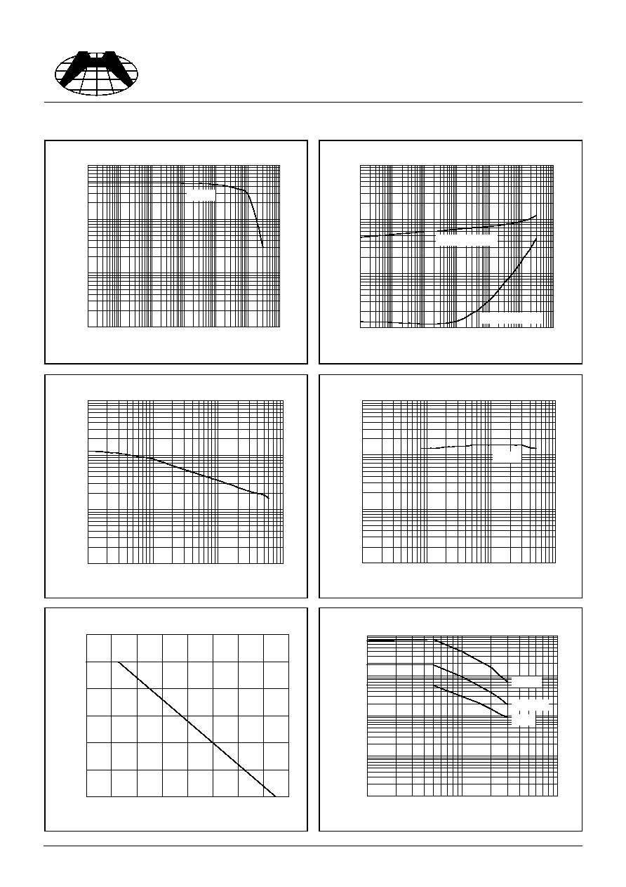
Characteristics Curve
Current Gain & Collector Current
1
10
100
1000
0.01
0.1
1
10
100
1000
10000
Collector Current (mA)
hF
E
V
CE
=2V
Saturation Voltage & Collector Current
0.01
0.1
1
10
0.01
0.1
1
10
100
1000
10000
Collector Current (mA)
S
a
tu
r
a
ti
o
n
V
o
l
t
a
g
e
(
V
)
V
BE(sat)
@ I
C
=10I
B
V
CE(sat)
@ I
C
=10I
B
Capacitance & Reverse-Biased Voltage
1
10
100
1000
0.1
1
10
100
Reverse-Biased Voltage (V)
Ca
p
a
c
i
t
a
n
c
e
(
p
F
)
Cob
Cutoff Frequency & Collector Current
1
10
100
1000
1
10
100
1000
Collector Current (mA)
C
u
to
ff F
r
e
q
u
e
n
c
y
(
M
H
z
)
V
CE
=5V
Safe Operating Area
1
10
100
1000
10000
1
10
100
Forward Biased Voltage-V
CE
(V)
C
o
l
l
e
c
t
o
r
C
u
rre
n
t
-I
C
(m
A
)
P
T
=1ms
P
T
=100ms
P
T
=1s
Power Derating
0
200
400
600
800
1000
1200
0
20
40
60
80
100
120
140
160
Ambient Temperature-Ta(
o
C)
P
o
w
e
r
D
i
s
s
i
pat
i
on-
P
D
(
m
W
)
HI-SINCERITY
MICROELECTRONICS CORP.
Spec. No. : Preliminary Data
Issued Date : 2000.12.01
Revised Date : 2001.01.01
Page No. : 3/3
HSMC Product Specification
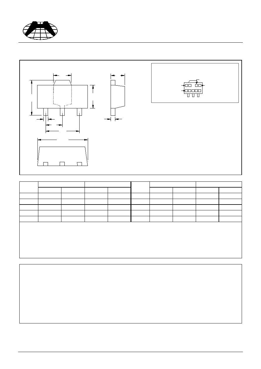
SOT-89 Dimension
*:Typical
Inches
Millimeters
Inches
Millimeters
DIM
Min.
Max.
Min.
Max.
DIM
Min.
Max.
Min.
Max.
A
0.1732
0.1811
4.40
4.60
F
0.0583
0.0598
1.48
1.52
B
0.1594
0.1673
4.05
4.25
G
0.1165
0.1197
2.96
3.04
C
0.0591
0.0663
1.50
1.70
H
0.0551
0.0630
1.40
1.60
D
0.0945
0.1024
2.40
2.60
I
0.0138
0.0161
0.35
0.41
E
0.0141
0.0201
0.36
0.51
Notes :
1.Dimension and tolerance based on our Spec. dated May. 05,1996.
2.Controlling dimension : millimeters.
3.Maximum lead thickness includes lead finish thickness, and minimum lead thickness is the minimum thickness of base material.
4.If there is any question with packing specification or packing method, please contact your local HSMC sales office.
Material :
·
Lead : 42 Alloy ; solder plating
·
Mold Compound : Epoxy resin family, flammability solid burning class:UL94V-0
Important Notice:
·
All rights are reserved. Reproduction in whole or in part is prohibited without the prior written approval of HSMC.
·
HSMC reserves the right to make changes to its products without notice.
·
HSMC semiconductor products are not warranted to be suitable for use in Life-Support Applications, or systems.
·
HSMC assumes no liability for any consequence of customer product design, infringement of patents, or application assistance.
Head Office And Factory :
·
Head Office (Hi-Sincerity Microelectronics Corp.) : 10F.,No. 61, Sec. 2, Chung-Shan N. Rd. Taipei Taiwan R.O.C.
Tel : 886-2-25212056 Fax : 886-2-25632712, 25368454
·
Factory 1 : No. 38, Kuang Fu S. Rd., Fu-Kou Hsin-Chu Industrial Park Hsin-Chu Taiwan. R.O.C
Tel : 886-3-5983621~5 Fax : 886-3-5982931
·
Factory 2 : No. 17-1, Ta-Tung Rd., Fu-Kou Hsin-Chu Industrial Park Hsin-Chu Taiwan. R.O.C
Tel : 886-3-5977061 Fax : 886-3-5979220
3
2
1
A
B
C
D
E
F
G
H
I
Style : Pin 1.Base 2.Collector 3.Emitter
Marking :
Part Number
Date Code
HSMC Logo
Package Code
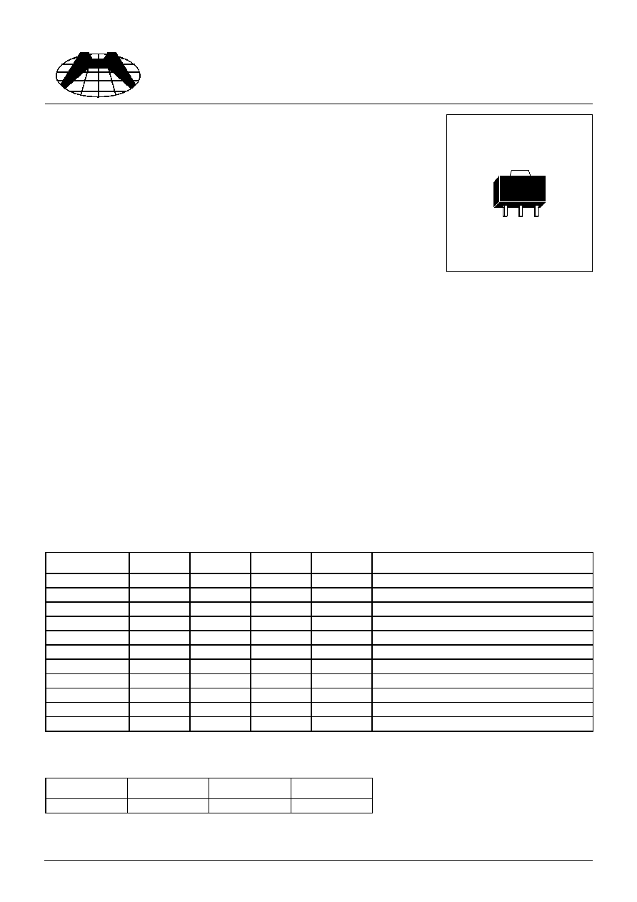
3-Lead SOT-89 Plastic Surface Mounted Package
HSMC Package Code : M