Document Outline
- þĸ
- þĸ
- þĸ
- þĸ
- þĸ
- þĸ
- þĸ
- þĸ
- þĸ
- þĸ
- þĸ
- þĸ

HT9170
DTMF Receiver
Selection Table
Function Operating
Voltage
OSC
Frequency
Tristate
Data Output
Power
Down
1633Hz
Inhibit DV DVB Package
Part No.
HT9170B 2.5V~5.5V
3.58MHz
Ö
Ö
Ö
Ö
ū
18 DIP
HT9170D 2.5V~5.5V
3.58MHz
Ö
Ö
Ö
Ö
ū
18 SOP
1
December 20, 1999
Features
·
Operating voltage: 2.5V~5.5V
·
Minimal external components
·
No external filter is required
·
Low standby current (on power down mode)
·
Excellent performance
·
Tristate data output for mC interface
·
3.58MHz crystal or ceramic resonator
·
1633Hz can be inhibited by the INH pin
·
HT9170B: 18-pin DIP package
HT9170D: 18-pin SOP package
General Description
The HT9170 series are Dual Tone Multi Fre-
quency (DTMF) receivers integrated with digi-
tal decoder and bandsplit filter functions. The
HT9170B and HT9170D types supply
power-down mode and inhibit mode operations.
All types of the HT9170 series use digital count-
ing techniques to detect and decode all the 16
DTMF tone pairs into a 4-bit code output.
Highly accurate switched capacitor filters are
employed to divide tone (DTMF) signals into
low and high group signals. A built-in dial tone
rejection circuit is provided to eliminate the
need for pre-filtering.
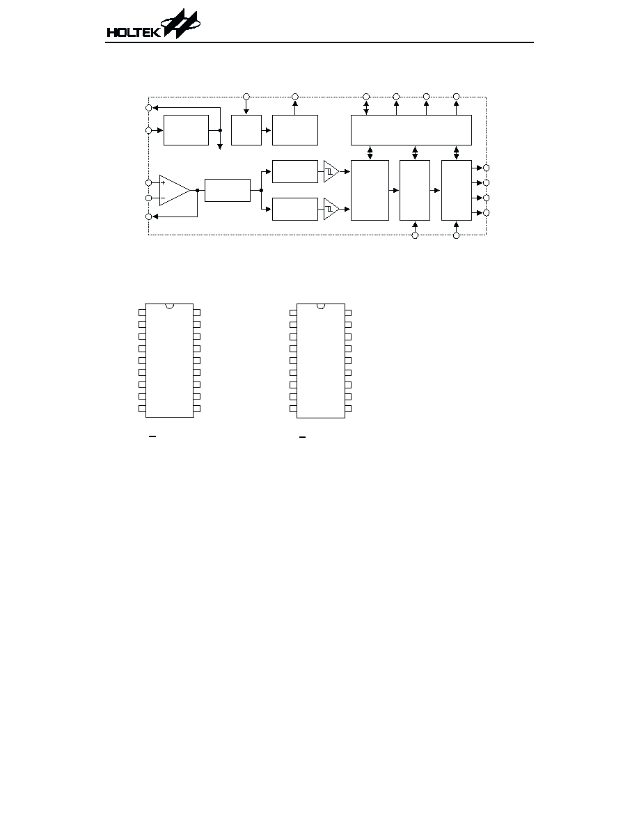
Block Diagram
Pin Assignment
HT9170
2
December 20, 1999
O P A
X 2
X 1
3 . 5 8 M H z
C r y s t a l
O s c i l l a t o r
V r e f
G e n e r a t o r
L o w G r o u p
F i l t e r
H i g h G r o u p
F i l t e r
S t e e r i n g C o n t r o l C i r c u i t
P r e - F i l t e r
V P
V N
G S
F r e q u e n c y
D e t e c t o r
C o d e
D e t e c t o r
L a t c h
&
O u t p u t
B u f f e r
O E
V R E F
R T / G T
E S T
D V
D 0
D 1
D 2
D 3
I N H
B i a s
C i r c u i t
P W D N
D V B
1 8
1 7
1 6
1 5
1 4
1 3
1 2
1 1
1 0
1
2
3
4
5
6
7
8
9
V D D
R T / G T
E S T
D V
D 3
D 2
D 1
D 0
O E
V P
V N
G S
V R E F
I N H
P W D N
X 1
X 2
V S S
1 8
1 7
1 6
1 5
1 4
1 3
1 2
1 1
1 0
1
2
3
4
5
6
7
8
9
V D D
R T / G T
E S T
D V
D 3
D 2
D 1
D 0
O E
V P
V N
G S
V R E F
I N H
P W D N
X 1
X 2
V S S
H T 9 1 7 0 B
1 8 D I P
H T 9 1 7 0 D
1 8 S O P

Pin Description
Pin Name I/O
Internal
Connection
Description
VP
I OPERATIONAL
AMPLIFIER
Operational amplifier non-inverting input
VN
I
Operational amplifier inverting input
GS
O
Operational amplifier output terminal
VREF
O
VREF
Reference voltage output, normally V
DD
/2
X1
I
OSCILLATOR
The system oscillator consists of an inverter, a bias resistor
and the necessary load capacitor on chip.
A standard 3.579545MHz crystal connected to X1 and X2 ter-
minals implements the oscillator function.
X2
O
PWDN
I
CMOS IN
Pull-low
Active high. This enables the device to go into power down
mode and inhibits the oscillator. This pin input is internally
pulled down.
INH
I
CMOS IN
Pull-low
Logic high. This inhibits the detection of tones representing
characters A, B, C and D. This pin input is internally pulled
down.
VSS
ū
ū
Negative power supply
OE
I
CMOS IN
Pull-high
D0~D3 output enable, high active
D0~D3
O
CMOS OUT
Tristate
Receiving data output terminals
OE=ēHē: Output enable
OE=ēLē: High impedance
DV
O
CMOS OUT
Data valid output
When the chip receives a valid tone (DTMF) signal, the DV
goes high; otherwise it remains low.
EST
O
CMOS OUT
Early steering output (see Functional Description)
RT/GT
I/O CMOS IN/OUT Tone acquisition time and release time can be set through
connection with external resistor and capacitor.
VDD
ū
ū
Positive power supply, 2.5V~5.5V for normal operation
DVB
O
CMOS OUT
One-shot type data valid output, normal high, when the chip
receives a valid time (DTMF) signal, the DVB goes low for
10ms.
HT9170
3
December 20, 1999
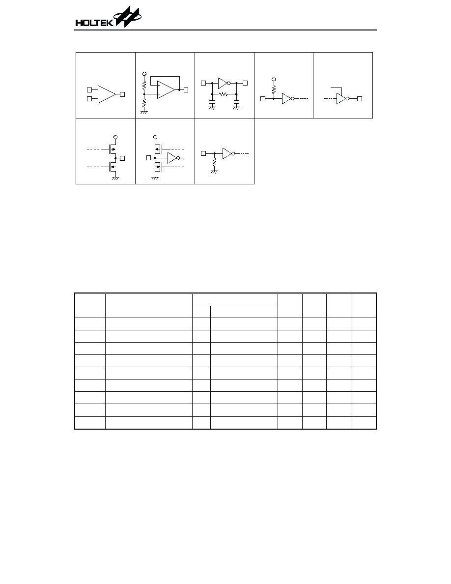
Approximate internal connection circuits
Absolute Maximum Ratings
Supply Voltage.................................-0.3V to 6V
Storage Temperature.................-50°C to 125°C
Input Voltage.................V
SS
-0.3V to V
DD
+0.3V
Operating Temperature ..............-20°C to 75°C
Note: These are stress ratings only. Stresses exceeding the range specified under ēAbsolute Maxi-
mum Ratingsē may cause substantial damage to the device. Functional operation of this device
at other conditions beyond those listed in the specification is not implied and prolonged expo-
sure to extreme conditions may affect device reliability.
D.C. Characteristics
Ta=25°C
Symbol
Parameter
Test Conditions
Min.
Typ. Max.
Unit
V
DD
Conditions
V
DD
Operating Voltage
ū
ū
2.5
5
5.5
V
I
DD
Operating Current
5V
ū
ū
3.0
7
mA
I
STB
Standby Current
5V PWDN=5V
ū
10
25
mA
V
IL
ēLowē Input Voltage
5V
ū
ū
ū
1.0
V
V
IH
ēHighē Input Voltage
5V
ū
4.0
ū
ū
V
I
IL
ēLowē Input Current
5V V
VP
=V
VN
=0V
ū
ū
0.1
mA
I
IH
ēHighē Input Current
5V V
VP
=V
VN
=5V
ū
ū
0.1
mA
R
OE
Pull-high Resistance (OE)
5V V
OE
=0V
60
100
150
kW
R
IN
Input Impedance (VN, VP) 5V
ū
ū
10
ū
MW
HT9170
4
December 20, 1999
V -
V +
O P E R A T I O N A L
A M P L I F I E R
V N
V P
G S
X 1
X 2
O S C I L L A T O R
C M O S I N
P u l l - h i g h
C M O S O U T
T r i s t a t e
E N
C M O S O U T
C M O S I N / O U T
V R E F
O P A
O P A
2 0 p F
1 0 M
1 0 p F
C M O S I N
P u l l - l o w
Symbol
Parameter
Test Conditions
Min.
Typ. Max.
Unit
V
DD
Conditions
I
OH
Source Current
(D0~D3, EST, DV)
5V V
OUT
=4.5V
-0.4
-0.8
ū
mA
I
OL
Sink Current
(D0~D3, EST, DV)
5V V
OUT
=0.5V
1.0
2.5
ū
mA
f
OSC
System Frequency
5V Crystal=3.5795MHz 3.5759 3.5795 3.5831 MHz
A.C. Characteristics
f
OSC
=3.5795MHz, Ta=25°C
Symbol
Parameter
Test Conditions
Min. Typ. Max. Unit
V
DD
Conditions
DTMF Signal
Input Signal Level
3V
-36
ū
-6
dBm
5V
-29
ū
1
Twist Accept Limit (Positive)
5V
ū
10
ū
dB
Twist Accept Limit (Negative)
5V
ū
10
ū
dB
Dial Tone Tolerance
5V
ū
18
ū
dB
Noise Tolerance
5V
ū
-12
ū
dB
Third Tone Tolerance
5V
ū
-16
ū
dB
Frequency Deviation
Acceptance
5V
ū
ū
ą1.5
%
Frequency Deviation Rejection 5V
ą3.5
ū
ū
%
Power Up Time (t
PU
)
(See Figure 4.)
5V
ū
30
ū
ms
Gain Setting Amplifier
R
IN
Input Resistance
5V
ū
ū
10
ū
MW
I
IN
Input Leakage Current
5V V
SS
<(V
VP
,V
VN
)<V
DD
ū
0.1
ū
mA
V
OS
Offset Voltage
5V
ū
ū
ą25
ū
mV
P
SRR
Power Supply Rejection
5V
100 Hz
-3V<V
IN
<3V
ū
60
ū
dB
C
MRR
Common Mode Rejection
5V
ū
60
ū
dB
A
VO
Open Loop Gain
5V
ū
65
ū
dB
f
T
Gain Band Width
5V
ū
ū
1.5
ū
MHz
V
OUT
Output Voltage Swing
5V R
L
>100kW
ū
4.5
ū
V
PP
HT9170
5
December 20, 1999