Document Outline
- Ģˇ
- Ģˇ
- Ģˇ
- Ģˇ
- Ģˇ
- Ģˇ
- Ģˇ
- Ģˇ
- Ģˇ
- Ģˇ
- Ģˇ
- Ģˇ
- Ģˇ

HT82V36
16-Bit CCD/CIS Analog Signal Processor
Block Diagram
Rev. 1.30
1
June 29, 2004
Features
∑
Operating voltage: 3.3V
∑
Low power consumption at 56mW
∑
Power-down mode: Under 1
mA
(clock timing keep low)
∑
16-bit 6 MSPS A/D converter
∑
Guaranteed no missing codes
∑
Supports CDS/SHA mode
∑
1~6 programmable gain
∑
Ī200mV programmable offset
∑
Input clamp circuitry
∑
Internal voltage reference
∑
Multiplexed byte-wide output (8+8 format)
∑
Programmable 3-wire serial interface
∑
3.3V digital I/O compatibility
∑
28-pin SSOP (209mil) package
C D S
+
M U X
G I N
P G A
C L A M P
9 B i t s
D A C
1 6 B i t s
A / D
C o n v e r t e r
R E G I S T E R S
B A N D G A P
9
6
1 6
D 0 ~ D 7
S L O A D
S D A T A
S C L K
General Description
The HT82V36 is a complete analog signal processor for
CCD imaging applications. It features a 1-channel archi-
tecture designed to sample and condition the outputs of
linear CCD arrays. It consists of an input clamp, Corre-
lated Double Sampler (CDS), offset DAC and Program-
mable Gain Amplifier (PGA), and a low power 16-bit A/D
converter.
The CDS amplifiers may be disabled for use with sen-
sors such as Contact Image Sensors (CIS) and CMOS
active pixel sensors, which do not require CDS.
The 16-bit digital output is multiplexed into an 8-bit out-
put word that is accessed using two read cycles. The in-
ternal registers are programmed through a 3-wire serial
interface, which provides gain, offset and operating
mode adjustments.
Applications
Low power flatbed document scanners
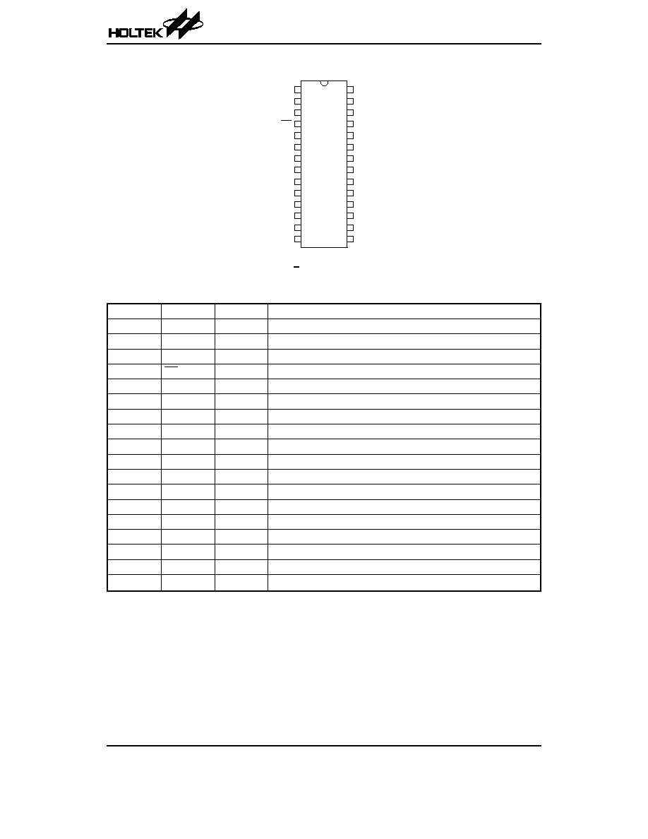
Pin Assignment
Pin Description
Pin No.
Pin Name
I/O
Description
1
CDSCLK1
DI
CDS reference clock pulse input
2
CDSCLK2
DI
CDS data clock pulse input
3
ADCCLK
DI
A/D sample clock input
4
OE
DI
Output enable, active low
5
DRVDD
P
Digital driver power
6
DRVSS
P
Digital driver ground
7~14
D7~D0
DO
Digital data output
15
SDATA
DI/DO
Serial data input/output
16
SCLK
DI
Clock input for serial interface
17
SLOAD
DI
Serial interface load pulse
18, 27
AVSS
P
Analog ground
19, 28
AVDD
P
Analog supply
20
REFB
AO
Reference decoupling
21
REFT
AO
Reference decoupling
23
CML
AO
Internal reference output
24
VING
AI
Analog input
25
OFFSET
AO
Clamp bias level decoupling
22, 26
NC
ĺ
No connection
Absolute Maximum Ratings
Supply Voltage ..........................V
SS
-0.3V to V
SS
+3.6V
Storage Temperature ...........................
-50įC to 125įC
Input Voltage .............................V
SS
-0.3V to V
DD
+0.3V
Operating Temperature ..........................
-25įC to 75įC
Note: These are stress ratings only. Stresses exceeding the range specified under
≤Absolute Maximum Ratings≤ may
cause substantial damage to the device. Functional operation of this device at other conditions beyond those
listed in the specification is not implied and prolonged exposure to extreme conditions may affect device reliabil-
ity.
HT82V36
Rev. 1.30
2
June 29, 2004
2 8
2 7
2 6
2 5
2 4
2 3
2 2
2 1
2 0
1 9
1 8
1 7
1 6
1 5
1
2
3
4
5
6
7
8
9
1 0
1 1
1 2
1 3
1 4
A V D D
A V S S
N C
O F F S E T
V I N G
C M L
N C
R E F T
R E F B
A V S S
A V D D
S L O A D
S C L K
S D A T A
C D S C L K 1
C D S C L K 2
A D C C L K
O E
D R V D D
D R V S S
D 7 ( M S B )
D 6
D 5
D 4
D 3
D 2
D 1
D 0 ( L S B )
H T 8 2 V 3 6
2 8 S S O P - A

D.C. Characteristics
Symbol
Parameter
Test Conditions
Min.
Typ.
Max.
Unit
V
DD
Conditions
Logic Inputs
V
IH
High Level Input Voltage
ĺ
ĺ
0.8
īV
DD
ĺ
ĺ
V
V
IL
Low Level Input Voltage
ĺ
ĺ
ĺ
ĺ
0.2
īV
DD
V
I
IH
High Level Input Current
ĺ
ĺ
ĺ
10
ĺ
mA
I
IL
Low Level Input Current
ĺ
ĺ
ĺ
10
ĺ
mA
C
IN
Input Capacitance
ĺ
ĺ
ĺ
10
ĺ
pF
Logic Outputs
V
OH
High Level Output Voltage
ĺ
ĺ
V
DD
-0.5
ĺ
ĺ
V
V
OL
Low Level Output Voltage
ĺ
ĺ
ĺ
ĺ
0.5
V
I
OH
High Level Output Voltage
ĺ
ĺ
ĺ
1
ĺ
mA
I
OL
Low Level Output Voltage
ĺ
ĺ
ĺ
1
ĺ
mA
A.C. Characteristics
Symbol
Parameter
Test Conditions
Min.
Typ.
Max.
Unit
V
DD
Conditions
Maximum Conversion Rate
t
MAX
CDS/SHA Mode
ĺ
ĺ
6
ĺ
ĺ
MHz
Accuracy (Entire Signal Path)
ADC Resolution
ĺ
ĺ
ĺ
16
ĺ
Integral Nonlinear (INL)
ĺ
ĺ
ĺ
Ī16
ĺ
LSB
Differential Nonlinear (DNL)
ĺ
ĺ
-1
ĺ
2
LSB
Offset Error
ĺ
ĺ
-100
TBD
100
mV
Gain Error
ĺ
ĺ
ĺ
TBD
ĺ
%FSR
Analog Inputs
R
FS
Full-scale Input Range
ĺ
ĺ
1.3
1.4
1.6
Vp-p
V
i
Input Limits
ĺ
ĺ
AVDD-0.3
ĺ
AVDD+0.3
V
C
i
Input Capacitance
ĺ
ĺ
ĺ
TBD
ĺ
pF
I
i
Input Current
ĺ
ĺ
ĺ
TBD
ĺ
mA
Amplifiers
PGA Gain at Minimum
ĺ
ĺ
ĺ
1
ĺ
V/V
PGA Gain at Maximum
ĺ
ĺ
ĺ
5.85
ĺ
V/V
PGA Gain Resolution
ĺ
ĺ
ĺ
6
ĺ
Bits
Programmable Offset at Minimum
ĺ
ĺ
ĺ
-200
ĺ
mV
Programmable Offset at Maximum
ĺ
ĺ
ĺ
200
ĺ
mV
Offset Resolution
ĺ
ĺ
ĺ
9
ĺ
Bits
Temperature Range
t
A
Operating
ĺ
ĺ
0
ĺ
70
įC
Power Supplies
V
ADD
AVDD
ĺ
ĺ
3
3.3
3.6
V
V
DRDD
DRVDD
ĺ
ĺ
3
3.3
3.6
V
Power Consumption
P
tot
Total Power Consumption
ĺ
ĺ
ĺ
56
ĺ
mW
HT82V36
Rev. 1.30
3
June 29, 2004

Timing Specification
Symbol
Parameter
Min.
Typ.
Max.
Unit
Clock Parameters
t
ADCLK
Pixel Rate Clock
166
ĺ
ĺ
ns
t
ADH
ADCCLK Pulse High Width
80
ĺ
ns
t
ADL
ADCCLK Pulse Low Width
80
ĺ
ns
t
C1
CDSCLK1 Pulse Width
20
ĺ
ĺ
ns
t
C2
CDS Mode CDSCLK2 Pulse Width
20
ĺ
ĺ
ns
t
C3
SHA Mode CDSCLK2 Pulse Width
40
ĺ
ĺ
ns
t
C2ADF
CDSCLK2 Falling to ADCCLK Falling
60
ĺ
ĺ
ns
t
ADFC1
ADCCLK Falling to CDSCLK1 Rising
2
ĺ
ĺ
ns
t
ADFC2
ADCCLK Falling to CDSCLK2 Rising
2
ĺ
ĺ
ns
t
AD
Analog Sampling Delay
5
ĺ
ĺ
ns
Serial Interface
f
SCLK
Maximum SCLK Frequency
10
ĺ
ĺ
MHz
t
LS
SLOAD to SCLK Setup Time
10
ĺ
ĺ
ns
t
LH
SCLK to SLOAD Hold Time
10
ĺ
ĺ
ns
t
DS
SDATA to SCLK Rising Setup Time
10
ĺ
ĺ
ns
t
DH
SCLK Rising to SDATA Hold Time
10
ĺ
ĺ
ns
t
RDV
Falling to SDATA Valid
10
ĺ
ĺ
ns
Data Output
t
OD
Output Delay
ĺ
8
ĺ
ns
Latency (Pipeline Delay)
ĺ
9
ĺ
Cycles
HT82V36
Rev. 1.30
4
June 29, 2004
Functional Description
Integral Nonlinear (INL)
Integral nonlinear error refers to the deviation of each in-
dividual code from a line drawn from zero scale through
positive full scale. The point used as zero scale occurs 1
/2 LSB before the first code transition. Positive full scale
is defined as a level 1/2 LSB beyond the last code transi-
tion. The deviation is measured from the middle of each
particular code to the true straight line.
Differential Nonlinear (DNL)
An ideal ADC exhibits code transitions that are exactly 1
LSB apart. DNL is the deviation from this ideal value.
Thus every code must have a finite width. No missing
codes guaranteed to 16-bit resolution indicates that all
4096 codes, respectively, must be present over all oper-
ating ranges.
Offset Error
The first ADC code transition should occur at a level 1/2
LSB above the nominal zero scale voltage.
The offset error is the deviation of the actual first code
transition level from the ideal level.
Gain Error
The last code transition should occur for an analog
value 1/2 LSB below the nominal full-scale voltage.
Gain error is the deviation of the actual difference be-
tween first and last code transitions and the ideal differ-
ence between the first and last code transitions.
Aperture Delay
The aperture delay is the time delay that occurs when a
sampling edge is applied to the HT82V36 until the actual
sample of the input signal is held. Both CDSCLK1 and
CDSCLK2 sample the input signal during the transition
from high to low, so the aperture delay is measured from
each clock
Ęs falling edge to the instant the actual inter-
nal sample is taken.

HT82V36
Rev. 1.30
5
June 29, 2004
Internal Register Descriptions
Register
Name
Address
Data Bits
A2
A1
A0
D8
D7
D6
D5
D4
D3
D2
D1
D0
Configuration
0
0
0
0
0
1
1
CDS on
Clamp
Voltage
Enable
Power
Down
Output
Delay
1byte
out
Reserved
0
0
1
Reserved
0
1
0
PGA
0
1
1
X
0
0
MSB
LSB
Reserved
1
0
0
Reserved
1
0
1
Offset
1
1
0
MSB
LSB
Reserved
1
1
1
Internal Register Map
D8
D7
D6
D5
D4
D3
D2
D1
D0
Set to 0 Set to 0 Set to 1 Set to 1
CDS operation Clamp bias Power-down
Output delay
1 byte out
(High-byte only)
1=CDS mode*
1=2.5V*
1=On
1=On
1=On
0=SHA mode
0=2V
0=Off (Normal)* 0=Off*
0=Off*
Configuration Register Settings
Note: * Power-on default value
PGA Gain Register
Bits D7 and D6 in the register must be set low, and bits D5 through D0 control the gain range in 64 increments. See fig-
ure for a graph of the PGA gain versus PGA register code. The coding for the PGA register is straight binary, with an all
zero words corresponding to the minimum gain setting (1x) and an all one word corresponding to the maximum gain
setting (5.85x).
The PGA has a gain range from 1x (0dB) to 5.85x (15.3dB), adjustable in 64 steps. The Figure shows the PGA gain as a
function of the PGA register code. Although the gain curve is approximately linear in dB, the gain in V/V varies in non-
linear proportion with the register code, according to the following the equation: Gain=
5.85
1
4.85
(
63
G
63
)
+
ī
-
Where G is the decimal value of the gain register contents, and varies from 0 to 63.
PGA Gain Transfer Function
1 2 1 6 2 0 2 4 2 8 3 2 3 6 4 0 4 4 4 8 5 2 5 6 6 0
0
4
8
6 3
1 5
1 2
9
6
3
0
5 . 8 5
5 . 0
4 . 0
3 . 0
2 . 0
1 . 0
G
A
I
N
-
d
B
(
)
G
A
I
N
-
V
/
V
(
)
P G A r e g i s t e r v a l u e - - D e c i m a l
ī