Äîêóìåíòàöèÿ è îïèñàíèÿ www.docs.chipfind.ru

HT82M99EE/HT82M99AE
USB Mouse Encoder 8-Bit MCU
Rev. 1.00
1
February 8, 2006
General Description
The USB MCU HT82M99EE/HT82M99AE are suitable
for USB mouse and USB joystick devices. It consists of
a Holtek high performance 8-bit MCU core for control
unit, built-in USB SIE, 2K
´14 program memory and 96
bytes data RAM.
The mask version HT82M99AE is fully pin and function-
ally compatible with the OTP version HT82M99EE de-
vice.
There are two dice in the HT82M99EE/HT82M99AE
package: one is the HT82M99EE/HT82M99AE MCU,
the other is a 128
´8 bits EEPROM used for data mem-
ory purpose. The two dice are wire-bonded to form
HT82M99EE/HT82M99AE.
Features
·
Flexible total solution for applications that combine
PS/2 and low-speed USB interface, such as mice,
joysticks, and many others
·
USB Specification Compliance
-
Conforms to USB specification V1.1
-
Conforms to USB HID specification V1.1
·
Supports 1 Low-speed USB control endpoint and 1
interrupt endpoint
·
Each endpoint has 8
´8 bytes FIFO
·
Integrated USB transceiver
·
3.3V regulator output
·
External 6MHz or 12MHz ceramic resonator or crys-
tal
·
8-bit RISC microcontroller, with 2K
´14 program
memory (000H~7FFH)
·
96 bytes RAM (20H~7FH)
·
128
´8 data EEPROM
·
6MHz/12MHz internal CPU clock
·
4-level stacks
·
Two 7-bit indirect addressing registers
·
One 16-bit programmable timer counter with over-
flow interrupt (shared with PA7, vector 0CH)
·
One USB interrupt input (vector 04H)
·
HALT function and wake-up feature reduce power
consumption
·
PA0~PA7, PB4 and PB7 support wake-up function
·
Internal Power-On reset (POR)
·
Watchdog Timer (WDT)
·
12 I/O ports
·
20-pin DIP/SOP package
Technical Document
·
Tools Information
·
FAQs
·
Application Note
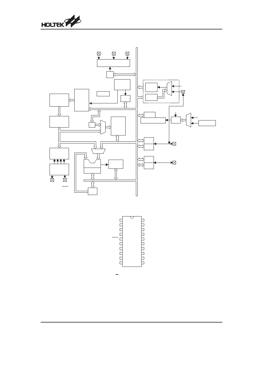
Block Diagram
Pin Assignment
HT82M99EE/HT82M99AE
Rev. 1.00
2
February 8, 2006
O S C 2
O S C 1
R E S
V D D
M U X
T M R C
T M R L
T M R H
V S S
P r o g r a m
R O M
P r o g r a m
C o u n t e r
I n t e r r u p t
C i r c u i t
S T A C K
I N T C
D a t a
M e m o r y
I n s t r u c t i o n
R e g i s t e r
M
U
X
I n s t r u c t i o n
D e c o d e r
S T A T U S
A L U
S h i f t e r
T i m i n g
G e n e r a t o r
A C C
M
U
X
M P
S Y S C L K / 4
W D T S
W D T
W D T O S C
W D T P r e s c a l e r
M
U
X
E N / D I S
P B C
P O R T B
P B
P A C
P O R T A
P A
f
S Y S
/ 4
P A 7 / T M R
U S B 1 . 1
P S 2
B P
U S B D + / C L K U S B D - / D A T A V 3 3 O
P A 0 ~ P A 6
P A 7 / T M R
P B 2 ~ P B 3
P B 4 / S D A
P B 7 / S C L
2 0
1 9
1 8
1 7
1 6
1 5
1 4
1 3
1 2
1 1
1
2
3
4
5
6
7
8
9
1 0
H T 8 2 M 9 9 E E / H T 8 2 M 9 9 A E
2 0 D I P - A / S O P - A
V S S
V 3 3 O
U S B D + / C L K
U S B D - / D A T A
R E S
P A 0
P A 1
P B 2
P B 3
P B 4 / S D A
O S C I
O S C O
V D D
P A 7 / T M R
P A 6
P A 5
P A 4
P A 3
P A 2
P B 7 / S C L
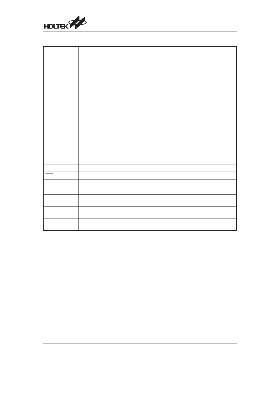
Pin Description
Pin Name
I/O
ROM Code
Option
Description
PA0~PA6
PA7/TMR
I/O
Pull-low
Pull-high
Wake-up
CMOS/NMOS/PMOS
Bidirectional 8-bit input/output port. Each bit can be configured as a
wake-up input by ROM code option. The input or output mode is con-
trolled by PAC (PA control register).
Pull-high resistor options: PA0~PA7
Pull-low resistor options: PA0~PA3
CMOS/NMOS/PMOS options: PA0~PA7
Falling edge wake-up options: PA0~PA1, PA4~PA7
Rising and falling edge wake-up options: PA2~PA3
PA7 is wire-bonded with TMR
PB2~PB3
I/O
Pull-high
Pull-low
Bidirectional 8-bit input/output port. Software instructions determine the
CMOS output or Schmitt trigger input with pull-high resistor (determined
by pull-high options).
Pull-low resistor for options: PB2, PB3
PB4/SDA,
PB7/SCL
I/O
Pull-high
Wake-up
Bidirectional 8-bit input/output port. Software instructions determine the
CMOS output or Schmitt trigger input with pull-high resistor (determined
by pull-high options).
The PB can be used as analog input of the analog to digital converter
(determined by options).
Falling edge wake-up options: PB4, PB7
PB4 is wire-bonded with SDA pad of the Data EEPROM
PB7 is wire-bonded with SCL pad of the Data EEPROM
VSS
¾
¾
Negative power supply, ground
RES
I
¾
Schmitt trigger reset input. Active low.
VDD
¾
¾
Positive power supply
V33O
O
¾
3.3V regulator output
USBD+/CLK
I/O
¾
USBD+ or PS2 CLK I/O line
USB or PS2 function is controlled by software control register
USBD-/DATA
I/O
¾
USBD- or PS2 DATA I/O line
USB or PS2 function is controlled by software control register
OSCI
OSCO
I
O
¾
OSCI, OSCO are connected to a 6MHz or 12MHz crystal/resonator (de-
termined by software instructions) for the internal system clock.
Absolute Maximum Ratings
Supply Voltage ...........................V
SS
-0.3V to V
SS
+6.0V
Storage Temperature ............................
-50°C to 125°C
Input Voltage..............................V
SS
-0.3V to V
DD
+0.3V
Operating Temperature...............................0
°C to 70°C
Note: These are stress ratings only. Stresses exceeding the range specified under
²Absolute Maximum Ratings² may
cause substantial damage to the device. Functional operation of this device at other conditions beyond those
listed in the specification is not implied and prolonged exposure to extreme conditions may affect device reliabil-
ity.
HT82M99EE/HT82M99AE
Rev. 1.00
3
February 8, 2006
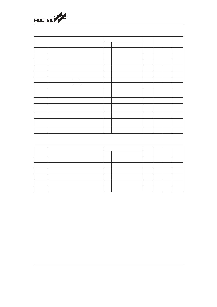
D.C. Characteristics
Ta=25
°C
Symbol
Parameter
Test Conditions
Min.
Typ.
Max.
Unit
V
DD
Conditions
V
DD
Operating Voltage
¾
¾
4
¾
5.5
V
I
DD
Operating Current (6MHz Crystal)
5V
No load, f
SYS
=6MHz
¾
7
9
mA
I
STB
Standby Current
5V
No load, system HALT
¾
300
500
mA
V
IL1
Input Low Voltage for I/O Ports
5V
¾
0
¾
0.8
V
V
IH1
Input High Voltage for I/O Ports
5V
¾
2
¾
5
V
V
IL2
Input Low Voltage (RES)
5V
¾
0
¾
0.4V
DD
V
V
IH2
Input High Voltage (RES)
5V
¾
0.9V
DD
¾
V
DD
V
I
OL
Output Sink Current for Other Ports
PA0~PA7, PB2~PB4, PB7
5V
V
OL
=0.4V
2
4
¾
mA
I
OH
Output Port Source Current
5V
V
OL
=3.4V
-2.5
-4
¾
mA
R
PD
Pull-down Resistance for PA0~PA3, PB2
and PB3
5V
¾
10
30
50
k
W
R
PH1
Pull-high Resistance for CLK and DATA
¾
¾
2
4.7
6
k
W
R
PH2
Pull-high Resistance for PA0~PA7,
PB2~PB4, PB7
¾
¾
30
50
70
k
W
V
LVR
Low Voltage Reset
5V
¾
2.4
2.7
3
V
A.C. Characteristics
Ta=25
°C
Symbol
Parameter
Test Conditions
Min.
Typ.
Max.
Unit
V
DD
Conditions
f
SYS
System Clock (Crystal OSC)
5V
¾
6
¾
12
MHz
f
RCSYS
RC Clock with 8-bit Prescaler Register
5V
¾
0
32
¾
kHz
t
WDT
Watchdog Time-out Period (System Clock)
¾ Without WDT prescaler 1024
¾
¾
t
RCSYS
t
RF
USBD+, USBD- Rising & falling Time
¾
¾
75
¾
300
ns
t
SST
System Start-up Timer Period
¾ Wake-up from HALT
¾
1024
¾
t
SYS
t
OSC
Crystal Setup
¾
¾
¾
5
10
ms
Note: Power-on period=t
WDT
+t
SST
+t
OSC
WDT Time-out in normal mode=1/f
RCSYS
´256´WDTS+t
WDT
WDT Time-out in HALT mode=1/f
RCSYS
´256´WDTS+t
SST
+t
OSC
HT82M99EE/HT82M99AE
Rev. 1.00
4
February 8, 2006
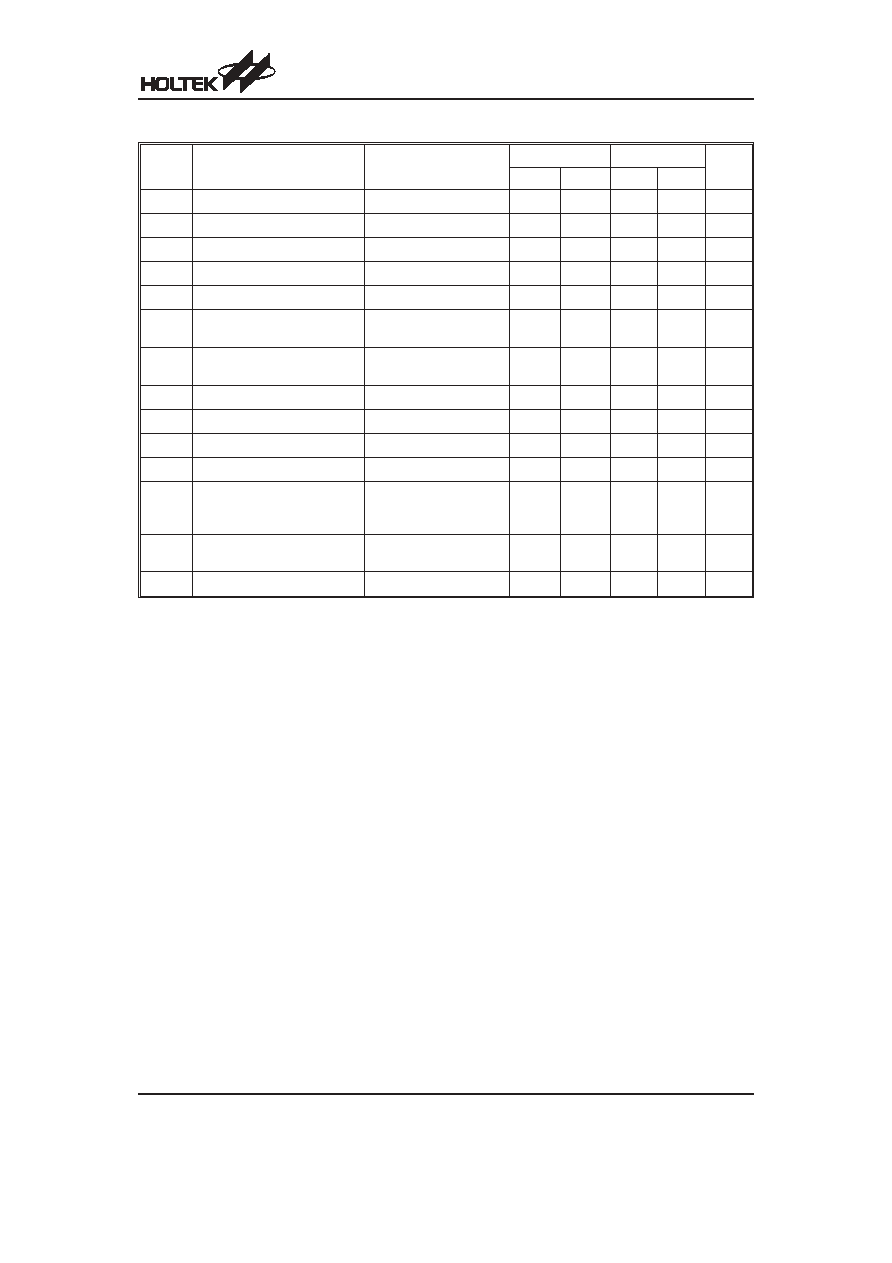
EEPROM A.C. Characteristics
Ta=25
°C
Symbol
Parameter
Remark
Standard Mode*
V
CC
=5V
±10%
Unit
Min.
Max.
Min.
Max.
f
SK
Clock Frequency
¾
¾
100
¾
400
kHz
t
HIGH
Clock High Time
¾
4000
¾
600
¾
ns
t
LOW
Clock Low Time
¾
4700
¾
1200
¾
ns
t
r
SDA and SCL Rise Time
Note
¾
1000
¾
300
ns
t
f
SDA and SCL Fall Time
Note
¾
300
¾
300
ns
t
HD:STA
START Condition Hold Time
After this period the first
clock pulse is generated
4000
¾
600
¾
ns
t
SU:STA
START Condition Setup Time
Only relevant for repeated
START condition
4000
¾
600
¾
ns
t
HD:DAT
Data Input Hold Time
¾
0
¾
0
¾
ns
t
SU:DAT
Data Input Setup Time
¾
200
¾
100
¾
ns
t
SU:STO
STOP Condition Setup Time
¾
4000
¾
600
¾
ns
t
AA
Output Valid from Clock
¾
¾
3500
¾
900
ns
t
BUF
Bus Free Time
Time in which the bus must
be free before a new trans-
mission can start
4700
¾
1200
¾
ns
t
SP
Input Filter Time Constant
(SDA and SCL Pins)
Noise suppression time
¾
100
¾
50
ns
t
WR
Write Cycle Time
¾
¾
5
¾
5
ms
Note: These parameters are periodically sampled but not 100% tested
* The standard mode means V
CC
=2.2V to 5.5V
For relative timing, refer to timing diagrams
HT82M99EE/HT82M99AE
Rev. 1.00
5
February 8, 2006
Document Outline
- þÿ
- þÿ
- þÿ
- þÿ
- þÿ
- þÿ
- Absolute Maximum Ratings
- þÿ
- þÿ
- þÿ
- þÿ
- þÿ
- þÿ
- þÿ
- þÿ
- þÿ
- þÿ